


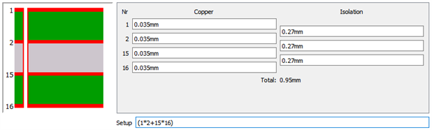
Hi, I'm trying to create a 4 layer PCB (TOP + POWER + GND + BOTTOM). I created 2 planes for the VBB and GNDBB using polygons.
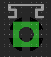
My problem is the connection (let's say) beetween a resistor and the PAD of a component (let's call it X component). If try to connect the VBB connection of the resistor to a Via (and the via's name is VBB) the VBB PAD of the X component with appear like the pic below and the airwire that was connecting the resistor to the X component is gone!
But if I try to do the same with a resistor that is connected to a GND pad, the pad stays the same and the airwire is still there, which makes me wonder if the vias are even connecting to the GND plan.
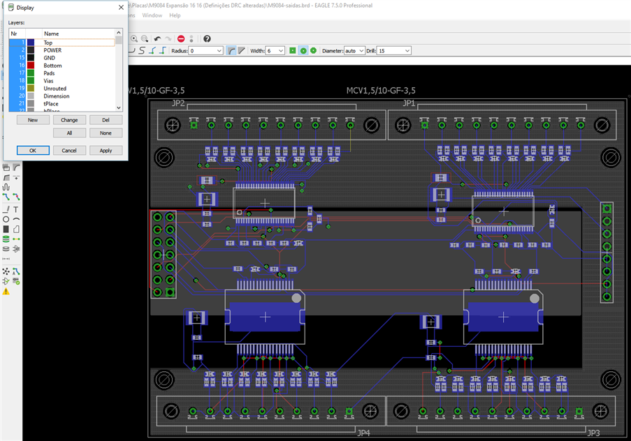
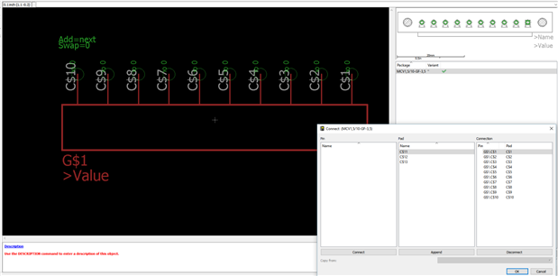
The following are printscreens of the settings I'm currently using.
What am I doing wrong here?
Any help would be highly appreciated!

