element14 Community
element14 Community
    Register Log In
  • Site
  • Search
  • Log In Register
  • Community Hub
    Community Hub
    • What's New on element14
    • Feedback and Support
    • Benefits of Membership
    • Personal Blogs
    • Members Area
    • Achievement Levels
  • Learn
    Learn
    • Ask an Expert
    • eBooks
    • element14 presents
    • Learning Center
    • Tech Spotlight
    • STEM Academy
    • Webinars, Training and Events
    • Learning Groups
  • Technologies
    Technologies
    • 3D Printing
    • FPGA
    • Industrial Automation
    • Internet of Things
    • Power & Energy
    • Sensors
    • Technology Groups
  • Challenges & Projects
    Challenges & Projects
    • Design Challenges
    • element14 presents Projects
    • Project14
    • Arduino Projects
    • Raspberry Pi Projects
    • Project Groups
  • Products
    Products
    • Arduino
    • Avnet & Tria Boards Community
    • Dev Tools
    • Manufacturers
    • Multicomp Pro
    • Product Groups
    • Raspberry Pi
    • RoadTests & Reviews
  • About Us
  • Store
    Store
    • Visit Your Store
    • Choose another store...
      • Europe
      •  Austria (German)
      •  Belgium (Dutch, French)
      •  Bulgaria (Bulgarian)
      •  Czech Republic (Czech)
      •  Denmark (Danish)
      •  Estonia (Estonian)
      •  Finland (Finnish)
      •  France (French)
      •  Germany (German)
      •  Hungary (Hungarian)
      •  Ireland
      •  Israel
      •  Italy (Italian)
      •  Latvia (Latvian)
      •  
      •  Lithuania (Lithuanian)
      •  Netherlands (Dutch)
      •  Norway (Norwegian)
      •  Poland (Polish)
      •  Portugal (Portuguese)
      •  Romania (Romanian)
      •  Russia (Russian)
      •  Slovakia (Slovak)
      •  Slovenia (Slovenian)
      •  Spain (Spanish)
      •  Sweden (Swedish)
      •  Switzerland(German, French)
      •  Turkey (Turkish)
      •  United Kingdom
      • Asia Pacific
      •  Australia
      •  China
      •  Hong Kong
      •  India
      •  Korea (Korean)
      •  Malaysia
      •  New Zealand
      •  Philippines
      •  Singapore
      •  Taiwan
      •  Thailand (Thai)
      • Americas
      •  Brazil (Portuguese)
      •  Canada
      •  Mexico (Spanish)
      •  United States
      Can't find the country/region you're looking for? Visit our export site or find a local distributor.
  • Translate
  • Profile
  • Settings
Autodesk EAGLE
  • Products
  • More
Autodesk EAGLE
EAGLE User Support (English) Unable to see the copper pour on the PAD though the thermels is off
  • Blog
  • Forum
  • Documents
  • Events
  • Polls
  • Files
  • Members
  • Mentions
  • Sub-Groups
  • Tags
  • More
  • Cancel
  • New
Join Autodesk EAGLE to participate - click to join for free!
Actions
  • Share
  • More
  • Cancel
Forum Thread Details
  • State Verified Answer
  • Replies 6 replies
  • Answers 2 answers
  • Subscribers 180 subscribers
  • Views 1567 views
  • Users 0 members are here
  • eagle cad
  • eagle help
Related

Unable to see the copper pour on the PAD though the thermels is off

siddharthtaunk
siddharthtaunk over 8 years ago

Hi,


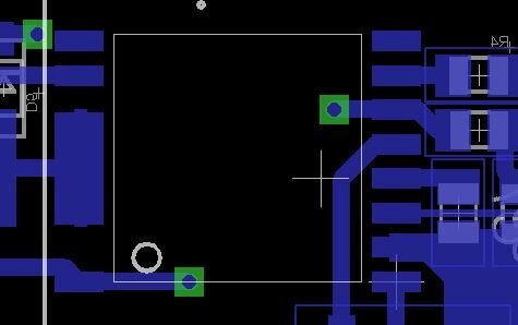
I am designing a power supply PCB I have a polygon covering the PAD of one of the ICs There are several small PADS and a big PAD. Now when polygon on the top of the small pads and have the thermals off I see that the polygon fills only the small PADS completely but there is a problem with the large PAD.


How do I resolve this.

Here is the picture for the same


Thanks and regards.

Siddharth

image

  • Sign in to reply
  • Cancel

Top Replies

  • autodeskguest
    autodeskguest over 8 years ago in reply to siddharthtaunk +2 verified
    On 18/06/17 12:19, Siddharth Taunk wrote: I have one more thing to add. When I have that perticulaer component on the TOP SIDE why is that it is effecting the PCB on the BOTTOM You answered that in you…
  • niteowl12
    niteowl12 over 8 years ago +1 suggested
    Look at the Isolate setting on the polygon. I have had it set so high that it wont even make a connection to a pin. I would also check the layout of the pad itself. There is a check box for thermals there…
  • siddharthtaunk
    siddharthtaunk over 8 years ago in reply to niteowl12 +1
    Hi, Thanks for the response. I got the reason behind those polygons not filling the complete area near the PADS. the reason being the "Dimensions". Due to that dimensions lines It is only allowing the…
Parents
  • niteowl12
    0 niteowl12 over 8 years ago

    Look at the Isolate setting on the polygon. I have had it set so high that it wont even make a connection to a pin.


    I would also check the layout of the pad itself. There is a check box for thermals there too.


    -Jason

    • Cancel
    • Vote Up +1 Vote Down
    • Sign in to reply
    • Verify Answer
    • Reject Answer
    • Cancel
Reply
  • niteowl12
    0 niteowl12 over 8 years ago

    Look at the Isolate setting on the polygon. I have had it set so high that it wont even make a connection to a pin.


    I would also check the layout of the pad itself. There is a check box for thermals there too.


    -Jason

    • Cancel
    • Vote Up +1 Vote Down
    • Sign in to reply
    • Verify Answer
    • Reject Answer
    • Cancel
Children
  • siddharthtaunk
    0 siddharthtaunk over 8 years ago in reply to niteowl12

    Hi,


    Thanks for the response.

    I got the reason behind those polygons not filling the complete area near the PADS. the reason being the "Dimensions". Due to that dimensions lines It is only allowing the trace not the polygons to fill. How do I overcome from this?


    Thanks and regards.

    Siddharth

    • Cancel
    • Vote Up +1 Vote Down
    • Sign in to reply
    • Verify Answer
    • Cancel
  • siddharthtaunk
    0 siddharthtaunk over 8 years ago in reply to niteowl12

    I have one more thing to add.


    When I have that perticulaer component on the TOP SIDE why is that it is effecting the PCB on the BOTTOM

    • Cancel
    • Vote Up 0 Vote Down
    • Sign in to reply
    • Verify Answer
    • Cancel
  • autodeskguest
    0 autodeskguest over 8 years ago in reply to siddharthtaunk

    On 18/06/17 12:19, Siddharth Taunk wrote:

    I have one more thing to add.


    When I have that perticulaer component on the TOP SIDE why is that it is effecting the PCB on the BOTTOM


    You answered that in you previous post. The problem you have is with

    objects in the DIMENSION layer. This layer represents edges of the

    board, which clearly affects ALL layers.


    Why have you got anything in the dimension layer in your component?


    • Cancel
    • Vote Up +2 Vote Down
    • Sign in to reply
    • Verify Answer
    • Reject Answer
    • Cancel
  • siddharthtaunk
    0 siddharthtaunk over 8 years ago in reply to autodeskguest

    Hi,


    Thank you, My bad, I designed the component thinking about the dimension of the particular component, Should I change it to tPlace?

    Siddharth

    • Cancel
    • Vote Up +1 Vote Down
    • Sign in to reply
    • Verify Answer
    • Cancel
  • autodeskguest
    0 autodeskguest over 8 years ago in reply to siddharthtaunk

    On 18/06/17 12:37, Siddharth Taunk wrote:

    Hi,


    Thank you, My bad, I designed the component thinking about the dimension of the particular component, Should I change it to tPlace?

    Siddharth


    tPlace is probably the layer you intended, yes. It's used for the

    silkscreen. There's also tDocu for additional outline segments that you

    don't want on the silkscreen (e.g. because they overlap pads)


    • Cancel
    • Vote Up 0 Vote Down
    • Sign in to reply
    • Verify Answer
    • Reject Answer
    • Cancel
element14 Community

element14 is the first online community specifically for engineers. Connect with your peers and get expert answers to your questions.

  • Members
  • Learn
  • Technologies
  • Challenges & Projects
  • Products
  • Store
  • About Us
  • Feedback & Support
  • FAQs
  • Terms of Use
  • Privacy Policy
  • Legal and Copyright Notices
  • Sitemap
  • Cookies

An Avnet Company © 2025 Premier Farnell Limited. All Rights Reserved.

Premier Farnell Ltd, registered in England and Wales (no 00876412), registered office: Farnell House, Forge Lane, Leeds LS12 2NE.

ICP 备案号 10220084.

Follow element14

  • X
  • Facebook
  • linkedin
  • YouTube