


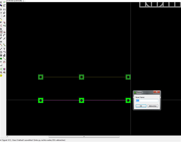
I have a .brd file with 100 pairs of through-hole vias (see the green vias in attached image). Each pair is supposed to be used as power and ground for micro-devices.
The via's outer diameter is .5 mm and the actual via hole is .15 mm. Since it is quite difficult to solder to such small vias to wires, I was thinking about routing traces from vias to pads for pin headers at the edge of the board.
The problem is since this is a .brd file (no schematic) and there is no other components except vias I cannot use the autoroute function. Is there a way to auto-route the traces from vias to pads for external header connectors?


