Hi all,
I am trying to create a custom pad shape in Eagle 6.0. I have read many 'tutorials' on how to do so but I am still having problems. Hopefully someone here can point out where I am going wrong.
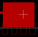
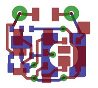
I start by making the shape I need using the polygon tool, then I insert an SMD pad into the polygon so that I have somewhere to route to (I just place a SMD pad after the polygon, no clever attachment).
At first this method seemed to work, but recently I have noticed that the autorouter sometimes routes tracks through the polygon as if it isn't there (creating a short). The polygon is on layer 1 as is the SMD pad.
Is there a way of making the entire polygon the pad?
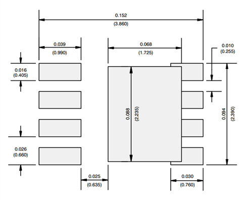
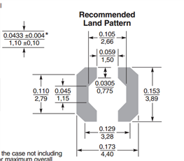
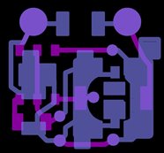
.jpg's attached for clarification.
Thanks in advance for any help.
Attachments:
 | |
 |