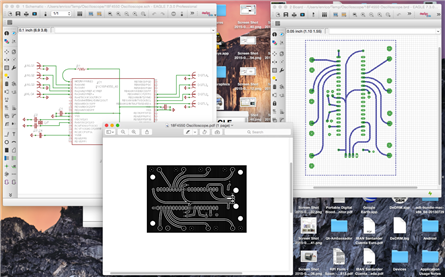
element14 Community
element14 Community
    Register Log In
  • Site
  • Search
  • Log In Register
  • Community Hub
    Community Hub
    • What's New on element14
    • Feedback and Support
    • Benefits of Membership
    • Personal Blogs
    • Members Area
    • Achievement Levels
  • Learn
    Learn
    • Ask an Expert
    • eBooks
    • element14 presents
    • Learning Center
    • Tech Spotlight
    • STEM Academy
    • Webinars, Training and Events
    • Learning Groups
  • Technologies
    Technologies
    • 3D Printing
    • FPGA
    • Industrial Automation
    • Internet of Things
    • Power & Energy
    • Sensors
    • Technology Groups
  • Challenges & Projects
    Challenges & Projects
    • Design Challenges
    • element14 presents Projects
    • Project14
    • Arduino Projects
    • Raspberry Pi Projects
    • Project Groups
  • Products
    Products
    • Arduino
    • Avnet Boards Community
    • Dev Tools
    • Manufacturers
    • Multicomp Pro
    • Product Groups
    • Raspberry Pi
    • RoadTests & Reviews
  • Store
    Store
    • Visit Your Store
    • Choose another store...
      • Europe
      •  Austria (German)
      •  Belgium (Dutch, French)
      •  Bulgaria (Bulgarian)
      •  Czech Republic (Czech)
      •  Denmark (Danish)
      •  Estonia (Estonian)
      •  Finland (Finnish)
      •  France (French)
      •  Germany (German)
      •  Hungary (Hungarian)
      •  Ireland
      •  Israel
      •  Italy (Italian)
      •  Latvia (Latvian)
      •  
      •  Lithuania (Lithuanian)
      •  Netherlands (Dutch)
      •  Norway (Norwegian)
      •  Poland (Polish)
      •  Portugal (Portuguese)
      •  Romania (Romanian)
      •  Russia (Russian)
      •  Slovakia (Slovak)
      •  Slovenia (Slovenian)
      •  Spain (Spanish)
      •  Sweden (Swedish)
      •  Switzerland(German, French)
      •  Turkey (Turkish)
      •  United Kingdom
      • Asia Pacific
      •  Australia
      •  China
      •  Hong Kong
      •  India
      •  Korea (Korean)
      •  Malaysia
      •  New Zealand
      •  Philippines
      •  Singapore
      •  Taiwan
      •  Thailand (Thai)
      • Americas
      •  Brazil (Portuguese)
      •  Canada
      •  Mexico (Spanish)
      •  United States
      Can't find the country/region you're looking for? Visit our export site or find a local distributor.
  • Translate
  • Profile
  • Settings
Autodesk EAGLE
  • Products
  • More
Autodesk EAGLE
EAGLE User Support (English) Straition lines printing in filled areas
  • Blog
  • Forum
  • Documents
  • Events
  • Polls
  • Files
  • Members
  • Mentions
  • Sub-Groups
  • Tags
  • More
  • Cancel
  • New
Join Autodesk EAGLE to participate - click to join for free!
Actions
  • Share
  • More
  • Cancel
Forum Thread Details
  • State Not Answered
  • Replies 22 replies
  • Subscribers 175 subscribers
  • Views 2582 views
  • Users 0 members are here
  • lines
  • fill
Related

Straition lines printing in filled areas

Former Member
Former Member over 10 years ago

OS= Win 8.1

Eagle = 7.2


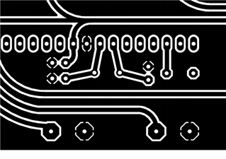
I have a direct to board print setup. That is, I print directly on the copper clad, straight out of Eagle. I have noticed that the fill lines are showing. I have found where others have had this issue, but I have not understood what to do to resolve the problem. This problem also occurs when I print the PCB to pdf format. I have read that it has to do with Eagle using lines to cover the filled area and that changing the line width and the fill style might be helpful. But, then, there are no instructions on how to do these operations and no feedback as to whether it worked, or not. Would someone please be so kind as to tell me the definitive cure and the steps to complete the task? I would be very grateful. Eagle files and libraries are attached. The problem is very clear in the pdf format. Thank you very much for your help.

Attachments:
Oscilloscope.zip
  • Sign in to reply
  • Cancel

Top Replies

  • clem57
    clem57 over 10 years ago +1
    Maybe you need to do a Polygon command setting the color. See PCB Creation with Eagle for Beginners : The Ground Plane There is more about polygon HOW-TO: Polygons and ground fills for PCBs in Eagle |…
  • balearicdynamics
    balearicdynamics over 10 years ago +1
    t1d I have downloaded the attached zip file and opened it on eagle checking for the schematics you included in PDF. The point is that the pdf is different than the schematics you attached, as in the image…
  • Bertl
    Bertl over 10 years ago in reply to balearicdynamics +1
    If you press the button "Ratsnest" (first one in the last button section, the one with the connected nodes), you will see that the area enclosed by the dashed line will fill up (flood) the free space around…
  • clem57
    0 clem57 over 10 years ago

    Maybe you need to do a Polygon command setting the color. See PCB Creation with Eagle for Beginners : The Ground Plane

    There is more about polygon HOW-TO: Polygons and ground fills for PCBs in Eagle | Dangerous Prototypes


    clem

    • Cancel
    • Vote Up +1 Vote Down
    • Sign in to reply
    • Verify Answer
    • Cancel
  • Former Member
    0 Former Member over 10 years ago in reply to clem57

    Hi, Clem, Thank you for trying to help me.


    I believe that I am creating the polygons correctly. The color of the fill is determined by the color of the layer on which the polygon is placed.


    The different layer colors are for visualization purposes. To print, I check the black box and everything prints in black. However, the polygons, which are supposed to be filled solid, have striations in them.


    Striations are lines of thicker (more ink) and thinner (less ink) ink coverage. The thinner ink lines are prone to cause etching failures.


    Eagle uses lines to fill polygons. That is to say that the fill of the polygon, which appears to be solid, is actually created with stacks of lines. When the lines are overlapping properly, the polygon appears, to the eye, to be solid. The fill lines in my polygons are not overlapping properly. So, I need to discover how to fix the overlap.


    Thanks for your interest!

    • Cancel
    • Vote Up 0 Vote Down
    • Sign in to reply
    • Verify Answer
    • Cancel
  • clem57
    0 clem57 over 10 years ago in reply to Former Member

    Is this an issue? http://www.element14.com/community/thread/17442/l/why-does-eagle-print-everything-thicker

    But if you are using a PDF see this http://indesignsecrets.com/when-you-see-thin-white-lines-in-your-pdf-files.php

    Clem

    • Cancel
    • Vote Up 0 Vote Down
    • Sign in to reply
    • Verify Answer
    • Cancel
  • balearicdynamics
    0 balearicdynamics over 10 years ago

    t1d


    I have downloaded the attached zip file and opened it on eagle checking for the schematics you included in PDF. The point is that the pdf is different than the schematics you attached, as in the image below. Maybe I am wrong interpreting the files? In eagle there is no polygon at all so the only thing I see is that you printed the PCB layout in negative At this point in your negative pdf I see that there are a couple of pads that has something that is not part of the eagle layout at all. No idea if your version of eagle make it automatically but it seems I am seeing two things.


    It is not clear what method or script are you using to generate this output layout.

    image


    My personal impression is that in the (program? script? some other else?) you are using to produce the printout generates the the disturb in the background because of some bug/issue in the script or in the settings. Initially the issue you mentioned I though maybe depending on the printer but then (see the screenshot above) you can see that seeing the image at this resolution also in the pdf the same issue appears. So it is not the printer but it is the generating application, AFAIK.image


    In the small detail you can see in this other screenshot I note that there are the pads that has a small straight connection to the rest of the background; this is what I means that the pdf output that you attached is different than the PCB layout. Should I suppose that this has been created by the program you are using for direct printing? Why? How?


    Anyway I have put on all the PCB layers and I have not saw this in the design at all.


    Take a look to the kind of image I have obtained exporting your pcb as I see it.


    image

    • Cancel
    • Vote Up +1 Vote Down
    • Sign in to reply
    • Verify Answer
    • Cancel
  • Bertl
    0 Bertl over 10 years ago in reply to balearicdynamics

    If you press the button "Ratsnest" (first one in the last button section, the one with the connected nodes), you will see that the area enclosed by the dashed line will fill up (flood) the free space around the traces and make connections to pads of the same net.


    Best,

    Herbert

    • Cancel
    • Vote Up +1 Vote Down
    • Sign in to reply
    • Verify Answer
    • Cancel
  • Former Member
    0 Former Member over 10 years ago in reply to clem57

    Thank you, Clem, for your continued support. Of the two links you provided:

    1) The first identifies a problem of spreading ink, due to using the heat transfer method, when the traces, and their clearances, are very small.

    2) The second identifies a problem of striations in the fill, but it only occurs in exported pdf files. The solution was outside of Eagle and with a different method, TBICT. They also increased the dpi, which I have done, prior; I'm using 1200 dpi and still getting the problem. It also happens, regardless of what printer that I am using.

    • Cancel
    • Vote Up 0 Vote Down
    • Sign in to reply
    • Verify Answer
    • Cancel
  • Former Member
    0 Former Member over 10 years ago in reply to balearicdynamics

    Thank you, Enrico, for your help. Wow, you have some great skills of merging text with pictures that I have never seen on a forum posting. Herbert is correct, when you open the board file within Eagle, you need to activate the RatsNest feature to fill the polygon. You can also use the layer function to manipulate the view, for other various purposes.

    • Cancel
    • Vote Up 0 Vote Down
    • Sign in to reply
    • Verify Answer
    • Cancel
  • Former Member
    0 Former Member over 10 years ago in reply to Bertl

    Hi, Herbert, thank you so much for helping me. You are correct, in regard to the RatsNest function.

    • Cancel
    • Vote Up 0 Vote Down
    • Sign in to reply
    • Verify Answer
    • Cancel
  • balearicdynamics
    0 balearicdynamics over 10 years ago in reply to Bertl

    Bertl thans for the info! You don't know but you have saved me a lot of time image


    Cheers. Enrico

    • Cancel
    • Vote Up 0 Vote Down
    • Sign in to reply
    • Verify Answer
    • Cancel
  • Bertl
    0 Bertl over 10 years ago in reply to Former Member

    Btw, not sure what your goal is, but if you want something to transfer to your board or present in a document, why not create Gerbers from your layout (File -> CAM Processor) and print them from a Gerber viewer (e.g. gerbv)?


    Best,

    Herbert

    • Cancel
    • Vote Up 0 Vote Down
    • Sign in to reply
    • Verify Answer
    • Cancel
>
element14 Community

element14 is the first online community specifically for engineers. Connect with your peers and get expert answers to your questions.

  • Members
  • Learn
  • Technologies
  • Challenges & Projects
  • Products
  • Store
  • About Us
  • Feedback & Support
  • FAQs
  • Terms of Use
  • Privacy Policy
  • Legal and Copyright Notices
  • Sitemap
  • Cookies

An Avnet Company © 2025 Premier Farnell Limited. All Rights Reserved.

Premier Farnell Ltd, registered in England and Wales (no 00876412), registered office: Farnell House, Forge Lane, Leeds LS12 2NE.

ICP 备案号 10220084.

Follow element14

  • X
  • Facebook
  • linkedin
  • YouTube