


Hey Guys,
maybe someone could give me some advice how to create a pad with two drills.
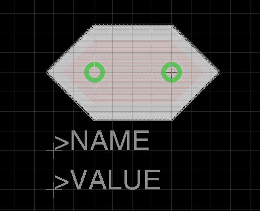
So my question is how i can create a package of a pad with two drills as illustrated in the picture below.
I thought about takeing a polygon with the right shape and placing two drills inside. As well creating a CREAM shape around it.
Maybe someone could give me some advice.

Greetings!


