element14 Community
element14 Community
    Register Log In
  • Site
  • Search
  • Log In Register
  • Community Hub
    Community Hub
    • What's New on element14
    • Feedback and Support
    • Benefits of Membership
    • Personal Blogs
    • Members Area
    • Achievement Levels
  • Learn
    Learn
    • Ask an Expert
    • eBooks
    • element14 presents
    • Learning Center
    • Tech Spotlight
    • STEM Academy
    • Webinars, Training and Events
    • Learning Groups
  • Technologies
    Technologies
    • 3D Printing
    • FPGA
    • Industrial Automation
    • Internet of Things
    • Power & Energy
    • Sensors
    • Technology Groups
  • Challenges & Projects
    Challenges & Projects
    • Design Challenges
    • element14 presents Projects
    • Project14
    • Arduino Projects
    • Raspberry Pi Projects
    • Project Groups
  • Products
    Products
    • Arduino
    • Avnet & Tria Boards Community
    • Dev Tools
    • Manufacturers
    • Multicomp Pro
    • Product Groups
    • Raspberry Pi
    • RoadTests & Reviews
  • About Us
  • Store
    Store
    • Visit Your Store
    • Choose another store...
      • Europe
      •  Austria (German)
      •  Belgium (Dutch, French)
      •  Bulgaria (Bulgarian)
      •  Czech Republic (Czech)
      •  Denmark (Danish)
      •  Estonia (Estonian)
      •  Finland (Finnish)
      •  France (French)
      •  Germany (German)
      •  Hungary (Hungarian)
      •  Ireland
      •  Israel
      •  Italy (Italian)
      •  Latvia (Latvian)
      •  
      •  Lithuania (Lithuanian)
      •  Netherlands (Dutch)
      •  Norway (Norwegian)
      •  Poland (Polish)
      •  Portugal (Portuguese)
      •  Romania (Romanian)
      •  Russia (Russian)
      •  Slovakia (Slovak)
      •  Slovenia (Slovenian)
      •  Spain (Spanish)
      •  Sweden (Swedish)
      •  Switzerland(German, French)
      •  Turkey (Turkish)
      •  United Kingdom
      • Asia Pacific
      •  Australia
      •  China
      •  Hong Kong
      •  India
      •  Korea (Korean)
      •  Malaysia
      •  New Zealand
      •  Philippines
      •  Singapore
      •  Taiwan
      •  Thailand (Thai)
      • Americas
      •  Brazil (Portuguese)
      •  Canada
      •  Mexico (Spanish)
      •  United States
      Can't find the country/region you're looking for? Visit our export site or find a local distributor.
  • Translate
  • Profile
  • Settings
Autodesk EAGLE
  • Products
  • More
Autodesk EAGLE
EAGLE User Support (English) unpopulated 4 layer board came back shorted between 3v3 and gnd. Cannot find the issue
  • Blog
  • Forum
  • Documents
  • Events
  • Polls
  • Files
  • Members
  • Mentions
  • Sub-Groups
  • Tags
  • More
  • Cancel
  • New
Join Autodesk EAGLE to participate - click to join for free!
Actions
  • Share
  • More
  • Cancel
Forum Thread Details
  • Replies 15 replies
  • Subscribers 180 subscribers
  • Views 2403 views
  • Users 0 members are here
Related

unpopulated 4 layer board came back shorted between 3v3 and gnd. Cannot find the issue

frippe75
frippe75 over 6 years ago

Hi!


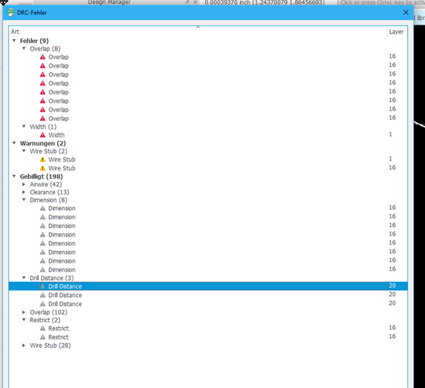
The board has a short between 3v3 and gnd and I cannot find it using drc/erc.

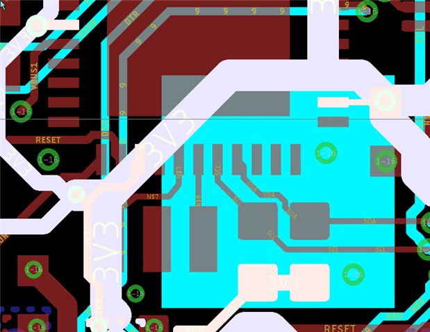
I have overlaps for sure. Those are mainly due to me drilling in pads. I have gone through all overlaps related to gnd and 3v3 signals.


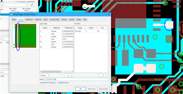
The dru is from OSHpark and their published tolerances for a 4layer board.

Tried measuing resistance on board but maybe my multimeter is too simple to show anything. But since the board is not populated and still shorted thats a bad idea.


From a schematic perspective the 3v3 and gnd cannot be shorted since they are not connected. Has to be on the board side, right?


Trying to determine if I should go back to OSHpark or not. Got three copies and they are the same so thinking this is a design issue more than anything else.


Any ideas?

  • Sign in to reply
  • Cancel

Top Replies

  • autodeskguest
    autodeskguest over 6 years ago in reply to frippe75 +4
    On 17/02/2019 18:25, Fredrik Tarnell wrote: Thanks Jan. Uploaded the brd file to my github https://github.com/frippe75/Medbee I think this is your problem. The DRC caught it but you've ignored so many…
  • Jan Cumps
    Jan Cumps over 6 years ago +3
    If you have access to a themal camera, you can put a power supply that has current control on the two lines. Either the heat will show up on the camera and indicate where the short is, or the current will…
  • autodeskguest
    autodeskguest over 6 years ago in reply to frippe75 +3
    On 17/02/2019 21:18, Fredrik Tarnell wrote: Hi Rob, Just think I ignored them in general or a particular one. They are (from a brief look) all 1-16 vias, which connect all layers. The particular one I…
  • autodeskguest
    autodeskguest over 6 years ago in reply to frippe75

    On 17/02/2019 21:18, Fredrik Tarnell wrote:

    Hi Rob,


    Just think I ignored them in general or a particular one.


    They are (from a brief look) all 1-16 vias, which connect all layers.

    The particular one I highlighted is in a 3V3 pad on layer 1 and a GND

    pad on layer 16. That makes a dead short from 3V3 to ground.


    Have been ignoring the overlaps due to drill in pads and close to pads.


    Drill in pad is generally a bad idea, which is why you get the warnings.

    It is possible to assemble boards with via in pad as long as they are

    micro-vias, but if you put a normal sized via in a pad you are asking

    for serious problems.


    But they are the same signals. Could it be that I'm chasing one via which is "infront" of a another via or something similar?


    Like I said, the specific via I highlighted absolutely is NOT the same

    signals in all layers.


    • Cancel
    • Vote Up +3 Vote Down
    • Sign in to reply
    • Cancel
  • geralds
    geralds over 6 years ago in reply to frippe75

    Hi

    I think you have design rules problems.

    image

    You've set the via from L1 to L16 but your power 3V3 goes to L2. That causes an overlap on this pin.

    Here you either have to put the Via only between L1 and L2 - Layer Settings, or a blocking area on the L16 make sure that the GND area (polygon) does not short here.

    image


    Then you have approved a lot of mistakes that are not! may be approved.

    image


    They are e.g. air wires, wire stubs, restricts, distances, clearance

    Wire stubs can be approved if they are not too close to the neighboring tracks.

    Also check the part names and labels especially on the holes and components.

    You can adjust the font sizes and styles to avoid overlapping the holes.


    This was a first check. Please make the ERC and the DRC so often that it fits and no approval is needed.

    Graphical details in the part borders can be switched off, but it is worthwhile if these are also checked.

    You can set this in the design rules, or activate in the menus.


    Best Regards

    Gerald

    ---

    • Cancel
    • Vote Up +2 Vote Down
    • Sign in to reply
    • Cancel
  • frippe75
    frippe75 over 6 years ago in reply to autodeskguest

    Thanks Jan for looking into this. Early morning so I will go about this today (looking at feedback).
    I did match the length of the diff pair (renaming them to D_P and D_N) match the length to 100% vs 100%).
    And placed ferrites close to USB receptable. Realize more rules goes into this I.e what goes underneath and so forth.
    It's a bit of a learning curve for sure!

    image

    • Cancel
    • Vote Up 0 Vote Down
    • Sign in to reply
    • Cancel
  • frippe75
    frippe75 over 6 years ago in reply to geralds

    Seriuosly Awesome Gerald!!!


    I mean could I send you a gift I would!
    I know there where a lot of DRC findings on the board.
    Airwires:
    I was too lazy here for sure, If I find these really short airwires I just confirm the routed line is on the pad (I.e copper i solid)
    Must be something in the way I work with Eagle that leave this small gaps. I think Its related to how I place the (micro)vias in pads.
    I have done two layer boards for a year of so and for me plating (tenting the via?) is not an issue. I do know these holes will suck down solder.
    And a few of my smaller components on this board has thermalpads where these 4-5 microvias actually make up a significant area of the pad.
    I try to fill them my self prior to applying solder via stencils. These are one-off's so I assemble the board manually. For production runs I would either not place them in pads or go for more expensive manufacturing where vias are tented(plated)

    Clearances:

    I'd like to think I addressed all clearances not related to vias in pads. But CLEARLY you found one I must have "passed" in a hurry. Will never do that again!

    Restricts:There is a ESP32 with onboard antenna therefor having the restrict on the toppart of the board. I have a few components that simply have to be there. Tried to avoid that area to my best abillity.
    This will affect the signal reach for sure. But ok.

    About DRC/ERC rules. They are all coming from OSHPark and I just come to realize maybe only to use them as guides and maybe nudge here and there (upwards).
    Maybe have an OSHPark-lay-original and a OSHPark-4lay-safe file.

    OSHPark does not allow for any other than drilling through layer 1-16. No blind or burried vias so I probably wont be doing these types of board anytime soon. Simply too expensive for iterative oneoff's on a budget :-)

    I will un-clear all my errors and pass them with more care this time. I think I would have miss that 3v3 drill straight into the thermal :-)


    Thanks Gerard!!!

    • Cancel
    • Vote Up +1 Vote Down
    • Sign in to reply
    • Cancel
  • autodeskguest
    autodeskguest over 6 years ago

    Am 17.02.19 um 16:24 schrieb Fredrik Tarnell:

    Hi!

    Tried measuing resistance on board but maybe my multimeter is too simple to show anything. But since the board is not populated and still shorted thats a bad idea.


    There is a simple but effective way to locate such shorts (also

    defective parts like shorted caps on populated boards:


    Take a laboratory power supply and inject a healthy but not damaging

    current into the short – here, say 1-2 amps.


    (If looking for a short on, say, a narrow thin trace pair, of course

    limit the current to maybe 0.1 amps, whatever the trace will survive.)


    Take a sensitive millivoltmeter (0.1 mV resolution or better) and start

    measuring voltage differences randomly across the board.


    The current causes a perceptible voltage drop along traces and even

    across ground planes, so you should soon find the place where the drop

    is steepest and the current is sinking into the short.


    Good luck!  Hans


    • Cancel
    • Vote Up +3 Vote Down
    • Sign in to reply
    • Cancel
<
element14 Community

element14 is the first online community specifically for engineers. Connect with your peers and get expert answers to your questions.

  • Members
  • Learn
  • Technologies
  • Challenges & Projects
  • Products
  • Store
  • About Us
  • Feedback & Support
  • FAQs
  • Terms of Use
  • Privacy Policy
  • Legal and Copyright Notices
  • Sitemap
  • Cookies

An Avnet Company © 2025 Premier Farnell Limited. All Rights Reserved.

Premier Farnell Ltd, registered in England and Wales (no 00876412), registered office: Farnell House, Forge Lane, Leeds LS12 2NE.

ICP 备案号 10220084.

Follow element14

  • X
  • Facebook
  • linkedin
  • YouTube