element14 Community
element14 Community
    Register Log In
  • Site
  • Search
  • Log In Register
  • Community Hub
    Community Hub
    • What's New on element14
    • Feedback and Support
    • Benefits of Membership
    • Personal Blogs
    • Members Area
    • Achievement Levels
  • Learn
    Learn
    • Ask an Expert
    • eBooks
    • element14 presents
    • Learning Center
    • Tech Spotlight
    • STEM Academy
    • Webinars, Training and Events
    • Learning Groups
  • Technologies
    Technologies
    • 3D Printing
    • FPGA
    • Industrial Automation
    • Internet of Things
    • Power & Energy
    • Sensors
    • Technology Groups
  • Challenges & Projects
    Challenges & Projects
    • Design Challenges
    • element14 presents Projects
    • Project14
    • Arduino Projects
    • Raspberry Pi Projects
    • Project Groups
  • Products
    Products
    • Arduino
    • Avnet & Tria Boards Community
    • Dev Tools
    • Manufacturers
    • Multicomp Pro
    • Product Groups
    • Raspberry Pi
    • RoadTests & Reviews
  • About Us
    About the element14 Community
  • Store
    Store
    • Visit Your Store
    • Choose another store...
      • Europe
      •  Austria (German)
      •  Belgium (Dutch, French)
      •  Bulgaria (Bulgarian)
      •  Czech Republic (Czech)
      •  Denmark (Danish)
      •  Estonia (Estonian)
      •  Finland (Finnish)
      •  France (French)
      •  Germany (German)
      •  Hungary (Hungarian)
      •  Ireland
      •  Israel
      •  Italy (Italian)
      •  Latvia (Latvian)
      •  
      •  Lithuania (Lithuanian)
      •  Netherlands (Dutch)
      •  Norway (Norwegian)
      •  Poland (Polish)
      •  Portugal (Portuguese)
      •  Romania (Romanian)
      •  Russia (Russian)
      •  Slovakia (Slovak)
      •  Slovenia (Slovenian)
      •  Spain (Spanish)
      •  Sweden (Swedish)
      •  Switzerland(German, French)
      •  Turkey (Turkish)
      •  United Kingdom
      • Asia Pacific
      •  Australia
      •  China
      •  Hong Kong
      •  India
      •  Japan
      •  Korea (Korean)
      •  Malaysia
      •  New Zealand
      •  Philippines
      •  Singapore
      •  Taiwan
      •  Thailand (Thai)
      •  Vietnam
      • Americas
      •  Brazil (Portuguese)
      •  Canada
      •  Mexico (Spanish)
      •  United States
      Can't find the country/region you're looking for? Visit our export site or find a local distributor.
  • Translate
  • Profile
  • Settings
Autodesk EAGLE
  • Products
  • More
Autodesk EAGLE
Forum Have a question about CadSoft EAGLE?  Ask our Expert, Richard! (Archive)
  • Blog
  • Forum
  • Documents
  • Events
  • Polls
  • Files
  • Members
  • Mentions
  • Sub-Groups
  • Tags
  • More
  • Cancel
  • New
Join Autodesk EAGLE to participate - click to join for free!
Actions
  • Share
  • More
  • Cancel
Forum Thread Details
  • Replies 1129 replies
  • Subscribers 245 subscribers
  • Views 51115 views
  • Users 0 members are here
  • eagle
  • expert
  • richard_hammerl
  • cadsoft
Related

Have a question about CadSoft EAGLE?  Ask our Expert, Richard! (Archive)

nlarson
nlarson over 16 years ago

This thread is now locked - but you can still ask Richard by posting your questions here.  If you'd rather browse other member's questions you can read the CadSoft EAGLE Forums for past questions and answers. Enjoy!


Browse past Q&A help on anything technical relating to CadSoft EAGLE!


image


Richard Hammerl

Richard is an engineer with 16 years experience in EAGLE customer support and is waiting for your questions.

  • Sign in to reply
  • Cancel
  • e14 Contributor
    e14 Contributor over 14 years ago

    Hi,


    I am trying to make a carrier board for a SOM with multiple connectors. Specifically a SOM OMAP-L138: http://www.logicpd.com/products/system-on-modules/omap-l138-som-m1/


    The  SOM is using 3 hirose connectors to connect to the carrier board. As the connectors need to be placed very precisely, they recommend machine placement.


    How  do you create an eagle device with three connectors that also generates  the neccessary pick-and-place information? I have made a device  already, but it has only one package which includes all 3 connectors, and pick-and-place information is generated per-package.


    Do  I really need to make 3 separate devices for the 3 connectors and then  manually place them during board layout? That is a bit of a pain when  having to move the device around.


    Nikolaj

    • Cancel
    • Vote Up 0 Vote Down
    • Sign in to reply
    • Cancel
  • e14 Contributor
    e14 Contributor over 14 years ago in reply to e14 Contributor

    I´ve just read a thread (http://www.element14.com/community/thread/4068?start=0&tstart=0) where some people have problems with design link, but it appears to be another kind of problems (unexpected end of file, so they have established a communication with the server) but my error is a "handshake error".


    So I have no idea about the problem.


    I would thank any help,


    Regards,


    Xabier Aldecoa.

    Ariadna Instruments.

    • Cancel
    • Vote Up 0 Vote Down
    • Sign in to reply
    • Cancel
  • Richard_H
    Richard_H over 14 years ago in reply to e14 Contributor

    Hi Craig,


    this is a known problem which is fixed in EAGLE 6.1.0. Please download it from our web site

    http://www.cadsoft.de/downloads/


    Regards,

    Richard

    • Cancel
    • Vote Up 0 Vote Down
    • Sign in to reply
    • Cancel
  • Richard_H
    Richard_H over 14 years ago in reply to e14 Contributor

    Hi Rachad,


    could you please check whether the files are consistent (ERC command) ? Maybe the board file was not loaded while you drew the nets in the schematic....


    Regards,

    Richard

    • Cancel
    • Vote Up 0 Vote Down
    • Sign in to reply
    • Cancel
  • e14 Contributor
    e14 Contributor over 14 years ago in reply to Richard_H

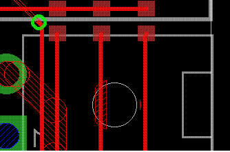
    I made a library part with a hole in it.

    After I place this part into my schematic,

    the auto-router is routing traces right through the hole?

    I see the hole is in the DIMENSION LAYER?

    Any idea why the autorouter is doing this?

    image

    • Cancel
    • Vote Up 0 Vote Down
    • Sign in to reply
    • Cancel
  • e14 Contributor
    e14 Contributor over 14 years ago

    hello Mr. Richard,


    would like to ask about the BUS button.

    i used this command to draw a blue thick line representing a group of nets. I named this bus with the following : PORTC[0..7].

    i used the 'NET' button to start drawing the nets between the bus and the corresponding components pins.

    in the schematic i could see the physical connection , but in the board file ( '.brd' file ) i can't see this connection.


    what could be the reason for that ?


    thank you for your time

    • Cancel
    • Vote Up 0 Vote Down
    • Sign in to reply
    • Cancel
  • e14 Contributor
    e14 Contributor over 14 years ago in reply to Richard_H

    Yes. Very nice!

    • Cancel
    • Vote Up 0 Vote Down
    • Sign in to reply
    • Cancel
  • Richard_H
    Richard_H over 14 years ago in reply to e14 Contributor

    Hi,


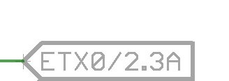
    just want to add that the connection itself is made by the net name. Nets with the same name are connected.

    It is not neccessary to have labels (simple or xref), but of course it is nice to have. image


    Regards,

    Richard

    • Cancel
    • Vote Up 0 Vote Down
    • Sign in to reply
    • Cancel
  • e14 Contributor
    e14 Contributor over 14 years ago in reply to e14 Contributor

    You should name the wires with the same name. Then you can add a label, and change the cross-reference option to ON rather than PLAIN (you can do this with the 'i' or info button, then clicking on the label to bring up the options). That will give you a label as shown in the attached image, where it shows you the wire's name and the location on the other sheet.

    image

    • Cancel
    • Vote Up 0 Vote Down
    • Sign in to reply
    • Cancel
  • e14 Contributor
    e14 Contributor over 14 years ago

    I have two sheets in my schematic editor and I need to have wires/networks span from one sheet to another. How do I link the wires together.  Is there some sort of port symbol that will do this?

    • Cancel
    • Vote Up 0 Vote Down
    • Sign in to reply
    • Cancel
<>
element14 Community

element14 is the first online community specifically for engineers. Connect with your peers and get expert answers to your questions.

  • Members
  • Learn
  • Technologies
  • Challenges & Projects
  • Products
  • Store
  • About Us
  • Feedback & Support
  • FAQs
  • Terms of Use
  • Privacy Policy
  • Legal and Copyright Notices
  • Sitemap
  • Cookies

An Avnet Company © 2026 Premier Farnell Limited. All Rights Reserved.

Premier Farnell Ltd, registered in England and Wales (no 00876412), registered office: Farnell House, Forge Lane, Leeds LS12 2NE.

Follow element14

  • X
  • Facebook
  • linkedin
  • YouTube