element14 Community
element14 Community
    Register Log In
  • Site
  • Search
  • Log In Register
  • About Us
  • Community Hub
    Community Hub
    • What's New on element14
    • Feedback and Support
    • Benefits of Membership
    • Personal Blogs
    • Members Area
    • Achievement Levels
  • Learn
    Learn
    • Ask an Expert
    • eBooks
    • element14 presents
    • Learning Center
    • Tech Spotlight
    • STEM Academy
    • Webinars, Training and Events
    • Learning Groups
  • Technologies
    Technologies
    • 3D Printing
    • FPGA
    • Industrial Automation
    • Internet of Things
    • Power & Energy
    • Sensors
    • Technology Groups
  • Challenges & Projects
    Challenges & Projects
    • Design Challenges
    • element14 presents Projects
    • Project14
    • Arduino Projects
    • Raspberry Pi Projects
    • Project Groups
  • Products
    Products
    • Arduino
    • Avnet Boards Community
    • Dev Tools
    • Manufacturers
    • Multicomp Pro
    • Product Groups
    • Raspberry Pi
    • RoadTests & Reviews
  • Store
    Store
    • Visit Your Store
    • Choose another store...
      • Europe
      •  Austria (German)
      •  Belgium (Dutch, French)
      •  Bulgaria (Bulgarian)
      •  Czech Republic (Czech)
      •  Denmark (Danish)
      •  Estonia (Estonian)
      •  Finland (Finnish)
      •  France (French)
      •  Germany (German)
      •  Hungary (Hungarian)
      •  Ireland
      •  Israel
      •  Italy (Italian)
      •  Latvia (Latvian)
      •  
      •  Lithuania (Lithuanian)
      •  Netherlands (Dutch)
      •  Norway (Norwegian)
      •  Poland (Polish)
      •  Portugal (Portuguese)
      •  Romania (Romanian)
      •  Russia (Russian)
      •  Slovakia (Slovak)
      •  Slovenia (Slovenian)
      •  Spain (Spanish)
      •  Sweden (Swedish)
      •  Switzerland(German, French)
      •  Turkey (Turkish)
      •  United Kingdom
      • Asia Pacific
      •  Australia
      •  China
      •  Hong Kong
      •  India
      •  Korea (Korean)
      •  Malaysia
      •  New Zealand
      •  Philippines
      •  Singapore
      •  Taiwan
      •  Thailand (Thai)
      • Americas
      •  Brazil (Portuguese)
      •  Canada
      •  Mexico (Spanish)
      •  United States
      Can't find the country/region you're looking for? Visit our export site or find a local distributor.
  • Translate
  • Profile
  • Settings
Altium CircuitStudio
  • Products
  • Manufacturers
  • Altium CircuitStudio
  • More
  • Cancel
Altium CircuitStudio
Altium CircuitStudio Forum polygon region short circuit
  • Blog
  • Forum
  • Documents
  • Events
  • Polls
  • Members
  • Mentions
  • Sub-Groups
  • Tags
  • More
  • Cancel
  • New
Join Altium CircuitStudio to participate - click to join for free!
Actions
  • Share
  • More
  • Cancel
Forum Thread Details
  • Locked Locked
  • Replies 23 replies
  • Subscribers 88 subscribers
  • Views 5012 views
  • Users 0 members are here
Related
This discussion has been locked.
You can no longer post new replies to this discussion. If you have a question you can start a new discussion

polygon region short circuit

acw210ee
acw210ee over 2 years ago

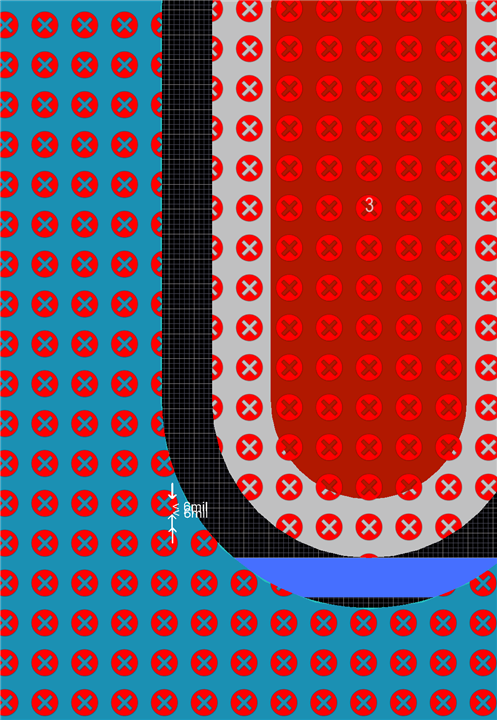
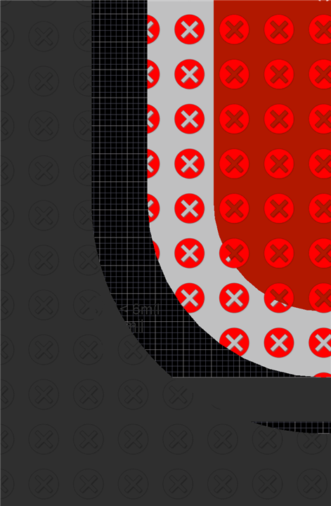
So i have polygons overlapping each other connected to nets, it seemed to draw them fine with J1 in the pcb however i get the DRC i get a short errors:

Clearance Constraint (Gap=6mil) (All),(All)
Polygon Region (93 hole(s)) Bottom Layer Pad J1-1(2129.921mil,-459.134mil) Multi-Layer
Polygon Region (88 hole(s)) Signal Layer 2 Pad J1-1(2129.921mil,-459.134mil) Multi-Layer
Polygon Region (93 hole(s)) Bottom Layer Pad J1-3(1870.079mil,-459.134mil) Multi-Layer
Polygon Region (88 hole(s)) Signal Layer 2 Pad J1-3(1870.079mil,-459.134mil) Multi-Layer
Polygon Region (48 hole(s)) Top Layer Pad J1-3(1870.079mil,-459.134mil) Multi-Layer


Back to top

Short-Circuit Constraint (Allowed=No) (All),(All)
Polygon Region (93 hole(s)) Bottom Layer Pad J1-3(1870.079mil,-459.134mil) Multi-Layer
Polygon Region (88 hole(s)) Signal Layer 2 Pad J1-3(1870.079mil,-459.134mil) Multi-Layer
Polygon Region (48 hole(s)) Top Layer Pad J1-3(1870.079mil,-459.134mil) Multi-Layer

When i remove J1 the problem goes away, however i am not sure what is causing it. As the issue with the polygon pours does not occur with the ot

her components. Should i just ignore the issue?

image

  • Cancel
Parents
  • GabeFromSpace
    GabeFromSpace over 2 years ago

    As Shabaz said, DRC errors should not be ignored unless the reason is known and acknowledged. Which layers of your PCB have polygons on them and which nets are they connected to?

    Having 2 overlapping polygons on the same layer with different nets is generally a "no no". If you have to have polygons on the same layer with different nets, they shouldn't be overlapping.

    • Cancel
    • Vote Up 0 Vote Down
    • Cancel
  • charlieo21
    charlieo21 over 2 years ago in reply to GabeFromSpace

    Overlapping polygons is not a problem because when they are poured, they follow the design rules. My guess is that you need to repour the polygons.

    • Cancel
    • Vote Up 0 Vote Down
    • Cancel
  • acw210ee
    acw210ee over 2 years ago in reply to acw210ee

     image

    I think this might be an error with circuit studio. As when i move the copper plane away like this the drc errors go away (you can see the polygons are still overlapping on other parts of the pcb and i get no DRC error). However when i move that copper polygon (which is connected to ground) back over J1 the errors come back for pin 3 (no connect) and pin 1 (12V).

    • Cancel
    • Vote Up 0 Vote Down
    • Cancel
  • GabeFromSpace
    GabeFromSpace over 2 years ago in reply to shabaz

    The trace indicated by the orange arrow is on a mechanical layer and shouldn't interact with the Short circuit part of the DRC. It's meant for the design stage and shouldn't show up in the gerbers. the light gray area is a multi-layer pad, meaning it's a pad on the top, inner, and bottom layers. The red pad is a *hopefully plated slot. The silkscreen is the lighted traces on the footprint. That being said, exporting a gerber file and opening it up in a separate viewer like Gerbview would be a good idea at this point.

    • Cancel
    • Vote Up 0 Vote Down
    • Cancel
  • charlieo21
    charlieo21 over 2 years ago in reply to shabaz

    The DRC errors points to pads 1 & 3, apparently the GND polygon is touching those pads.

    acw210ee try closing CS, opening again, repour all the polygons, run DRC again.

    • Cancel
    • Vote Up 0 Vote Down
    • Cancel
  • acw210ee
    acw210ee over 2 years ago in reply to shabaz

    i looked at those traces and those are on the "top overlay" in the pcb footprint. whats interesting is i get no error for pin 5 when i do the drc only pins 1 and 3

    • Cancel
    • Vote Up 0 Vote Down
    • Cancel
  • GabeFromSpace
    GabeFromSpace over 2 years ago in reply to charlieo21

    ^ I second this.

    I've also had a buggy install of CS before. If the gerber files look good, and all else fails, it might not hurt to uninstall and reinstall it.

    • Cancel
    • Vote Up 0 Vote Down
    • Cancel
  • charlieo21
    charlieo21 over 2 years ago in reply to acw210ee

    You can try putting a polygon pour cutout in the same area of those pads and see if the DRC error goes away.

    • Cancel
    • Vote Up 0 Vote Down
    • Cancel
  • acw210ee
    acw210ee over 2 years ago in reply to charlieo21

    Re-opening did not fix the issue. I was able to fix it by messing around with the design rules. It seems it has an issue routing polygons around slot shaped pins. Essentially in design rules, electrical, clearance, i changed the polygon minimum clearances to 10 mils for everything. Repoured the polygons, then changed the design rules back to 6 mils, then did not repour the polygons and did a DRC check. That removed the short circuit errors, however i still have 3 clearance errors. image

    it is where that 6 mil white mark is, there is nothing there to even be "clear" of so it makes no sense so I am going to ignore it. Overall i think the root cause is circuitstudio has some issues with the design rules when pouring polygons around slot shaped pads. 

    • Cancel
    • Vote Up 0 Vote Down
    • Cancel
  • GabeFromSpace
    GabeFromSpace over 2 years ago in reply to acw210ee

    It's always been fine for me.

    image

    Can you go under "view", select "single layer mode", and take screenshots of the same area on each copper layer? It might be referring to something on a different layer.

    • Cancel
    • Vote Up 0 Vote Down
    • Cancel
  • acw210ee
    acw210ee over 2 years ago in reply to GabeFromSpace

    imageimageimageimageimage

    • Cancel
    • Vote Up 0 Vote Down
    • Cancel
  • acw210ee
    acw210ee over 2 years ago in reply to acw210ee

    layers are bot, signal 1, signal 2, top

    • Cancel
    • Vote Up 0 Vote Down
    • Cancel
Reply
  • acw210ee
    acw210ee over 2 years ago in reply to acw210ee

    layers are bot, signal 1, signal 2, top

    • Cancel
    • Vote Up 0 Vote Down
    • Cancel
Children
  • shabaz
    shabaz over 2 years ago in reply to acw210ee

    It could be worth trying a clearance of (say) 6.1 mil, just in case there is more than one parameter set to the same value, and rounding error on a curve or similar causing some weird issue. For instance with EAGLE, I seem to recall the polygons would be drawn with a line width too, and it was occasionally possible for rounding issues to cause errors if multiple rules used the same value. 

    • Cancel
    • Vote Up 0 Vote Down
    • Cancel
  • GabeFromSpace
    GabeFromSpace over 2 years ago in reply to acw210ee

    It looks like you're doing everything right. I think the software is just running into some sort of bug. As long as you check the gerbers after you export them, you can probably ignore it.

    That being said, if you still want to get your DRC to pass, you could try to do some experiments like adding a different through-hole component to that area of the PCB, and seeing if the issue pops up on that one too. If it doesn't you could just try to remake the component and footprint yourself from scratch.

    • Cancel
    • Vote Up 0 Vote Down
    • Cancel
  • charlieo21
    charlieo21 over 2 years ago in reply to GabeFromSpace

    I agree, everything points to a software bug. I think putting a polygon pour cutout on those pads should avoid the DRC errors.

    • Cancel
    • Vote Up 0 Vote Down
    • Cancel
element14 Community

element14 is the first online community specifically for engineers. Connect with your peers and get expert answers to your questions.

  • Members
  • Learn
  • Technologies
  • Challenges & Projects
  • Products
  • Store
  • About Us
  • Feedback & Support
  • FAQs
  • Terms of Use
  • Privacy Policy
  • Legal and Copyright Notices
  • Sitemap
  • Cookies

An Avnet Company © 2025 Premier Farnell Limited. All Rights Reserved.

Premier Farnell Ltd, registered in England and Wales (no 00876412), registered office: Farnell House, Forge Lane, Leeds LS12 2NE.

ICP 备案号 10220084.

Follow element14

  • X
  • Facebook
  • linkedin
  • YouTube