
Welcome to the Digilent! Here you can find our latest news, videos, and product details. Additionally, you can engage with us in our forums.
The Analog Discovery Pro 2400 Series expands Digilent’s professional test and measurement lineup with a pair of USB-based mixed signal oscilloscopes designed for engineers who require higher bandwidth, deeper memory, and tight integration between analog and digital analysis, without moving to a full benchtop instrument.
The series consists of two models:
Both devices share the same hardware platform, software environment, and I/O architecture, allowing educators and engineers to select the performance profile that best fits their application while maintaining a consistent lab experience.
Modern engineering systems rarely exist in purely analog or purely digital domains. The ADP‑2400 Series addresses this by integrating:
This combination enables simultaneous analog and digital acquisition, protocol analysis, signal generation, and long-duration capture within a single instrument.
Both models support referenced single-ended inputs with selectable 50 ohm or 1 megaohm input impedance, input ranges up to ±25 V, and ten hardware input ranges that allow users to balance resolution and dynamic range depending on the measurement task.
The key distinction within the ADP‑2400 Series is how each model balances bandwidth and vertical resolution.
This configuration is well suited for applications where amplitude accuracy, noise performance, and signal fidelity are priorities.
This model targets higher-speed digital interfaces, fast edge characterization, and applications that benefit from increased bandwidth.
Both devices support deep buffer memory, complex triggering modes including edge, pulse, glitch, timeout, transition, and window triggers, and advanced visualization tools such as FFT, persistence, eye diagrams, histograms, and custom math functions.
Each ADP‑2400 Series device includes a single-channel arbitrary waveform generator offering:
Standard waveforms, advanced modulation modes, frequency and amplitude sweeps, and custom waveforms are supported. The waveform generator integrates directly with oscilloscope, network analyzer, and impedance analyzer instruments within WaveForms, enabling closed-loop measurement and characterization workflows without additional hardware.
The sixteen digital I/O channels are internally clocked and configurable for both acquisition and generation tasks. Key capabilities include:
Supported protocol analysis and generation includes SPI, I2C, UART, CAN, I2S, LIN, SWD, JTAG, HDMI CEC, SAE J1850, and additional industry-standard interfaces. These capabilities make the ADP‑2400 Series appropriate for embedded systems education, capstone projects, and early-stage product development.
The ADP‑2400 Series supports Dual Mode operation, allowing two devices to be synchronized and operated as a single system. In this configuration, users gain access to:
Automatic phase adjustment and cross-triggering allow multiple instruments to operate together without external synchronization hardware, which is particularly useful in advanced teaching labs and scalable instructional environments.
All device functionality is accessed through Digilent’s WaveForms software, available for Windows, macOS, and Linux. WaveForms provides a unified user interface that reflects traditional benchtop workflows while supporting simultaneous operation of multiple instruments.
For automation and customization, users can employ the integrated scripting environment or leverage the WaveForms SDK to create custom applications using C, C++, Python, C#, and other supported languages. This enables repeatable testing, hardware-in-the-loop setups, and integration with external systems.
The ADP‑2400 Series is housed in a metal enclosure designed for both desktop and mounted use. Hardware features include:
This form factor supports use in teaching labs, development environments, and semi-permanent test setups.
Within the Digilent test and measurement portfolio, the ADP‑2400 Series sits between Discovery Essentials devices and higher-bandwidth Analog Discovery Pro 5000 Series instruments. It is intended for users who require more bandwidth, memory depth, and I/O capability than student-focused tools provide, while maintaining the flexibility of a USB-based platform.
For academic programs, this positions the ADP‑2400 Series well for upper-division laboratories and project-based courses. For practicing engineers, it offers a compact instrument aligned with professional measurement workflows.
Digilent recently introduced the ADP5470 and ADP5490, two new models in the Analog Discovery Pro 5000 Series. Both are four-channel mixed-signal oscilloscopes with significantly higher bandwidth and sample rates than previous models. To test their capabilities, a project was built around measuring how fast Pmod I/O pins on an FPGA can switch — a key performance factor in many digital designs.
One of the most common questions in FPGA work is how fast a pin can toggle. This affects how quickly data can be transferred in and out of the board. Several factors impact this, including PCB trace length, quality of the connector, and whether current-limiting resistors are present. Pmod connectors are widely used due to their simplicity, but they don’t support the same speeds as more robust options like FMC or SYZYGY. Understanding their limitations helps with designing reliable systems.
The test was run on an Arty S7 FPGA board. The design exposed the Clocking Wizard settings through a serial interface, allowing a Python script to adjust the frequency dynamically. An ADP5490 oscilloscope was then used to capture and analyze the output waveforms on the Pmod I/O pins. The goal was to determine whether the digital signals still met the LVCMOS logic thresholds at different frequencies.
For 3.3V LVCMOS logic, a valid rising edge must go from below 0.4 V to above 2.4 V. These are the VOH and VOL thresholds defined in the Spartan 7 documentation. However, these thresholds are for static DC signals. When switching at high speeds, reflections, parasitic capacitance, and trace inductance can cause signal integrity issues. The oscilloscope was used to measure if these thresholds were still respected as the frequency increased.
At 10 MHz, the waveforms were clean, and the phase shifts between channels were close to the expected values — 0°, 45°, and 90° between different outputs. At 60 MHz, the signals still transitioned cleanly, but the waveform edges showed slower slew rates. Harmonics were visible, confirming the oscilloscope’s ability to capture high-frequency content.
At 75 MHz, the signals started showing unexpected behavior. The amplitude increased beyond the expected levels, possibly due to overshoot or ringing. Despite this, the transitions still crossed the logic thresholds. This result highlights how analog effects can start to interfere with digital signaling at higher speeds.
To understand how hardware components affect signal integrity, two different Pmod outputs were compared — one with a series resistor and one without. The scope captured clear differences in edge shape and amplitude between the two. This shows that even small changes in the signal path, like adding a resistor, can alter performance. The Scope to Digital feature in WaveForms helped confirm transitions by converting analog signals into digital logic states based on a defined threshold.
Square waves are made up of many harmonic frequencies. To capture them accurately, a scope needs much higher bandwidth than the base frequency of the signal. For example, a 75 MHz square wave can have meaningful content up to several hundred MHz. Lower-bandwidth tools like the Analog Discovery 3 may miss these harmonics, distorting the observed signal. The ADP5000 Series scopes can capture these harmonics, giving a more accurate view of what’s actually happening at the I/O pin.
All measurements were taken with only the FPGA board and the scope connected. No external modules or Pmod peripherals were attached. In a real setup, connecting other hardware would change the signal characteristics due to additional loading and parasitic effects. Results may vary depending on what’s connected to the system.
The full article includes screenshots, waveform plots, and more details on the scope settings and observations made during testing.
To read the complete post, visit: https://digilent.com/blog/characterizing-a-pmod-ports-switching-frequency-advantages-of-a-high-bandwidth-oscilloscope/
Working with a data acquisition system (DAQ) often feels straightforward—especially when you’re only measuring one channel. But once you expand beyond that and bring multiple inputs into the mix, things can get tricky. You might connect a sensor, verify its output with a multimeter like the Fluke 77, and everything seems fine. But when you try the same with your DAQ, the results suddenly don’t line up. At that point, it’s easy to assume something’s wrong with the device. But in reality, many issues stem from how DAQs handle multiple channels, and how those channels interact behind the scenes.
This article breaks down some of the most common DAQ-related issues and explains what you can do to make your measurements more reliable.
Before diving into troubleshooting, it’s worth asking a fundamental question: what kind of DAQ are you using? Specifically, does it have simultaneous inputs—where each channel has its own dedicated analog-to-digital converter (ADC)—or is it a multiplexed device that uses a single ADC to cycle through multiple inputs?
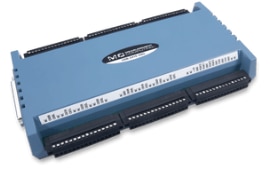
The distinction matters. Simultaneous-input DAQs, like the USB-1808X or USB-1608FS-Plus, tend to be easier to work with and more accurate in multi-channel setups. These types often use one ADC per channel, either in a single integrated chip or across multiple chips, as in the case of devices like the MCC 172 or WebDAQ 504.
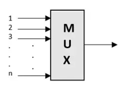
On the other hand, multiplexed DAQs—such as the USB-2416—use solid-state analog switches (MUX chips) to direct each channel sequentially to a single ADC. This approach reduces cost but introduces potential signal integrity issues due to shared circuitry and capacitance between channels.
When a DAQ cycles between inputs using multiplexing, the small internal capacitance between channels can become problematic. Each time the system switches from one signal to another, it can create a kind of ghost image of the previous signal on the next channel. This is especially noticeable if one channel is connected and its neighbor isn’t—suddenly the inactive channel picks up a residual voltage.
One way to avoid this is by making sure that all channels—especially the unused ones—are either grounded or connected to a low-impedance source (ideally under 100 ohms). This helps dissipate any leftover charge quickly and allows the new channel to settle on the correct value. High-impedance circuits like resistor dividers can complicate things, especially on multiplexed systems, and should be used with caution.
Interestingly, resistor dividers can still work well on DAQs with simultaneous inputs. But on multiplexed systems, their effectiveness depends on timing. For example, some devices offer a “Burst Mode” that scans inputs rapidly with minimal delay between channels. That short delay may not be enough time for the residual charge to dissipate, leading to inaccurate readings.
If you're using resistor dividers with a multiplexed DAQ, it helps to disable burst mode and space out the sampling rate. Doing so gives the system more time between readings and reduces interference between channels. Just be aware that some devices, like the USB-1616HS, are always in burst mode, while others, like the USB-1608G, let you turn it off when needed.
Isolation is another critical concept in DAQ accuracy. At its simplest, isolation means that there’s no direct electrical connection to earth ground. Devices that are isolated don’t share a ground path with the host computer, which helps eliminate ground loops and interference.
There are a few types of isolation. Device-level isolation separates the DAQ from the computer’s ground. If external power is used, internal transformers provide additional protection. Some DAQs go even further, offering channel-to-channel and channel-to-ground isolation, which is particularly useful when multiple signal sources or sensors might interact electrically.
A good multimeter like the Fluke 77 is battery powered, making it inherently isolated. That’s one of the reasons it’s so reliable for validating sensor readings—even in electrically noisy environments.
One of the most common causes of strange DAQ behavior is a ground loop. This occurs when multiple paths to ground exist, which can introduce unwanted voltage into the measurement system. Even a small amount of extra voltage can skew sensor readings—especially when dealing with low-voltage signals like those from thermocouples.
Thermocouples are particularly vulnerable. Grounded thermocouples, for instance, can form a loop if their sensing junction is mounted on a conductive surface. Inside the DAQ, the system automatically ties the thermocouple’s low side to the analog reference when the input is set to thermocouple mode, increasing the chance for interaction between adjacent channels.
If you suspect a ground loop involving a thermocouple and another powered sensor, you have a few options. One is to isolate the thermocouple tip using insulating materials like Kapton tape (up to 500 °F), mica washers, or other non-conductive barriers. In more complex setups where multiple grounds are unavoidable, using channel-isolated modules can solve the problem. These modules not only condition the signal but also provide galvanic isolation between each channel and the system. Brands like Dataforth offer affordable models in the 8B series, though each can add around $100–$200 per channel to your system cost.
Electrical noise is everywhere—from power grids to motors, heaters, and industrial equipment. Many DAQ systems use sigma-delta ADCs, which are tuned to suppress 50/60 Hz noise from AC mains. But once frequencies shift—say from a motor ramping up or an oven heating—the digital filters can fall short.
Sometimes the fix is as simple as relocating your DAQ system further from the source of interference. USB cables with ferrite chokes can also help dampen high-frequency noise. And once again, isolation modules prove useful, as they often include low-pass hardware filters that block unwanted frequencies more effectively than software-based solutions.
If you're unsure whether your DAQ is performing correctly, one of the easiest ways to verify is by measuring a known voltage source—like a battery. This might seem basic, but it’s an effective way to confirm that your hardware is functioning. A battery is stable, low-noise, and has low impedance—ideal for testing. If you're using a differential input, just connect a 100kΩ resistor between the low-side input and ADC ground to give the system a reference point.
Once you see that your DAQ measures the battery accurately, you can start reconnecting other signals one by one. This can help pinpoint where noise or error is creeping in. If things go wrong again, it’s often due to interference, improper grounding, or issues between channels.
Shielded wiring like coaxial cables or twisted-pair shielded wires can reduce some noise, but certain types of interference will still pass through—especially if the noise doesn’t fall within the filtering range of your ADC.
Multi-channel DAQ systems introduce a lot of moving parts, and small mistakes can quickly snowball into confusing results. Whether it’s unexpected readings due to multiplexing, signal bleed from high impedance, or elusive ground loops and noise, these systems require a deeper understanding of how inputs behave and interact.
The good news is that most of these issues have reliable solutions. Once you know what to look for—and how to isolate each component—you’ll be able to build more accurate, stable, and trustworthy measurement systems for your applications. Read the detailed blog post here.
This demonstration project is designed to showcase the use of the Zmod AWG 1411 module in combination with the Genesys ZU development board. It provides a functional starting point for anyone looking to build their own arbitrary waveform generator functionality, and it also serves as a straightforward method for verifying that the hardware setup is working as expected.
To run this demo, you’ll need either the Genesys ZU-3EG or ZU-5EV board, a MicroUSB cable, a stable power supply, and a Zmod AWG 1411 module. On the software side, the demo requires a Vivado installation compatible with version 2024.1, as well as the classic version of Vitis. At the time this was written, Digilent did not yet support the newer Vitis Unified UI, so sticking with the classic interface is essential.
The Digilent Genesys ZU is a standalone Zynq UltraScale+ EG/EV MPSoC development board, designed to provide an ideal entry point by combining cost-effectiveness with powerful multimedia and network connectivity interfaces. There are two variants of the Genesys ZU: 3EG and 5EV. These two variants are differentiated by the MPSoC chip version and some peripherals.
As with other FPGA demos from Digilent, this one is tied to specific board variants and tool versions. Each release includes the relevant files for a particular combination of board and Vivado version. For example, a release tagged for the ZU-5EV board will only work with that version and must be run using Vivado 2024.1. Older releases used a different repository structure and tag format, so users working with legacy tools will need to reference documentation specific to those versions.
Each release includes two key archives: a Vivado project in .xpr.zip format and a Vitis workspace in .ide.zip format. The Vivado archive contains the hardware design and can be opened and modified if needed, although this isn’t required just to run the demo. The Vitis archive, on the other hand, contains the software application that runs on the board. Unlike the Vivado files, this Vitis project archive should not be unzipped manually; Vitis imports it directly in its original form.
Once everything is set up, the demo runs as a simple interactive test through a serial terminal. The application cycles through four configurations: uncalibrated outputs at low range, uncalibrated outputs at high range, calibrated outputs at low range, and calibrated outputs at high range. At each stage, a ramp waveform is generated on both AWG output channels. A newline character sent via USBUART will advance the demo to the next configuration.
By connecting an oscilloscope, such as a Digilent ADP2330, to the SMA outputs, users can measure the peak-to-peak voltage of the generated signals. The output waveforms span the full digital range of the device, offering a comprehensive check of the output range across calibration and gain settings.
While running the demo requires no hardware modifications, users who want to customize or rebuild the hardware platform can do so. This involves opening the Vivado project from the release, generating a new hardware design, and exporting it as an updated platform for Vitis. The workspace structure is designed to support platform updates, including a workaround for known issues related to FSBL generation and BSP optimization.
When making these changes, users must manually replace certain initialization files and verify that paths to the FSBL ELF and XSA files are correct. The process includes rebuilding the FSBL, boot components, and the master system project, ensuring that all dependencies are properly updated after any platform changes.
The demonstration provides clear, measurable output for each configuration, giving users a solid understanding of how the AWG performs under various settings. Sample measurements show how the output range differs before and after calibration, and how gain settings affect signal amplitude. While the test data referenced is based on a factory-calibrated module from several years prior, users can expect even more accurate results with a recently calibrated unit.
Here’s an example of the kind of data the demo can produce:
| Trial / Channel | Vpk-pk (nominal) | Vpk-pk (measured) | % Error |
|---|---|---|---|
| 1. Ch1 | ~2.5 V | 2.7328 V | 9.312% |
| 1. Ch2 | ~2.5 V | 2.7451 V | 9.804% |
| 2. Ch1 | ~10.0 V | 10.493 V | 4.93% |
| 2. Ch2 | ~10.0 V | 10.573 V | 5.73% |
| 3. Ch1 | 2.5 V | 2.5092 V | 0.368% |
| 3. Ch2 | 2.5 V | 2.5236 V | 0.944% |
| 4. Ch1 | 10.0 V | 9.8621 V | 1.379% |
| 4. Ch2 | 10.0 V | 9.9391 V | 0.609% |
These values demonstrate how calibration significantly improves accuracy in both low and high output ranges.
This demo offers an effective and practical way to validate the Genesys ZU with the Zmod AWG. Whether you're looking to confirm that your board is working or planning to extend the design for more complex waveform generation tasks, this project provides a strong foundation.
For further reading, including HDL development guidance and workspace navigation in Vivado, you can explore Digilent’s resources on creating hardware designs. Technical support is also available through the Digilent FPGA Forum, where engineers and community members can help with troubleshooting or project customization.
If you’re looking for the full set of steps—such as importing the Vitis project, building software applications, or exporting hardware platforms—you’ll find all the detailed documentation on the official Genesys ZU Zmod AWG demo page on Digilent’s website.
The Analog Discovery Studio Max (ADS Max) is a versatile and comprehensive electronics laboratory solution tailored for academic environments. It integrates 14 essential test instruments, including an oscilloscope, waveform generator, logic analyzer, spectrum analyzer, digital multimeter (DMM), power supplies, and protocol analyzer, into a single device. The LabVIEW WaveForms Toolkit enables further productivity and learning with a tight integration between the data acquisition capabilities of the ADS Max with LabVIEW's extensive analysis tools in an intuitive way.
One of the standout features of the ADS Max is its ability to facilitate seamless circuit prototyping. The device includes integrated power supplies and a breadboardable interface, enabling students to easily design and test circuits. This functionality is particularly beneficial for courses focused on circuit design, signal analysis, and embedded systems, where students can experiment with real-world applications and gain a deeper understanding of engineering principles.

The ADS Max is also designed to support a wide range of learning environments, from traditional classrooms and laboratories to remote learning setups. Its compact and comprehensive nature makes it ideal for students working from home or in limited lab spaces. Additionally, the included Digilent WaveForms software offers prebuilt instrument panels for immediate use, while APIs for LabVIEW, C, and Python allow for custom software development, providing flexibility for both instructors and students.

Furthermore, the ADS Max is part of a broader ecosystem that includes the Canvas Max and other subject-specific materials developed by academic partners. This ecosystem extends the platform's capabilities, offering ready-to-use materials for labs in various engineering topics such as wireless communications, power electronics, and digital circuits. By leveraging this ecosystem, educators can create dynamic and engaging learning experiences that cater to a wide range of educational needs and objectives.
This demo project showcases a stopwatch game designed in Verilog for the Basys 3 FPGA development board . The idea behind it is simple but effective: the user presses a button to start a timer and then tries to stop it at the perfect moment. It’s a fun, hands-on way to explore essential digital design concepts like finite state machines, counters, and basic I/O handling, all implemented using a hardware description language.
The Basys 3 is one of the best boards on the market for getting started with FPGA. It is an entry-level development board built around a Xilinx Artix-7 FPGA.
As a complete and ready-to use digital circuit development platform, it includes enough switches, LEDs, and other I/O devices to allow a large number of designs to be completed without the need for any additional hardware. There are also enough uncommitted FPGA I/O pins to allow designs to be expanded using Digilent Pmods or other custom boards and circuits, and all of this at a student-friendly price point.
To run this project, you’ll need a Basys 3 board and a MicroUSB cable for programming. You'll also need to install Xilinx Vivado on your computer. The version you use must match the release version of the stopwatch demo files. For the most recent version of the project, Vivado 2024.1 is required. The demo package includes a ready-to-use Vivado project and a compiled bitstream file for quick deployment.
After downloading and extracting the project files, you open the Vivado project from within the software. If the bitstream has already been generated, you can proceed directly to programming the board. Otherwise, you’ll need to go through synthesis and implementation before generating the bitstream. These processes convert the Verilog code into a format that the FPGA can use to configure its logic circuits.
Once the bitstream is ready, you connect the Basys 3 board to your computer, open Vivado’s Hardware Manager, detect the board, and program it with the bitstream. After programming, the stopwatch game begins running on the FPGA automatically.

When the game starts, pressing the right-hand button (BTNR) initiates the timer. The 7-segment display starts counting, and the LEDs begin lighting up from right to left. Your goal is to press the left-hand button (BTNL) at the exact moment when all LEDs are on.
If your timing is correct, the LEDs will blink, and the 7-segment display will freeze to show your score. If you press too early or too late, the LEDs will turn off one by one, and your score will be cleared. The game resets automatically, and you can play again to improve your reaction time and precision.
The stopwatch is implemented using a finite state machine and supporting logic to manage timing, input debouncing, LED animation, and display control. The Verilog code is modular and easy to follow, making it ideal for students learning how to structure digital systems. Alongside the main functionality, the project includes simulation testbenches that allow you to validate the design in Vivado’s simulator before deploying it to the board.
This project is more than just a game—it’s a compact but complete introduction to real FPGA development. It gives you experience with writing HDL, setting up and building a Vivado project, working with constraint files, programming the board, and even running simulations. For anyone starting out in digital design or looking to solidify their understanding of FPGAs, this demo provides a practical and engaging way to learn.
If you want a detailed, step-by-step walkthrough—including file locations, build procedures, simulation setup, and programming instructions—you can find the full guide on Digilent’s website:
https://digilent.com/reference/programmable-logic/basys-3/demos/stopwatch

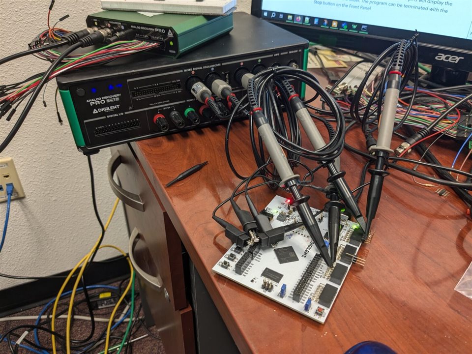
Digilent has recently expanded their test equipment lineup with two powerful new oscilloscopes—the ADP5470 and ADP5490 . These four-channel mixed-signal oscilloscopes offer substantially higher bandwidths and sample rates than any previous Digilent oscilloscope. In this article, we will demonstrate how these enhanced capabilities can be leveraged for advanced FPGA testing applications.
A critical question in FPGA design concerns the maximum toggle frequency of pins—a factor that directly determines data transfer capabilities. This maximum speed is influenced by several variables:
While Pmod connectors are convenient and developer-friendly compared to alternatives like SYZYGY or FMC, they do impose certain speed constraints on signals passing through them.
We developed a custom project that toggles the Pmod I/O pins on an Arty S7 at configurable frequencies. This was accomplished by exposing Clocking Wizard register settings through a command interface connected to a serial port. Using this approach, we could control the serial port from a Python script to consistently configure clock settings while simultaneously recording the resulting clock pulses with the ADP5490.
For readers interested in the details of the FPGA configuration, we covered this topic comprehensively in our earlier post: "VCOs, MMCMs, PLLs, and CMTs – Clocking Resources on FPGA Boards." This current article focuses primarily on the capabilities of the ADP5000 devices.
For proper transmission between devices, digital signals must meet specific voltage thresholds. In the case of 3.3V LVCMOS logic (commonly used on our FPGA boards), a valid rising edge requires a signal transition from below 0.4V to above 2.4V.
These thresholds are documented in Table 8 (SelectIO DC Input and Output Levels) of DS189, Spartan 7 AC/DC Switching Characteristics. It's worth noting that these specifications are defined for DC signals, and their applicability to rapidly toggling pins depends on the board's analog characteristics—precisely what we aimed to test.
Through progressive frequency testing with the oscilloscope, we determined the point at which LVCMOS33 voltage levels could no longer be maintained. WaveForms' cursors feature proved invaluable for quickly assessing whether signals crossed specific thresholds.

We observed output signals with varying phase shifts relative to each other at 10 MHz. The expected shifts were approximately 0 degrees between channels C1 and C2, 45 degrees between C1 and C3, and 90 degrees between C1 and C4. Our measurements confirmed these were reasonably accurate.

At 60 MHz, we noted that slew rates began to significantly impact signal quality, though threshold requirements were still being met. Harmonic frequencies remained present, albeit with reduced impact on square wave edge formation. The ADP5490's high bandwidth allowed us to capture multiple harmonics up to the 7th at 420 MHz.

Signal behavior became particularly interesting at 75 MHz. While the outputs managed to swing past the required thresholds, we observed unexpectedly high amplitude—possibly representing a smoothed-out overshoot condition.

To understand how external components affect signal quality, we compared the JC1 and JA1 outputs at 15 MHz. One output included a series resistor while the other did not, revealing significant differences in signal characteristics. During this testing, we found the Scope to Digital feature especially useful, as it allows interpretation of analog signals in a logic analyzer-style view with adjustable thresholds.
Our previous oscilloscope, the AD3, though extremely useful for many FPGA debugging tasks, lacked sufficient bandwidth for this type of comprehensive testing. The FFT view of clock signals revealed the importance of capturing multiple harmonic frequencies to properly represent square waves as they would be interpreted by driven devices. An oscilloscope must capture frequencies many times higher than the base signal to provide accurate representation.
We must emphasize that all testing was conducted with a specific board and project configuration, with no external circuits beyond the oscilloscope connected to the I/Os. Results will differ substantially once a Pmod is connected to a Pmod port, so actual performance may vary in practical applications.
ADP2230 is a mixed signal oscilloscope (MSO) for professional engineers. It includes analog inputs, analog output, and digital I/O, with deep memory buffers all operating at up to 125 MS/s. Users can receive and generate digital signals to test and analyze data from various devices while simultaneously powering those systems with its robust power supply. The ADP2230 performs the functions of several test and measurement devices and can replace a stack of traditional instruments.
With the included WaveForms software, users can view and capture complex data, perform spectral and network analysis, and quickly retrieve large amounts of data. WaveForms leverages the ADP2230’s deep buffer memory, allowing hundreds of millions of samples to be stored and streamed back to the host computer. WaveForms’ friendly user interface has the feel of traditional benchtop oscilloscopes.

Features:
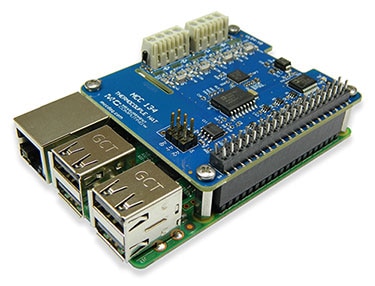
When it comes to temperature measurement, thermocouples stand out as a favored solution owing to their affordability, simplicity, and expansive measurement range. In this article, we'll explain the intricacies of accurate thermocouple measurements, the innovative approach of the Digilent MCC 134 DAQ HAT in tackling these challenges, and how users can optimize their measurements to minimize errors.
Understanding Thermocouples: How They Operate
Thermocouples function by harnessing the Seebeck effect, where thermal gradients generate electrical potential differences. Typically consisting of two wires made of dissimilar metals joined at one end to form a junction, thermocouples produce a voltage in response to temperature variations, facilitating temperature measurement.
Various thermocouple types utilize different metal combinations, catering to distinct temperature ranges. For instance, J type thermocouples, crafted from iron and constantan, excel in measuring temperatures ranging from -210 °C to 1200 °C, while T type thermocouples, employing copper and constantan, are ideal for measurements spanning from -270 °C to 400 °C.
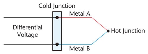
The challenge lies in accurately measuring the temperature difference between the hot (measurement) and cold (reference) junctions, which necessitates precise assessment of the cold junction temperature.
Navigating Thermocouple Measurement Fundamentals
Thermocouples generate a voltage relative to the temperature gradient between the hot and cold junctions. However, determining the absolute temperature of the hot junction requires knowledge of the absolute temperature of the cold junction.
Traditionally, ice baths served as reference points for the cold junction temperature. However, modern measurement devices incorporate sensors to gauge the terminal block's temperature, where thermocouples connect to the measurement apparatus.
Identifying Sources of Thermocouple Errors
Numerous factors contribute to thermocouple measurement errors, including noise, linearity, offset error, the thermocouple itself, and the measurement of the cold junction temperature. While advanced 24-bit measurement devices leverage high-accuracy ADCs and design strategies to minimize errors, thermocouple imperfections remain inevitable.
Addressing Design Challenges of the MCC 134 DAQ HAT
The MCC 134 encounters distinctive design hurdles in ensuring accurate temperature measurements. The MCC 134 faces uncertainties due to temperature gradients induced by external factors like the Raspberry Pi and ambient conditions.
To mitigate inaccuracies, Digilent redesigned the MCC 134 with an enhanced scheme featuring two terminal blocks and three thermistors strategically positioned to track cold junction temperature variations effectively.
Optimizing Thermocouple Measurements with Digilent’s MCC 134
To maximize the accuracy of thermocouple readings using the MCC 134, users should adhere to certain best practices:
In Conclusion
Despite the inherent complexities of thermocouple measurements, the MCC 134 stands as a testament to innovative design and rigorous testing, offering a reliable solution for leveraging standard thermocouples with the Raspberry Pi platform.
Dual mode is a new feature recently unveiled in WaveForms, coinciding with the launch of Analog Discovery 3 . This addition enables users to connect two identical Mixed Signal Oscilloscopes, synchronizing their acquisitions to double the channel count of their acquisition system. This functionality isn't limited to just analog inputs; it extends seamlessly to analog outputs and digital inputs and outputs.
This feature also supports the Analog Discovery Pro 3000-Series, where users can connect two ADP3450s to create an impressive 8-channel scope system. The specific hardware connections required may vary, but for 3000 Series devices, a pair of short coax BNC cables will suffice for the connection.
In this post, we'll guide you through the setup of Dual mode using a pair of AD3 devices and configuring the system to account for clock delay. It's important to note that this feature is supported in version 3.20.1 of WaveForms, the latest release at the time of writing. Additionally, there are some enhancements available in the beta version of WaveForms, 3.20.15, which introduces degree units as a phase adjustment option, and this guide refers to these improvements. You can access beta versions through the Digilent Forum link.
GUIDE:
Hardware Setup
To utilize Dual mode effectively, you must connect the external trigger pins of the two devices. Connect T1 to T1 and T2 to T2. T1 carries a reference clock between the devices, ensuring they use the same clock source, while T2 passes the selected trigger source between them for synchronized acquisitions. Ground connections between the devices should also be established to minimize crosstalk. If you want to further reduce crosstalk, consider using a twisted wire pair for the T1 reference clock signal. Keeping cable lengths as short as possible ensures optimal performance.

Software Setup
Choose the host device, noting that the selection of the first device does not impact functionality.

Click on the "Select + Dual" option and choose the second identical device. Follow the instructions to connect Trigger 1 to Trigger 1, Trigger 2 to Trigger 2, and a ground pin between the two devices.

Open the Scope instrument.

You'll now see a secondary set of analog inputs from the additional device, labeled as Channel 3 (+1±) and Channel 4 (+2±) for a pair of Analog Discovery 3s. Below the screen, you'll find indicators displaying the selected devices, additional device settings, and device status, in that order.

Despite the synchronization of the two devices with a reference clock and trigger line, there might still be some phase differences due to propagation delay. Without adjustments, the same signal sent to both devices may exhibit a delay, typically around 2.5ns.
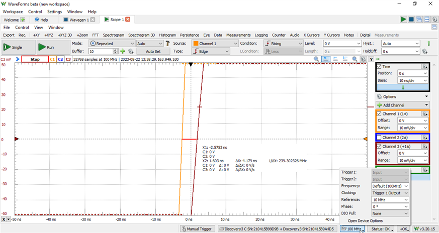
To rectify this, provide a phase adjustment through the "Phase" setting in the Device Options dropdown (the 100 MHz button) at the bottom of the window. This allows you to manually fine-tune the clock for the second device, aligning data sampling with respect to the clock edge. This adjustment compensates for the delay from one device to the other, ensuring data is sampled at approximately the same time.
For precise phase offset selection, employ a shared signal source to test the system. A square wave works well for this purpose, as it facilitates the comparison of rising edges.

Zoom in closely on the trigger point, enabling you to determine the nanoseconds of difference between the primary and secondary device as they cross the same threshold.

Adjust the Phase dropdown in the Device Options until both devices cross the threshold at nearly the same time, fine-tuning until you achieve your desired results.
Keep an eye on the reference clock option, as it allows you to modify the clock's frequency passed over the T1 trigger line. Different frequencies may perform better or worse based on your specific application.
Throughout this process, remember that channel ranges can be adjusted to spread the signal vertically across the plot, making it easier to identify zero crossings.
After some experimentation, you can significantly reduce phase offset. For instance, we managed to reduce it to 247.7 ps out of a 10 ns clock period (100 MHz clock) for our setup, which is ten times better than the default settings.
Conclusion
With these adjustments, you now have access to an oscilloscope system capable of simultaneously sampling four signals, greatly expanding your testing capabilities.


