APPLICATION NOTE
Impact of output capacitor on feedback loop stability of a power supply
ANP117 by Eleazar Falco
1. INTRODUCTION AND THEORETICAL BACKGROUND
A switching power supply requires one or more capacitors across the output voltage rail. Their main purpose is to provide a low-impedance path to filter out the AC current ripple at the converter switching frequency and any high-frequency noise, resulting in a ‘clean’ DC voltage to supply the load. In addition to this, they also act as an energy reservoir. In the case of a sudden change in the load current demand, the output capacitor(s) will provide or absorb energy to or from the load, limiting the output voltage excursions until the control loop reacts and can adjust the amount of energy transferred from the input to the output stage of the converter as necessary. Hence, for a set bandwidth of the feedback control loop, the capacitance and equivalent-series-resistance (ESR) of the output capacitor(s) will dictate the amount of overshoot and undershoot of the output voltage during load transient events. Although these are their two main roles in the converter, the output capacitors also influence the feedback control loop. As they are part of the power stage, their parameters appear on the plant transfer function of the system, shaping its magnitude and phase over frequency. Therefore, once the compensator circuit has been designed for a specific plant characteristic, changes in the output capacitor parameters will in turn affect the phase and gain margins of the control system, with consequences ranging from just a degradation of the transient performance up to full-blown instability in a worst-case scenario. It is therefore important to understand the way such variations affect the stability margins of the system, as well as to verify stability of the control loop whenever changes in the output capacitor(s) are made, as a redesign of the compensator circuit may be required. Against this background, in this application note the role of the main output capacitor parameters on the plant transfer function of a power supply is analyzed, using a buck converter with voltage-mode control (Figure 1) as a reference topology. Additionally, experimental results on a real converter prototype will show the consequences that a change in the output capacitor(s) can have on the stability of the feedback loop and thus, on the converter’s functionality, considering different design scenarios and providing design guidelines as necessary.
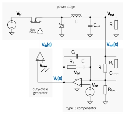
Figure 1: Closed-loop buck converter with voltage-mode control and OP-AMP based type-3 compensator circuit
02. THE OUTPUT CAPACITOR IN THE PLANT TRANSFER FUNCTION
The plant or control-to-output transfer function (abbr. TF) of a switching regulator varies not only with topology and control technique used, but also with component values and operating conditions of the converter. To illustrate the impact of the output capacitor, a VM-CCM buck converter (i.e. buck converter with voltage-mode control and continuous-conduction-mode operation) will be used (Figure 1), but a similar analysis procedure can be followed for other cases. The plant transfer function of the VM-CCM buck converter is widely documented and has the following structure (s-domain):

It can be separated into three different elements: a low-frequency gain (a(s)), a so-called ‘ESR zero’ (b(s)) and a resonant double-pole (c(s)), as follows:
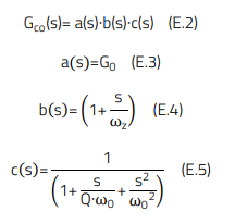
The characteristic of the above transfer function is set by the values of four different variables: G0, ωz, ω0 and Q, which in turn, depend on several converter parameters as below [1]:
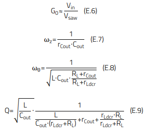
In the expressions above, rCout is the ESR of the output capacitor and rLdcr is the winding resistance of the power inductor. The rest of the parameters are shown in the schematic of figure 1. Note that Vsaw is the amplitude of the voltage sawtooth waveform fed to the comparator to generate the duty-cycle of the control transistor in a voltage-mode converter. The following buck converter specification is considered as an example:

With the above, the calculated parameters of the plant transfer function are (with ω = 2πf): G0 = 21.24 dB, fZ= 18 kHz, f0 = 3.4 kHz, Q = 1.73. The magnitude and phase curves of each of the three elements a(s), b(s) and c(s) are shown separately in Figure 2. It is observed how the low-frequency gain (a(s)) is simply a constant gain, not causing any phase shift over the entire frequency range. The ESR zero (b(s)) provides no gain until fZ, a point where the gain is 3 dB and it keeps increasing at a rate of 20 dB/dec above fZ. Regarding the phase, the ESR zero starts providing phase lead at about one-decade below fZ, reaching 45º at fZ and increasing to 90º at around one-decade above fZ. The resonant double-pole (c(s)) has the typical magnitude and phase curves of the well-known second-order RLC circuit, with its resonance frequency and quality factor determined in previous equations E.8 and E.9. It models the resonance of the power inductor and output capacitor, with lossy elements of the power stage contributing some damping (note that E.8 and E.9 are an approximation, since only the capacitor ESR and inductor DCR were accounted for, but additional lossy elements like a MOSFET Rds(on) were not included). The Bode plot of the plant transfer function of the VM-CCM Buck converter of this example can be built then by adding together the magnitude and phase curves of the three separate factors a(s), b(s) and c(s), and the result is shown in Figure 3.
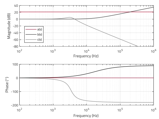
Figure 2: Bode plot of DC-Gain (a(s)), ESR zero (b(s)) and resonant double-pole (c(s)) of VM-CCM buck converter example (MATLAB)
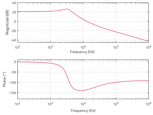
Figure 3: Bode plot of plant TF of VM-CCM buck converter example (MATLAB)
Note how in the low-frequency range below 1 kHz, the plant response is dominated by the constant low-frequency gain with no phase shift. The double-pole at 3.4 kHz comes into action next, causing the magnitude to roll off at a rate of -40 dB/dec while causing a dramatic phase shift heading steeply towards -180°. However, the phase does not reach this value because the ESR zero at 18 kHz counteracts the action of one pole, resulting in a net roll-off of -20 dB/dec and the phase curve heading towards -90° above the ESR zero frequency (fZ). The ESR zero is a common element to all converters with one or more output capacitors, and its frequency position is solely determined by the values of Cout and rCout as in E.7. Once the plant characteristic is known, a common rule-of-thumb is to select the crossover frequency of the open-loop transfer function (at which control loop stability is studied) lower than one-fifth of the switching frequency but also higher than the double-pole frequency. Based on this, the target crossover frequency could then be selected somewhere between 20 kHz and 100 kHz in this example.
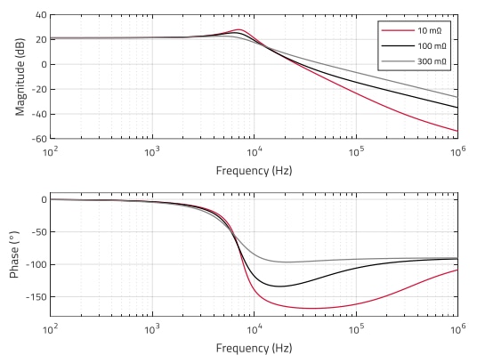
Figure 4: Bode plot of plant TF for fixed Cout=47 µF and varied rCout (MATLAB)
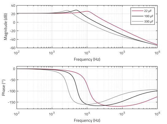
Figure 5: Bode plot of plant TF for fixed rCout=10 mΩ and varied Cout (MATLAB)
Figure 4 and Figure 5 show how different values of Cout and rCout (all of which would be suitable for this example buck converter), influence the plant frequency response. To gain a better insight on the individual effect of Cout and rCout, one of the parameters is kept fixed and the other varied. In Figure 4, Cout is fixed and rCout varied, while in Figure 5, rCout is fixed and Cout varied. Table 1 shows the calculated values of fZ, f0 and Q in each case. It is observed how variations of the ESR mainly affect the ESR zero frequency (fZ), but they do not cause important variations in f0 and Q, whereas variations in the output capacitance notably affect both, the ESR zero as well as the double-pole frequency, while having a negligible effect on the quality factor in this example. This results in important deviations of up to 25 dB in the magnitude curves (Figure 5) and over 70º in the phase curves (Figure 4) within the target frequency range of 20 kHz to 100 kHz.

Table 1: Calculated values of fz, f0 and Q corresponding to Cout and rCout variations considered in figures 4 and 5
How can such variations jeopardize the stability of the converter’s feedback loop? As a brief review, Figure 6 shows the block diagram of the closed-loop VM-CCM buck converter of previous Figure 1, with the transfer functions in the s-domain and considering only AC-signals with the converter’s DC operating point fixed.
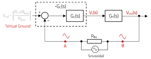
Figure 6: Closed-loop system diagram of VM-CCM buck converter of figure 1 for AC-analysis with injected sinusoidal perturbation
A small-signal sinusoidal perturbation is injected across RINJ (5-10 Ω), and the voltages at points ‘A’ and ‘B’ with reference to DC-GND are observed. If the perturbation in ‘A’, after travelling through the compensator (GC(s)) and plant (GP(s)) arrives at ‘B’ with the same phase and amplitude, then a sustained oscillation has been generated and the system is unstable. In other words, instability results if the product of the compensator (including the inverting action of error amplifier) and plant transfer functions, known as the open-loop transfer function (GOL(s)), provides a total phase lag of 360º or greater to a sinusoidal signal at its crossover frequency (0 dB, Gain=1). Note that the inverting action of the error amplifier around which the compensator circuit is built (equivalent to a 180º phase lag) cannot be separated from GC(s) in the measurement, and then it simply appears as a minus sign for GC(s) in the definition of the plotted open-loop transfer function (E.10).

Based on the above, in the measurements shown in this document, the phase of the open-loop transfer function at the crossover frequency will directly correspond to the ‘phase margin’ (PM). From E.10, it can be observed how the frequency response (Bode plot) of the open-loop transfer function is built by adding the magnitude and phase curves over frequency of the compensator and plant transfer functions. Thus, once the compensator is designed to achieve good stability margins for a specific plant, variations of the plant characteristic caused by changes in the output capacitors will in turn modify the open-loop frequency response, potentially to the extent of causing instability of the control system. In the following section, experimental results on a real VM-CCM Buck converter prototype will show how this may easily happen, considering different design scenarios.
03. EXAMPLE CASE: IMPACT OF ‘BULK’ CAPACITOR
The amount of capacitance required to attenuate the output voltage ripple (at the switching frequency) to sufficiently low values (e.g. 0.5% of Vout) is typically much lower than the amount required for energy storage to meet transient response requirements.
Consider the following basic specification of a VM-CCM buck converter:

To obtain an output voltage ripple amplitude below 0.4% of Vout (i.e. 20 mV in this case), around 26 µF of capacitance is required (considering negligible ESR by using Multilayer Ceramic Capacitors (MLCC)):

The above requirement can be met by paralleling three WCAP-CSGP 885012209028 (10 µF, 25 V, 1210, X7R) capacitors. REDEXPERT curves in Figure 7 show an ESR of around 2 mΩ at 400 kHz with a capacitance drop of only 4.9 % at 5 V bias, resulting in 9.5 µF. Thus, this arrangement would be equivalent to a single capacitor of around 28 µF and 0.7 mΩ, which will be denoted as ‘Co1’ from this point on in the document.
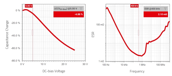
Figure 7: REDEXPERT data for WCAP-CSGP 885012209028
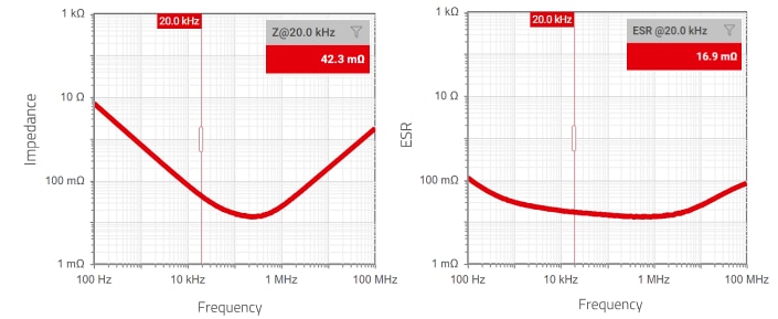
Figure 8: REDEXPERT data for WCAP-HSAH 875585345004
The so-called ‘bulk’ capacitance is added to meet transient specifications. Consider as an example the requirement to keep the output voltage undershoot within 2% of Vout (i.e. 100 mV) for a load current step of 1.5 to 3.5 A. With a 20 kHz feedback loop bandwidth, the formula E.12 (proposed in [2]) gives an estimation of the minimum required ‘bulk’ capacitance, which in this case is around 160 µF. A single WCAP-HSAH 875585345004 hybrid polymer capacitor (220 µF, 16 V, 17 mΩ (at 20 kHz)) can be used to meet this requirement. Its REDEXPERT curves are shown in Figure 8, and it will be referred to as ‘Co2’ from here on.

In Figure 9, the VM-CCM Buck converter prototype is shown with the output capacitors highlighted. The measured plant transfer function in Figure 10 shows a magnitude and phase of -8.5 dB and -146º at 20 kHz. A type-3 compensator providing a gain of 8.5 dB and having a phase of 206º at 20 kHz would result in a 20 kHz crossover frequency and a 60º phase margin. Selecting the following standard component values below (see Figure 1 for schematic reference), a crossover frequency of 21 kHz and a phase margin of 58º are obtained, as shown in Figure 11. Note that the design procedure for the type-3 compensator is beyond the scope of this document, but [3] can be consulted in this regard. Figure 12 shows that the transient response comfortably meets the specification, with an undershoot of around 75 mV.
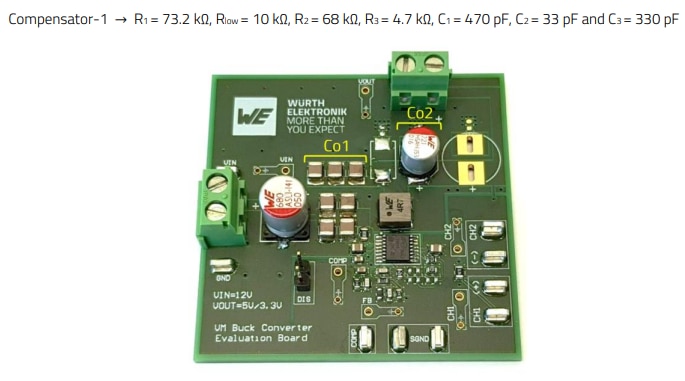
Figure 9: VM-CCM buck converter board with Co1 and Co2 output capacitors
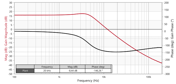
Figure 10: Measured Bode plot of plant TF of VM-CCM buck converter with Co1+Co2 (Bode100)
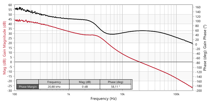
Figure 11: Measured Bode plot of open-loop TF of VM-CCM buck converter with compensator-1 and Co1+Co2 (Bode100)
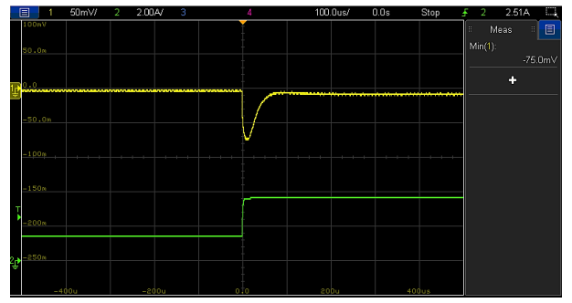
Figure 12: Load transient response (1.5 A to 3.5 A, 1 A/µs) of VM-CCM buck converter with compensator-1 and Co1+Co2 (Vout (l), Iout (l)
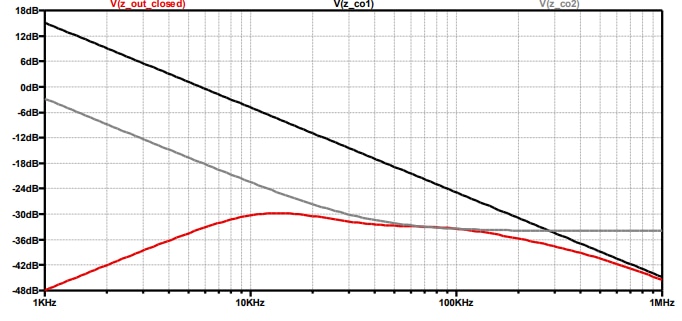
Figure 13: Impedance vs Frequency (closed-loop output impedance (l), Co1 impedance (l), Co2 impedance (l) (LTspice)
Note that the bulk capacitor has almost no influence on the attenuation of the output voltage ripple at the switching frequency of 400 kHz. Figure 13 shows the impedance versus frequency curves of Co1, Co2 as well as the total converter output impedance in closed-loop operation for 2 A output current (LTspice simulation). It is observed how at 400 kHz, the converter output impedance is dominated by Co1 (i.e. 3 x WCAP-CSGP 885012209028 capacitors), while the impedance between 20 kHz and approximately 200 kHz is dominated by Co2 (i.e. WCAP-HSAH 875585345004 capacitor). Below the crossover frequency of 20 kHz, the converter output impedance is set by the control loop to a much lower value than the impedance of the output capacitors. In addition to its main role of keeping the output voltage regulated at the target value despite varying operating conditions, a lower converter output impedance with the subsequent improvement in transient response is one of the advantages of a well-designed feedback loop. Based on this, if the load transient requirements are relaxed at a later stage, or the design is reused for a different specification allowing it, it may be tempting to just remove the bulk capacitor. Figure 14 shows the consequences of doing so while ignoring the compensator. As soon as the converter is powered up, the output voltage oscillates, with an amplitude of around 600 mV and an oscillation frequency of around 80 kHz (nothing to do with the switching frequency ripple at 400 kHz). The controller also operates erratically, randomly enabling and disabling switching. The control loop has become unstable!
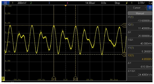
Figure 14: Unstable operation of the VM-CCM buck converter with compensator-1 and without Co2 (Vout (l))
Under such operating conditions, any efforts to directly measure the frequency response would be in vain. However, alternative approaches can be used to confirm that such behavior is effectively caused by an unstable control loop. One is by using an analytical model as in previous section 2 of this document, while other options are via SPICE simulation or even (indirectly) experimentally. This last approach consists of generating the equivalent open-loop frequency response by adding the measured frequency response curves of the compensator-1 and of the plant without Co2, both measured with a stable loop (i.e. compensator-1 measured with Co2 added, and the plant measured with Co2 removed but using compensator-2 as shown later). The results of this experimental approach are shown in Figure 15, where a negative phase margin of -15º confirms instability. Note how the output voltage oscillation frequency of 80 kHz observed in Figure 14 is very close to the open-loop crossover frequency of 89 kHz in Figure 15. For further insight, the measured Bode plots of the plant transfer function with and without the bulk capacitor are compared in Figure 16. The two curves at the top correspond to the magnitude (left axis reference), and the two curves at the bottom to the phase (right axis reference). After removing the bulk capacitor, the double-pole frequency increases from 5 kHz to 14 kHz and so does its quality factor, from 1.2 to 2.5. The ESR zero moves from around 50 kHz up to 8.2 MHz, ‘disappearing’ from the response, and with it the beneficial phase lead contributed in the range between 20 kHz and 100 kHz. In this frequency range, these variations have the combined effect of an increase in gain and additional phase lag. Consequently, with compensator-1, the resulting crossover frequency moves higher to around 80-100 kHz caused by the double-pole frequency shift, an area where the phase lead provided by the compensator is lower (see Figure 15) and the plant phase lag higher (due to the absence of the ESR zero). An unfavorable combination.
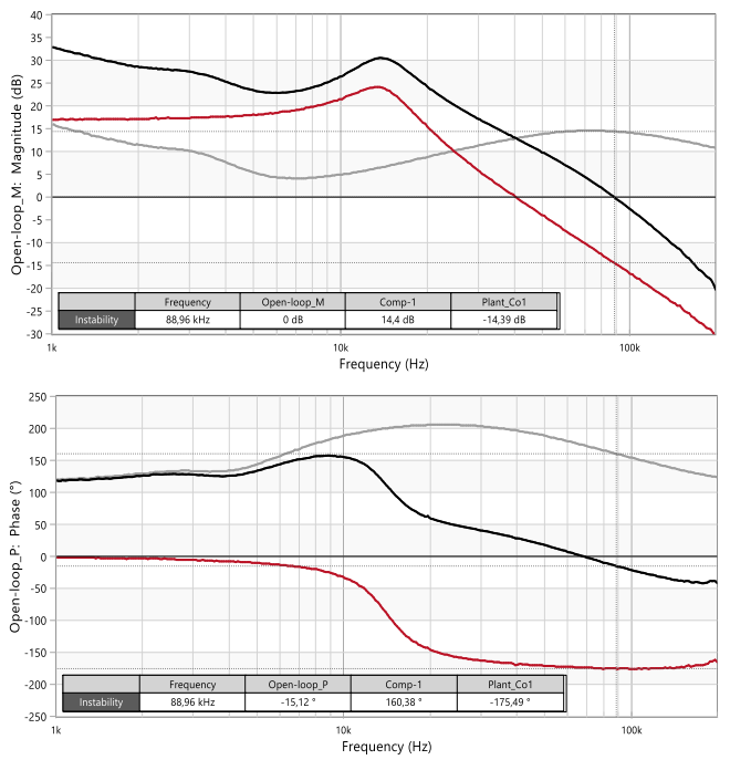
Figure 15: Bode plots of measured plant TF (with Co1-only) (l), measured compensator-1 (l) and generated open-loop TF (l) (Bode100)
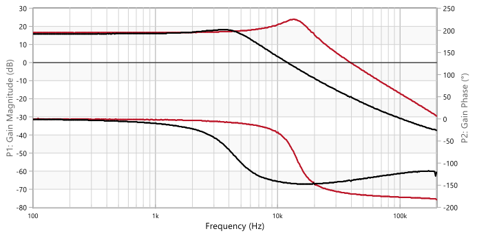
Figure 16: Comparison of measured plant TF: Co1 only (l), Co1+Co2 (l). Magnitude (dB) (top curves). Phase (º) (bottom curves) (Bode100)
A redesign of the compensator is necessary to bring the converter back to stability without the bulk capacitor. Considering the original specification of a 20 kHz crossover frequency and a phase margin of 60º, the new compensator components are recalculated and the following standard values selected:

The measured open-loop frequency response in figure 17 shows a crossover frequency of 21 kHz, a phase margin of 59.9º and a gain margin of nearly 25 dB. The well-behaved transient response in figure 18 further confirms stability, albeit suffering from a much higher undershoot amplitude of 0.5 V due to lower energy storage capability with the absence of the bulk capacitor, as expected. When it comes to design robustness, one may feel uneasy that the crossover frequency is now rather close to the double-pole frequency. Just about 8 dB of attenuation will be enough to make the double-pole peaking dive below the 0 dB line, causing a sudden reduction of the crossover frequency below 1 kHz, with the loop not having enough gain to counteract the double-pole resonance.
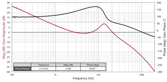
Figure 17: Measured Bode plot of open-loop TF of VM-CCM buck converter with compensator-2 and Co1 only (Bode100)
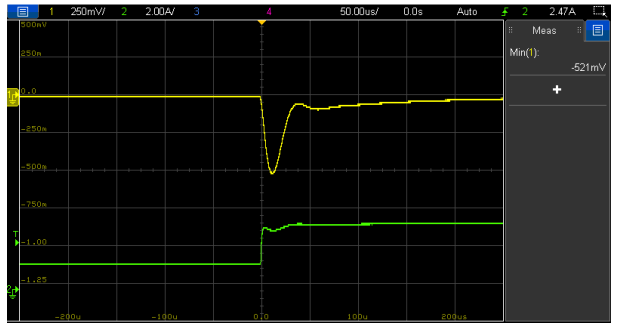
Figure 18: Load transient response (1.5 A to 3.5 A, 1 A/µs) of VM-CCM buck converter with compensator-2 and Co1 only (Vout (l), Iout (l))
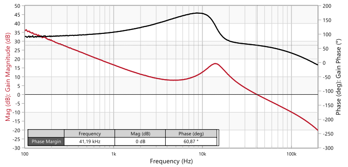
Figure 19: Measured Bode plot of open-loop TF of VM-CCM buck converter with compensator-3 and Co1 only (Bode100)
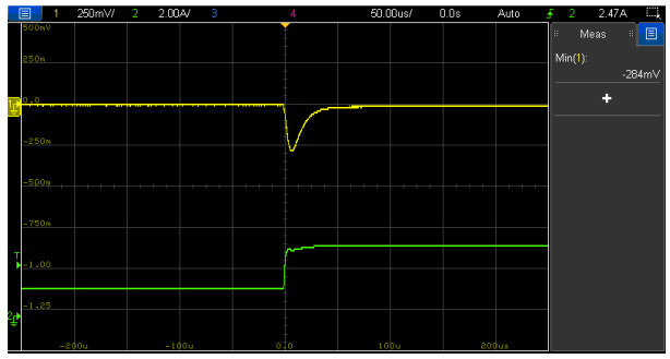
Figure 20: Load transient response (1.5 A to 3.5 A, 1 A/µs) of VM-CCM buck converter with compensator-3 and Co1 only (Vout (l), Iout (l))
Peace of mind can be restored by redesigning the compensator for a higher crossover frequency of 40 kHz, without added cost and with the only drawback of an increased susceptibility to noise of the loop at higher frequencies. The compensator component values are as follows:

Figure 19 shows the more robust design, now requiring over 18 dB to bring the peaking below the 0 dB line. Observe how increasing the crossover frequency has also brought another advantage, as it improved the transient response reducing the undershoot amplitude to 0.28 V thanks to the higher bandwidth and faster reaction time of the control loop (Figure 20). At this point, one may wonder what would happen if the bulk capacitor (Co2) is added without a compensator redesign… Measurement results in Figure 21 and Figure 22 show how the system is much more forgiving in this case, with the phase margin falling slightly to 49º and a well-behaved transient response. A compensator redesign would be recommended for better transient performance and increased ruggedness of the control-loop but it is by no means essential for stability considerations.
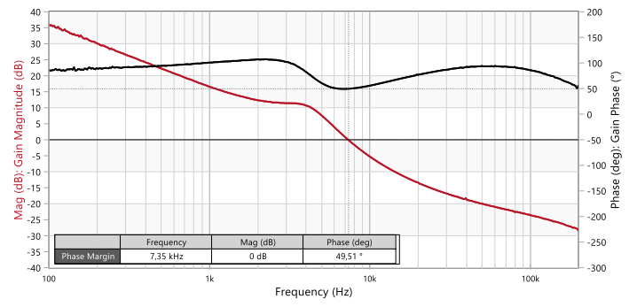
Figure 21: Measured Bode plot of open-loop TF of VM-CCM buck converter with compensator-3 and Co1+Co2 (Bode100)
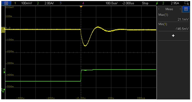
Figure 22: Load transient response (1.5 A to 3.5 A, 1 A/µs) of VM-CCM buck converter with compensator-3 and Co1+Co2 (Vout (l), Iout (l))
04. EXAMPLE CASE: IMPACT OF ESR
In the previous case, there was a considerable variation of both the capacitance and ESR values with the addition and removal of the bulk capacitor (Co2). However, there are situations in a design cycle where the output capacitor must simply be replaced by an equivalent part (i.e. with the same capacitance and similar (or lower) ESR). This could be, for example, due to stock availability issues, change of assembly method (e.g. through-hole (THT) to surface-mount (SMT)), new mechanical constraints or simply for cost reduction efforts. Could a moderate ESR change alone be sufficient to compromise the stability of the converter’s feedback loop? Let us consider the following basic specification of a Buck converter:

Note how the main difference compared to the base specification of the previous example is the lower output voltage (3.3 V instead of 5 V). Therefore, the same WCAP-CSGP MLCC capacitors can be used (Co1) to deal with the output voltage ripple requirement, but now together with the ‘bulk’ electrolytic capacitor WCAP-ATLI 860080474010 (220 µF, 25 V, 70 mΩ (at 30 kHz), THT, (Height-11.5mm, Diameter-8mm)), which will be referred to as ‘Co3’ in the document.
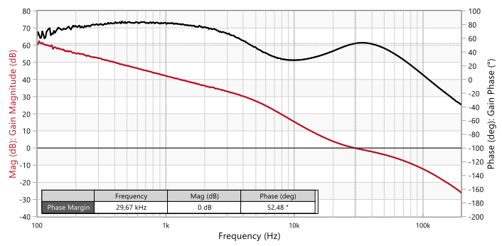
Figure 23: Measured Bode plot of open-loop TF of VM-CCM buck converter with compensator-4 and Co1+Co3 (Bode100)
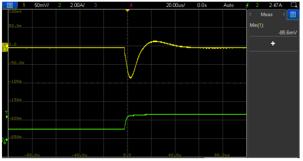
Figure 24: Load transient response (1.2 A to 2.7 A, 1 A/µs) of VM-CCM buck converter with compensator-4 and Co1+Co3 (Vout (l), Iout (l))
With the following compensator component values below, a crossover frequency of 30 kHz with a phase margin of 52° is obtained (Figure 23). The response to a load current step from 1.2 to 2.7 A is shown in Figure 24.

Let us consider that on a later revision of the design, there is a constraint for a maximum height of 4 mm and with all components being surface mount (SMT). In such case, the H-chip polymer capacitor WCAP-PHGP 875015119006 (220 µF, 6.3 V, 5 mΩ (at 30 kHz), SMT, Height-1.9mm) would be a good fit and will be referred to as ‘Co4’. This low-profile capacitor has the same capacitance but a lower ESR than Co3, which is an advantage as it could replace not only Co3, but also the three MLCC capacitors (Co1) altogether, while keeping the switching frequency ripple within the specification and further improving the transient response. However, Co1 will still be left in place for the sake of an accurate comparison against Co3. REDEXPERT data for both capacitors, Co3 and Co4, is shown in Figure 25 left and right, respectively. Upon replacing Co3 by Co4 with the fixed compensator-4, the control loop (12 V to 3.3 V, 2.5 A) is on the brink of instability with a measured phase margin below 3° and a crossover frequency around 18 kHz (Figure 26).
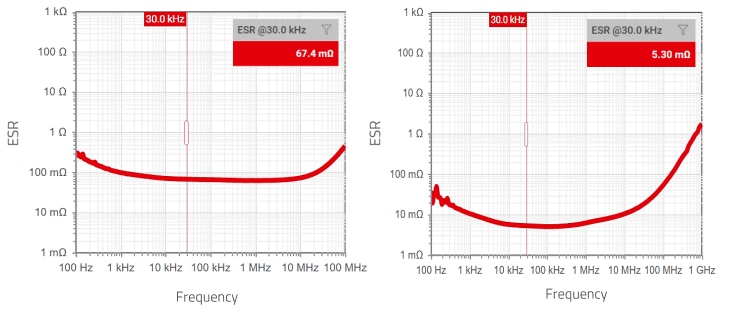
Figure 25: REDEXPERT ESR data for Co3 (WCAP-ATLI 860080474010) (left) and for Co4 (WCAP-PHGP 875015119006) (right)
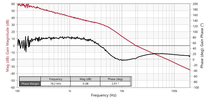
Figure 26: Measured Bode plot of open-loop TF of VM-CCM buck converter with compensator-4 and Co1+Co4 (Bode100)
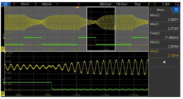
Figure 27: Load transient response for small step (2.15 A to 2.3 A) of VM-CCM buck converter with compensator-4 and Co1+Co4 (Vout (l), Iout (l)
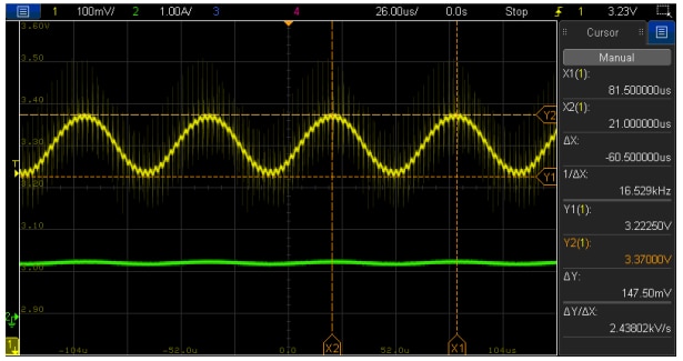
Figure 28: Permanent oscillation of VM-CCM buck converter (12 V to 3.3 V, 1.3 A) with compensator-4 and Co1+Co4 (Vout (l), Iout (l))
Despite the still marginal ‘theoretical’ stability, the converter is unusable in these conditions. In fact, small changes in converter operating conditions (e.g. input voltage, load current) and standard component parameter variations (e.g. tolerance, temperature dependence, etc.) will suffice to also push the converter into theoretical instability. In Figure 27, measurement results for a small load transient step between 2.3 A and 2.15 A are shown, where it is observed how the step-down transient to 2.1 A causes a permanent oscillation at 17.5 kHz, whereas for the step-up transient to 2.3 A oscillations are long-lived but decay, as the system still has a small phase margin above a load current of around 2.2 A. After powering up the converter at a lower output current of 1.3 A (RL=2.5 Ω), a permanent oscillation of 16.5 kHz and 170 mV amplitude appears on top of the DC output voltage of 3.3 V (Figure 28). If a load transient is applied under these conditions, the converter goes into erratic operation, randomly enabling and disabling switching. Note how in the results of Figure 27 and Figure 28, the oscillation frequency is very close to the 18 kHz crossover frequency measured in previous Figure 26, confirming control loop instability. How did the plant characteristic change to cause this scenario? Figure 29 shows the comparison of the plant frequency response for Co1+Co3 (black curves) and for Co1+Co4 (red curves). The two top curves correspond to the magnitude (dB), while the two bottom curves to the phase (deg). The well-damped double-pole frequency remains practically unchanged, as expected with just a moderate change in ESR. The main difference is the shift of the ESR zero frequency. With Co3, this is at around 9 kHz while it moves to nearly 100 kHz with Co4, causing a steeper roll-off of the magnitude curve, which results in a lower gain and higher phase lag in the frequency range from 10 kHz to 50 kHz. As a result, the lower gain shifts the crossover frequency down from 30 kHz to 18 kHz, an area where the phase difference between the two plant responses is maximum (around 40º) and the compensator phase lead lower. Again, an unfavorable combination.
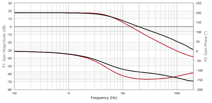
Figure 29: Comparison of measured plant TF: Co1+Co4 (l), Co1+Co3 (l). Magnitude (dB) (top curves). Phase (º) (bottom curves) (Bode100)
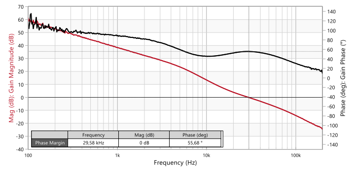
Figure 30: Measured Bode plot of open-loop TF of VM-CCM buck converter with compensator-5 and Co1+Co4 (Bode100)
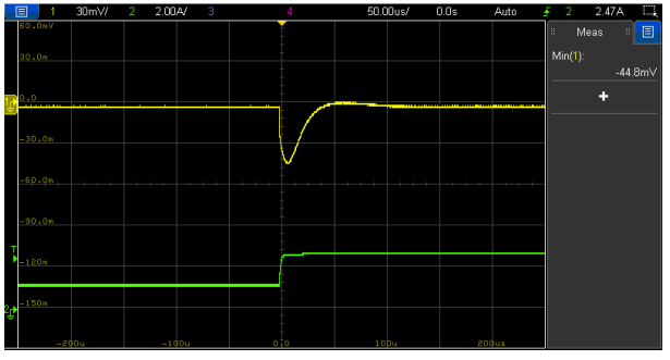
Figure 31: Load transient response (1.2 A to 2.7 A,1 A/µs) of VM-CCM buck converter with compensator-5 and Co1+Co4 (Vout (l), Iout (l))
A compensator redesign is therefore necessary in this case. With the following compensator component values below, a crossover frequency of 29.5 kHz with a phase margin of 55° is obtained (Figure 30):

In Figure 31, an improved transient response is observed with the undershoot reducing from 85 mV down to 45 mV compared to the result with Co3, mainly thanks to the lower ESR of the H-chip polymer capacitor (Co4). What would happen if Co4 is replaced by Co3 with this new compensator? Figure 32 shows a higher crossover frequency of 82 kHz and a phase margin of 33º. Referring back to Figure 29, the higher crossover frequency is explained by the higher gain of the plant transfer function with Co3, while the reduction of the phase margin is mainly due to the lower phase lead provided by the compensator in this range, since the plant transfer functions of both Co3 and Co4 cause a similar phase lag between 70 and 100 kHz. Similar to the previous example, a higher ESR is more forgiving when it comes to stability of the control system also in this case. However, a compensator redesign would be highly recommended since 30º is a rather low nominal phase margin. For reference, Figure 33 shows the VM-CCM Buck converter board with Co1, Co3 and Co4 capacitors.
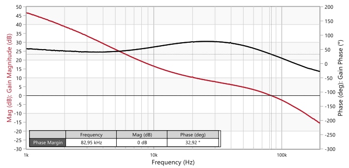
Figure 32: Measured Bode plot of open-loop TF of VM-CCM buck converter with compensator-5 and Co1+Co3 (Bode100)
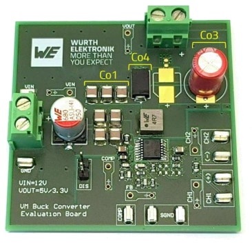
Figure 33: VM-CCM buck converter board with Co1, Co3 and Co4 output capacitors
In this example design case, the impact of an ESR variation from around 5 to 70 mΩ was studied. Although this may seem a large variation, it is in fact a rather moderate change considering the actual spread of ESR values which can be found in practice. REDEXPERT results in Figure 34 show an ESR range from around 70 mΩ to slightly over 1 Ω at 30 kHz, considering four 100 µF capacitors within the same series (WCAP-ATLL), with varying size and voltage ratings. Even for similar 220 µF capacitors as in these two example cases, with a fixed voltage rating of 25 V and considering different WCAP series, the ESR values spread over a range from 7 mΩ up to around 300 mΩ, as shown in Figure 35. Without any fixed parameters, ESR differences would easily span a range of several orders of magnitude, from a few tens of µΩ to several Ohms. Therefore, it is recommended to verify feedback loop stability margins even when the output capacitor is replaced by an equivalent part with the same capacitance, especially in cases involving more than a two-fold change of the ESR.
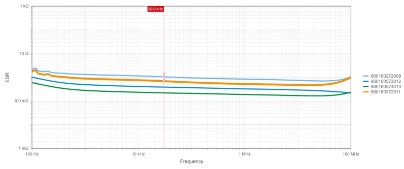
Figure 34: REDEXPERT ESR vs Frequency curves for different 100 µF WCAP-ATLL capacitors
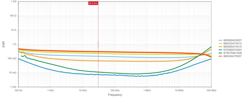
Figure 35: REDEXPERT ESR vs Frequency curves for 220 µF, 25 V capacitors from different WCAP series
05. STABILITY FOR ANY OUTPUT CAPACITOR WITHOUT COMPENSATOR REDESIGN?
Although a compensator specifically designed and tailored to a specific plant will provide the best performance, there may be cases where designing a compensator which can ensure a stable control loop despite wide variations of the plant characteristic may be the preferred solution. Amongst others, this would allow to replace components like the power inductor or output capacitor at a later stage without a concern for stability. Would that be possible? In Figure 36, the measured plant frequency response of the different output capacitor combinations considered so far in the document is shown. These are: Co1-only, Co1+Co2 and Co1+Co3 (note that Co4 has similar ESR than Co2 and it is therefore not included). It can be observed how the variations of capacitance and ESR values do not affect the plant response in the lowfrequency range below around 1 kHz, where the plant characteristic is dominated by the constant low-frequency gain with little to no phase lag added. Therefore, if the crossover frequency is selected at or below 1 kHz in this case, an integrator configuration, also known as type-1 compensator (Figure 37) could be used, consisting in a simple origin pole. Its integrating action eliminates the static error (i.e. the output voltage closely following the reference), while producing a total phase lag of 270º (i.e. 180º from the inverting action of the error amplifier and 90º due to the capacitor C1). With this, a phase margin of 90º would be obtained, independent of the output capacitor.
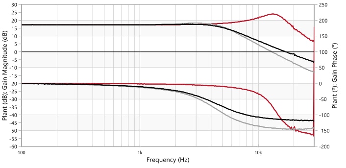
Figure 36: Measured Bode plot of plant TF of VM-CCM buck (12 V to 5 V, 2 A) for Co1-only (l), Co1+Co2 (l) and Co1+Co3 (l)
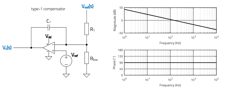
Figure 37: Type-1 compensator circuit and its frequency response in this design (compensator-6)
For this compensator, C1 is calculated to set the target crossover frequency of the open-loop transfer function (fCO), as follows:

With R1 = 73.2 kΩ and G0 = 6.3 (i.e. 16 dB), then C1 = 15 nF (compensator-6) will set a crossover frequency of around 1 kHz. Figure 38 shows measurement results of the open-loop transfer function for each of the output capacitor combinations previously mentioned. In all cases, a crossover frequency around 1.1 kHz with a phase margin over 80º and a gain margin no lower than 10 dB are observed, even with a large variation of capacitance and ESR values as in the case of Co1-only. Figure 39, Figure 40 and Figure 41 show the transient response for each case. Despite a lower load current step of 1 A, a more sluggish response with higher undershoot and a longer settling time is observed compared to previous results. Despite high stability margins, a rather underdamped oscillatory response is observed for the ‘Co1-only’ case. The oscillation frequency is 13.5 kHz, which corresponds to the double-pole resonance frequency of its corresponding plant response (see previous Figure 36). This should not come as a surprise, since with a crossover frequency lower than the double-pole frequency, the control loop does not have enough gain to correct for high quality factors of the resonant double-pole. This is one of the trade-offs of this solution, and it is important to understand that in the case of a very high quality factor, the peaking of the magnitude curve could cross the 0 dB line again, possibly making the loop unstable altogether. Aside from this, this approach can keep the control loop theoretically stable with a fairly wide range of output capacitors, albeit at the expense of degraded transient performance.
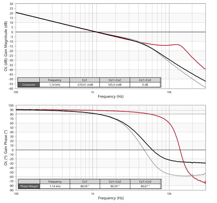
Figure 38: Measured Bode plot of open-loop TF of VM-CCM buck (12 V to 5 V, 2 A) with compensator-6 and for: Co1 (l), Co1+Co2 (l) and Co1+Co3 (l)
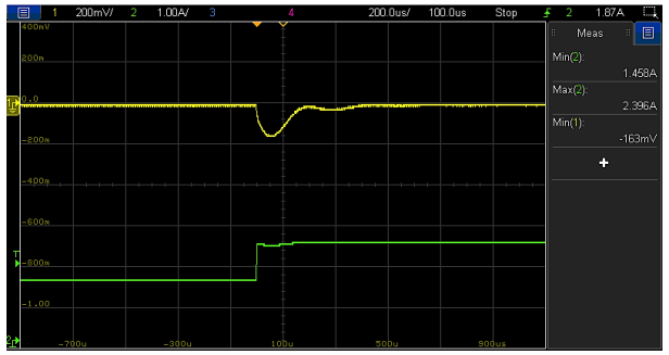
Figure 39: Load transient response (1.4 A to 2.4 A,1 A/µs) of VM-CCM buck converter with compensator-6 and Co1+Co3 (Vout (l), Iout (l))
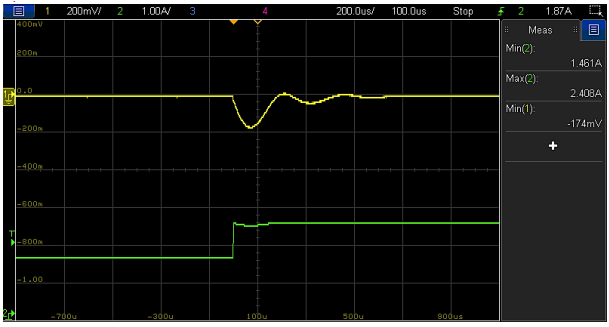
Figure 40: Load transient response (1.4 A to 2.4 A, 1 A/µs) of VM-CCM buck converter with compensator-6 and Co1+Co2 (Vout (l), Iout (l))
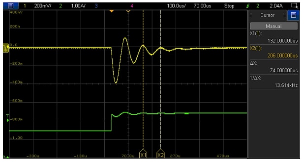
Figure 41: Load transient response (1.4 A to 2.4 A, 1 A/µs) of VM-CCM buck converter with compensator-6 and Co1 only (Vout (l), Iout (l))
06. SUMMARY AND CONCLUSION
In a switching power supply, the output capacitors are typically selected based on voltage ripple and transient response requirements. However, they also affect the feedback control loop as they shape the plant transfer function of the converter. As the compensator circuit is designed for a specific plant characteristic, changes in output capacitor parameters may cause not only a reduction of stability margins, but also full-blown instability of the feedback control loop. There are different scenarios during a design cycle involving a change in the output capacitors of the power supply, like for example, the removal of a ‘bulk’ capacitor (resulting in an important reduction in capacitance and ESR), and the replacement of the output capacitor by an equivalent part (with same capacitance but lower ESR). Both cases have been considered in this document with a VM-CCM buck converter design example. Despite moderate parameter variations, it was observed how the control-loop went from stable operation with comfortable stability margins to instability after the change of the output capacitors, requiring in both cases a compensator redesign to restore stable operation. Although a change involving an increase of capacitance and/or ESR was found to be more forgiving, stability margins did also suffer. Therefore, stability should not be assumed and should always be verified whenever a change in output capacitor(s) is implemented, especially when involving more than a two-fold variation in capacitance and/or ESR. For the specific case of a VM-CCM buck converter as covered here, if the resonance of the power inductor and output capacitor(s) is well damped, the crossover frequency could be shifted lower in the range where the plant characteristic is dominated by the low-frequency gain. This would ensure stability of the feedback loop for a wide range of output capacitors without requiring a compensator redesign, albeit at the expense of a degraded transient performance.
A Appendix
A.1 Frequency response measurement setup
Figure 42 shows the test setup used to obtain the Bode plots shown in the document (based on previous Figure 6). A vector network analyzer (Bode100) was used with the sinusoidal signals injected via an isolation transformer (B-WIT-100
). Note that a resistive load should be used and electronic loads better avoided for this test, as they may interfere with the measurement.
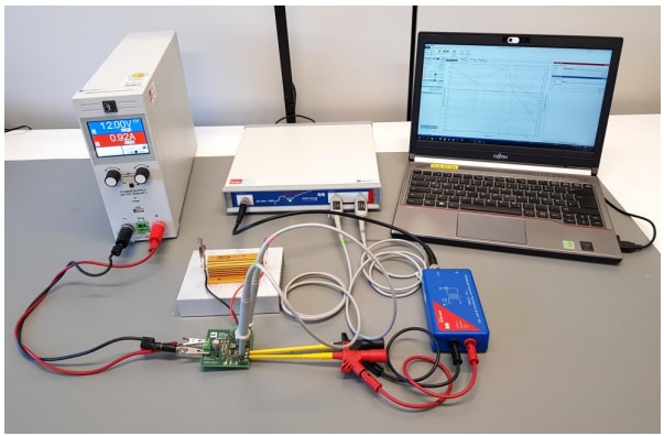
Figure 42: Measurement setup for frequency response
A.2 Load transient response measurement setup
Figure 43 shows the test setup used to obtain the load transient results shown in the document. Resistive loads were used with a pass-transistor control board to create the fast load transient steps.
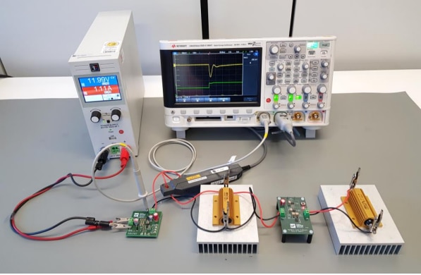
Figure 43: Measurement setup for load transient response
A.3 References
[1] C. Basso, Switch-Mode Power Supplies: SPICE Simulations and Practical Designs, 2nd Ed., McGraw-Hill Professional, 2014
[2] C. Basso, ‘Linking the crossover frequency and the output voltage undershoot’ (www.powersimtof.com/Spice.htm)
[3] C. Basso, Designing Control Loops for Linear and Switching Power Supplies: A Tutorial Guide, Artech House, 2012
IMPORTANT NOTICE
The Application Note is based on our knowledge and experience of typical requirements concerning these areas. It serves as general guidance and should not be construed as a commitment for the suitability for customer applications by Würth Elektronik eiSos GmbH & Co. KG. The information in the Application Note is subject to change without notice. This document and parts thereof must not be reproduced or copied without written permission, and contents thereof must not be imparted to a third party nor be used for any unauthorized purpose. Würth Elektronik eiSos GmbH & Co. KG and its subsidiaries and affiliates (WE) are not liable for application assistance of any kind. Customers may use WE’s assistance and product recommendations for their applications and design. The responsibility for the applicability and use of WE Products in a particular customer design is always solely within the authority of the customer. Due to this fact it is up to the customer to evaluate and investigate, where appropriate, and decide whether the device with the specific product characteristics described in the product specification is valid and suitable for the respective customer application or not. The technical specifications are stated in the current data sheet of the products. Therefore the customers shall use the data sheets and are cautioned to verify that data sheets are current. The current data sheets can be downloaded at www.we-online.com. Customers shall strictly observe any product-specific notes, cautions and warnings. WE reserves the right to make corrections, modifications, enhancements, improvements, and other changes to its products and services. WE DOES NOT WARRANT OR REPRESENT THAT ANY LICENSE, EITHER EXPRESS OR IMPLIED, IS GRANTED UNDER ANY PATENT RIGHT, COPYRIGHT, MASK WORK RIGHT, OR OTHER INTELLECTUAL PROPERTY RIGHT RELATING TO ANY COMBINATION, MACHINE, OR PROCESS IN WHICH WE PRODUCTS OR SERVICES ARE USED. INFORMATION PUBLISHED BY WE REGARDING THIRD-PARTY PRODUCTS OR SERVICES DOES NOT CONSTITUTE A LICENSE FROM WE TO USE SUCH PRODUCTS OR SERVICES OR A WARRANTY OR ENDORSEMENT THEREOF. WE products are not authorized for use in safety-critical applications, or where a failure of the product is reasonably expected to cause severe personal injury or death. Moreover, WE products are neither designed nor intended for use in areas such as military, aerospace, aviation, nuclear control, submarine, transportation (automotive control, train control, ship control), transportation signal, disaster prevention, medical, public information network etc. Customers shall inform WE about the intent of such usage before design-in stage. In certain customer applications requiring a very high level of safety and in which the malfunction or failure of an electronic component could endanger human life or health, customers must ensure that they have all necessary expertise in the safety and regulatory ramifications of their applications. Customers acknowledge and agree that they are solely responsible for all legal, regulatory and safety-related requirements concerning their products and any use of WE products in such safety-critical applications, notwithstanding any applicationsrelated information or support that may be provided by WE. CUSTOMERS SHALL INDEMNIFY WE AGAINST ANY DAMAGES ARISING OUT OF THE USE OF WE PRODUCTS IN SUCH SAFETYCRITICAL APPLICATION.
DIRECT LINK
ANP117 | Impact of output capacitor on feedback loop stability of a power supply
USEFUL LINKS:
Application Notes : https://we-online.com/en/support/knowledge/application-notes
Services: https://we-online.com/en/products/components/service
Contact : https://we-online.com/en/support/contact
CONTACT INFORMATION
Würth Elektronik eiSos GmbH & Co. KG
Max-Eyth-Str. 1, 74638 Waldenburg, Germany
Tel.: +49 (0) 7942 / 945 – 0
Email: appnotes@we-online.de

.png-1440x400x2.png?sv=2016-05-31&sr=b&sig=XudNdwAFDMRQ1fbga3u%2F4DDb7yzNxF7Bf7FWQYQ%2Bda8%3D&se=2026-04-04T23%3A59%3A59Z&sp=r&_=+kQN76cMzUdKXzs+JYKU4g==)