


Application Note
ANP146 | Theoretical Insights and Practical Applications of the WE-CMDC Series Common Mode Chokes
ANP146 by Dr.-Ing. Heinz Zenkner
1. INTRODUCTION
Common mode chokes (CMCs) are widely used to filter out interference components in electronic circuits. These components specifically target noise signals that appear on line pairs with the same amplitude and phase relative to the reference ground. Accurately modeling the behavior of CMCs is crucial for understanding the component in detail. Furthermore, the transfer of the model and its functional simulation into practice must be understood in order to achieve their effective integration into complex systems and for enabling targeted optimization of their filtering performance. This paper presents a simulation of a common mode choke and compares the results with real-world measurements. Additionally, it explores unconventional applications of CMCs, expanding the potential use cases for these components. Notably, the parasitic properties of CMCs are also leveraged as functional elements within certain circuit designs, demonstrating their versatility beyond traditional applications.
2. LTSPICE SIMULATION OF CMCs
CMCs are passive components that generate a high impedance in a certain frequency range to reduce the propagation of unwanted signals (typically electromagnetic noise). The structure of the CMC is the same as that of a wound coil: There is a core of ferromagnetic material, and several wires wound on this core. Figure 1 shows the basic structure of a CMC. The CMCs in detail differ not only in the number of turns and the design, but also in the type of core chosen for specific applications. The core material has a poor quality factor above a few tens of MHz, i.e. it is chosen so that it causes as many losses as possible above a certain frequency range; Iron powder cores are active at low frequencies (fC < 3 MHz, typically below 500 kHz), Manganese-Zinc cores work at higher frequencies (between 200 kHz and 30 MHz), and Nickel-Zinc cores are suitable for even higher frequencies (fC > 10 MHz up to several hundred MHz). Bifilar and sectional winding styles impact the performance and behavior of the choke, particularly in electromagnetic compatibility (EMC) and filtering applications.
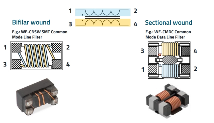
Figure 1: Basic structure of a CMC. Left hand side: Bifilar winding style, right hand side: Sectional winding style.
In bifilar winding style, two wires (or more) are wound together closely in parallel on the core (left in Figure 1). Bifilar winding provides excellent magnetic coupling between the windings, which enhances the inductance for common-mode currents. Since the wires are wound together, the design is compact and easy to manufacture. The chokes are effective at blocking high-frequency common-mode noise due to the high coupling and resulting inductance. The close coupling cancels the inductance for differential-mode currents, making it less effective at suppressing differential-mode noise. The proximity of the wires increases interwinding capacitance, which can degrade performance at very high frequencies. In sectional winding style (inductor on the right in Figure 1), the windings are separated into different sections on the core. The wires are wound in physically distinct layers or areas, with spacing between them. The separation of windings lowers interwinding capacitance, improving high-frequency performance. Due to less coupling, the choke provides some differential-mode inductance, aiding in suppressing differential-mode noise. The separation can improve heat dissipation. The inductance for common-mode currents is lower compared to bifilar winding. Sectional winding often results in a larger choke, as the windings are spaced out.
CMCs are combined with capacitors to form complex filter circuits to achieve the highest possible insertion loss and thus filter effect. How these circuits work, where the weaknesses and strengths lie and how impedance ratios of the system have to be taken into account can best be explained with a simulation, which was carried out below with LTspice.
2.1 Simulation of the CMC WE-CMDC as part of a filter
In the following analysis using LTspice, the common mode attenuation and the differential mode attenuation are considered separately. The simulation circuit diagram without choke is shown in Figure 2. The common mode interference signal source (CM) generates a signal with an amplitude of 1 V at a frequency of 5 MHz and is coupled into the circuit via two 200 pF capacitors. The useful signal, the differential mode signal (DM), has an AC voltage amplitude of 1 V at a frequency of 500 kHz and an additional DC voltage amplitude of 10 V, for better visualization in the diagram. Both signals can be viewed at the load R3.
To illustrate how the CM choke acts as part of a filter, the component is considered under different functional states in the time and frequency domain.
The measurements in Figure 3 clearly show that when a single choke (L3) with capacitor (C10) is implemented in one of the two paths, there is no attenuation of the signals with respect to ground, which is the CM signal.
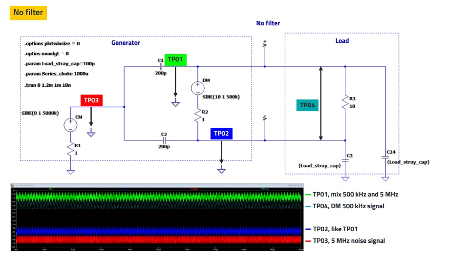
Figure 2: Circuit diagram without CM choke. TP01 to TP04 show the respective voltages
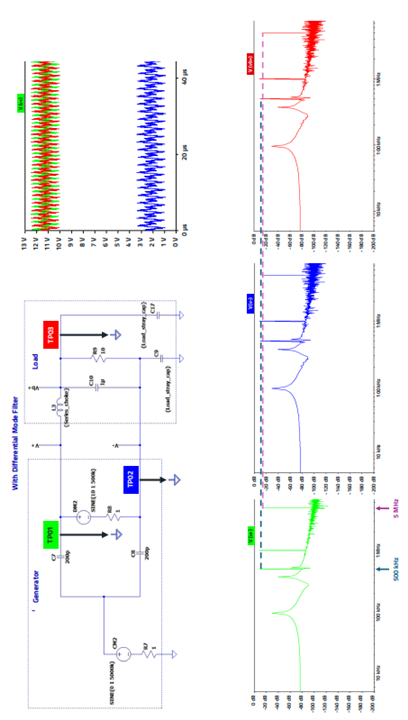
Figure 3: Visualization of the amplitudes of the measuring points in the time and frequency domain (L3 = 1000 µH, C9/C17 = 100 pF).
Both the time and frequency domains are shown; in the time domain, the offset of the signals in the choke path due to the DC voltage can be seen. The time domain shows the 500 kHz and 5 MHz spectral lines at the various measurement points. The levels at the measuring points do not differ in amplitude.
Figure 4 shows that only the differential signal is strongly attenuated in its AC voltage amplitude (TP01, blue).
As the CM interference signal is on both paths, i.e. V+ and V-, both paths must also be provided with filter components to attenuate the interference in relation to ground. For this reason, an unbalanced filter (e.g. LC low-pass filter) cannot be used here. Two chokes were used in the setup in Figure 5.
There is a clear attenuation of the interference signal by approx. 30 dB, but the useful signal is also strongly attenuated, as the diagram clearly shows in the time domain. Therefore, the concept of current compensation must be introduced in order not to attenuate the DM signal.
In a common-mode choke, the windings act in such a way that the magnetic fields of the currents in differential mode cancel each other out, while they add up in common mode. The current in differential mode flows through the windings in opposite directions, whereby the magnetic fields generated ideally compensate each other completely. As a result, the inductance for differential currents approaches zero, which does not attenuate the normal signal flow. With common mode currents, the currents flow in the same direction through both windings, whereby the magnetic fields are added together, and a high inductance is created.
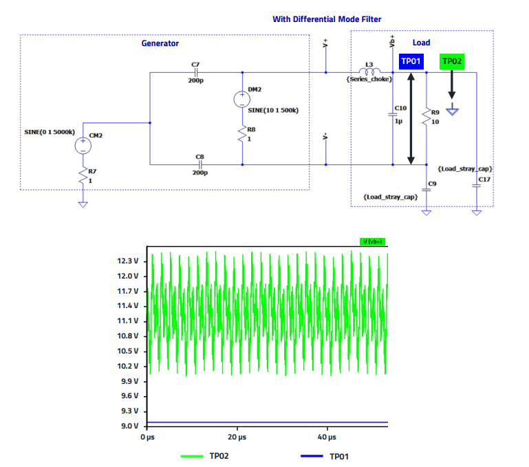
Figure 4: Visualization of the amplitudes of the measuring points behind the filter in the time domain, (L3 = 1000 µH, C9/C17 = 100 pF).
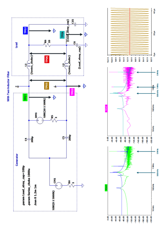
Figure 5: Filter with two chokes (L1, L2), Both DM and CM signals are attenuated. TP05/TP06 show the differential-mode attenuation (signal at 500 kHz), TP01/TP02 and TP03/TP04 show the common mode attenuation (“noise” at 5 MHz).
This high inductance provides a high impedance for high-frequency common mode interference and effectively attenuates it.
The decisive factor for high common mode attenuation is a high inductive coupling of the two coils, the so-called mutual inductance. This is the phenomenon whereby a change in current in one circuit induces a voltage in a neighboring circuit due to the magnetic field generated by the current, as in a transformer. The degree of coupling between the two circuits is quantified by the mutual inductance M, which depends on factors such as the number of turns in the coils, their relative orientation/position, the distance between them and the magnetic properties of the medium. The mutual coupling factor K quantifies the coupling between the two windings of the choke. It is defined as:
 (1)
(1)
where:
M is the mutual inductance between the windings. L1 and L2 are the self-inductances of the windings.
K ranges from 0 (no coupling) to 1 (perfect coupling); if the coupling factor K is 1, the mutual coupling of the two inductors is 100%. Typical coupling factors for common mode chokes are between 0.80 and 0.95. The effect of the mutual inductance was used in Figure 6. It clearly shows that the useful signal at 500 kHz is no longer attenuated, but the CM interference signal at 5 MHz is reduced by approx. 40 dB
However, the attenuation in the current system is strongly dependent on the load impedance. To achieve sufficient attenuation even for high-impedance CM loads, such as peripheral cables (→ monopole antenna with high impedance in the event of mismatch), the output of the filter must be low impedance in terms of RF technology. For this reason, additional capacitors, so called Y-capacitors, are implemented at the output of the CM choke. This results in a frequency-dependent voltage divider, as shown in Figure 7. As now the filter is a frequency-dependent voltage divider, the divider principle makes the filter independent of the load impedance.
The set up in Figure 7 shows that the DM signal is hardly attenuated at all, whereas the CM signal is reduced by over 70 dB due to the addition of the Y-capacitors. As can be seen, the implementation of the Y-capacitors has only a minor effect on the attenuation of the wanted signal, as the value of the capacitor (here 100 nF) only loads the wanted signal with half its capacitance. Of course, it must be mentioned here that, firstly, the useful and interference signals are far apart in terms of frequency and that no differential-mode inductance is implemented here, which is explained next.
As mentioned before, the mutual coupling factor K quantifies the coupling between the two windings of the choke. On the other hand, the mutual coupling factor K of a CM choke not only indicates the strength of coupling between windings, but also reflects the level of stray inductance. A special “trick” can be used for additional differential mode attenuation. When the mutual coupling factor is reduced, a leakage inductance (stray inductance) is created which can be used as part of the DM inductance and thus as a DM filter; again, with an additional capacitor (X-capacitor) connected in parallel to the load. In many cases, the Y-capacitors, which add up to half their value as an X-capacitor, are already sufficient. A high K means strong coupling and minimal stray inductance, which reduces the choke’s impedance to DM currents, lowering its DM attenuation. A lower K corresponds to higher stray inductance, increasing DM impedance and improving DM noise suppression. However, a high K is critical for maximizing CM attenuation, as it increases the choke’s impedance to CM currents. The design must balance K to manage the trade-off between CM and DM attenuation or use additional components to address DM noise such as SMD ferrite beads, to increase the attenuation in high frequency range, but to minimize the influence of attenuation on useful signals in the lower frequency range. However, the statement is fully applicable to sectional winding, where K can be adjusted to balance CM and DM attenuation. For bifilar winding, K is inherently high, so the trade-off does not apply in the same way. Instead, additional measures like ferrite beads are needed for DM attenuation.
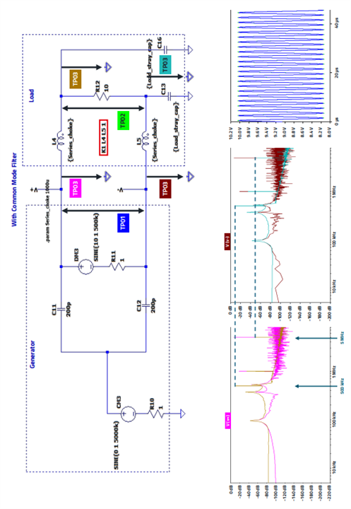
Figure 6: Filter with two inductors in mutual inductive coupling. The signals of TP01 and TP02 overlap in time domain, the signal of TP02 is behind the signal of TP01 in the graph.
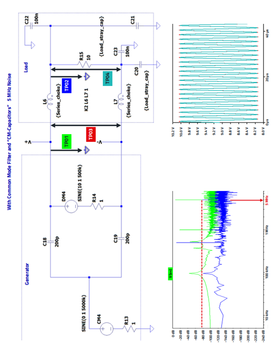
Figure 7: Common mode choke filter with additional Y-capacitors (C22, C23). The signals of TP03 and TP04 overlap in time domain, the signal of TP03 is behind the signal of TP04 in the graph.
Figure 8 shows the influence of the coupling factor K on the attenuation of the DM attenuation, for better visualization the CM source level was set to 0. Figure 8 shows that even a small reduction in the K-factor can have a major effect on the attenuation of the differential signal. In the present simulation, an inductor without the non-linear behavior of the ferrite material on the impedance over the frequency is used. In practice, however, the course of the complex permeability over the frequency and thus the non-linearity of the inductance over the frequency must be taken into account. Furthermore, the parasitic parameters, such as the parasitic capacitances of the windings, must be considered. The first step in acquiring these parameters is to determine the equivalent circuit diagram of the CM choke
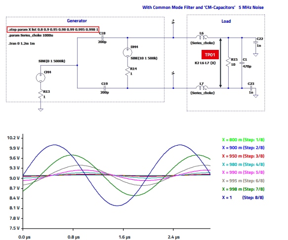
Figure 8: Influence of the K-factor to the DM attenuation.
2.2 Measurement and calculation of the parameters for the equivalent circuit diagram of the CMC.
The equivalent circuit diagram of the choke is required not only for the simulation of the CMC but also for understanding the component if the filter insertion loss is to be considered taking into account the real properties. Data can be taken from the data sheet, but some parameters must also be measured and calculated. The following is a summary. When developing the equivalent circuit diagram of a CMC, the parameters of the equivalent circuit diagram are mainly determined by measurements, which are carried out in three steps. Figure 9 shows the equivalent circuit diagram used here.
The selected common-mode choke is the WE-CMDC, Order Code: 744238132, the data sheet shows the following parameters that can be used to further determine the missing values (Figure 10)
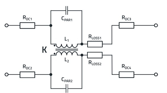
Figure 9: The equivalent circuit diagram of the CM choke used here. The equivalent loss resistance (RLOSS_X), in has been converted here from a parallel circuit to a series circuit
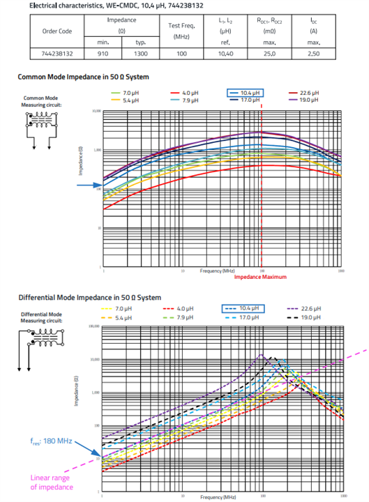
Figure 10: Electrical parameters from data sheet, CM choke WE-CMDC, 744238132
The choke has an inductance per winding of 10.40 µH, the inductance was measured at a frequency of 100 MHz. At this frequency, a scalar impedance in the range of 910 – 1300 Ω is specified. The DC resistance, i.e. the copper resistance of a winding, is a maximum of 25 mΩ.
The blue curve in the upper diagram in Figure 10 shows the CM impedance, which corresponds to the impedance of a winding (L1 or L2) with the ferrite core, as the windings are connected in parallel in the same winding direction. The maximum of the curve (dark blue) is at approx. 100 MHz, the resonance is not very pronounced. A direct linear increase in impedance from 1 MHz is not recognizable, i.e. the ferrite material has a lossy permeable part over the entire frequency range, which leads to the flat curved shape of the curve. The lower diagram in Figure 10 shows the DM impedance. Up to approx. 50 MHz the impedance increase is linear. The diagram also shows a resonant frequency at approx. 180 MHz. The resonant frequency is pronounced, it is caused by the parasitic coupling capacitances of the windings.
In the next step, the impedance of the primary coil is measured, and the ferrite loss resistance and the parasitic winding capacitance are determined. The basic measurement setup and the corresponding equivalent circuit diagram are shown in Figure 11.
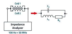
Figure 11: Schematic measurement setup for determining the parameters for the equivalent circuit diagram of the CM choke.
The inductance L0, including the leakage inductance LS, the resistance R0, which corresponds to the ferrite loss, and the leakage capacitance C0 of the winding are measured. R0 and C0 are the total values of the primary and secondary coils. L0 is the sum of the magnetic fluxes generated by the primary and secondary coils. The inductance appears to double, but the primary and secondary coils are connected in parallel, so the result remains L0. The result of the impedance measurement is shown in Figure 12. To determine the inductance, an area of the impedance curve is selected, that is as linear as possible.
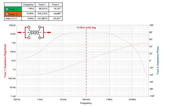
Figure 12: CM impedance of the coil in the frequency range between 100 Hz and 50 MHz, red: impedance, blue: phase.
In this area, the phase shift of the impedance should be over 80°, as this indicates a dominant inductance and capacitive and ohmic losses are negligible. This ensures that the inductance is calculated based on a realistic model. If the inductance were calculated in a range with significant loss components (phase components below 80°), larger deviations could occur, as the loss resistance falsifies the measurement.
The diagram in Figure 12 shows that at 100 kHz the impedance is approx. 12 Ω at a phase angle of 82°. This results in the following calculation:
Z at 100 kHz: 13 , θ = 82°
With
results in:
Resistance R: 1.67 Ω → RO = 3.34 Ω
Inductive Reactance XL: 11.88 Ω
Inductance LO: 18.91 µH
To calculate the leakage inductance, the impedance of the primary coil can be measured with the secondary coil short-circuited. Due to the magnetic coupling, LS is the sum of the leakage inductances of the primary and secondary coils. If the secondary coil is short-circuited, the magnetically coupled L0 is short-circuited from the primary coil's point of view and the residual leakage inductance LS can be measured. The schematic measurement setup is shown in Figure 13.
L0 is the total inductance, consisting of leakage inductance and the inductance L0 ' , which acts on the common mode interference.
This results in the following formula:
 (5)
(5)
Figure 14 shows the measurement protocol for calculating the leakage inductance.
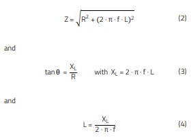
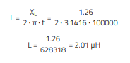
The following calculations are obtained with Z = 1.3 Ω and θ = 76˚ at 100 kHz:
Resistance (R) is calculated using R = Z · cos(θ)
Inductive Reactance (XL) is calculated using: XL = Z · sin(θ)
Inductance (L) is related to XL by: L = XL/(2 · π · f)
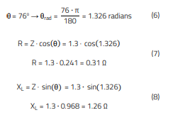
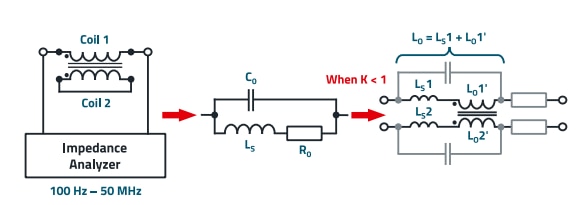
Figure 13: Schematic measurement setup for determining the leakage inductance.
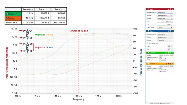
Figure 14: Measurement protocol for calculating the leakage inductance. Red: Impedance, blue: Phase.
 (9)
(9)
Results:
Resistance (R): 0.31 Ω
Inductive Reactance (XL): 1.26 Ω
Inductance (LS): 2.01 µH, which is the stray or leakage inductance, measured at 100 kHz.
The parasitic capacitance is determined at the resonance point of the choke, which is above the frequency of 50 MHz. For this purpose, the insertion loss is measured as shown in Figure 15 using an RF network analyzer.
Three different signal levels were measured in order to take into account any shifts caused by the influence of the ferrite material.
The curves in Figure 15 all show a resonance at 241.77 MHz. The stray capacitance can now be calculated as follows.
With
 (10)
(10)
and
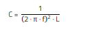 (11)
(11)
and
C0 = 2 · CS; LS = 2 µH
There is:
C0 = 1.26 pF (including all measurement stray effects as well).
The next, very important parameter of a CM choke is the coupling coefficient K or the mutual inductance M. As mentioned before, the coupling coefficient K of a CM choke is a measure of how effectively the magnetic fields of its two windings are coupled. Ideally, for a CM choke, K should be close to 1, meaning the magnetic flux generated by one winding is almost entirely linked with the other winding. This high coupling ensures effective suppression of CM noise while allowing differential signals to pass with minimal interference. But in this case as there will be no stray inductance for filtering DM signal harmonics or noise, an additional inductance must be added. Thus, if the coupling coefficient K is reduced the stray inductance might be useful to reduce the DM noise which of course then must be in the frequency range above the useful signal.
Figure 15: Insertion loss of the DM impedance with three different signal/measurement levels.
The following relationship exists for the parameters K and M:
Coupling coefficient K = (L0 – LS)/L0
Mutual inductance M = K L0
L0 = 18.91 µH
LS = 2.01 µH
This results in the following values:
Coupling coefficient K = 0.89
Mutual inductance M = 16.9 µH
The measurement of the copper resistance RDC at direct current is still missing, which is surprisingly difficult, as this measurement of a very small resistance value depends on the ambient temperature and the test object contact (despite Kelvin terminals). Ultimately, the value was measured under controlled conditions; the setup and measurement results are shown in Figure 16. As the primary and secondary coils have the same number of turns, the measured value also applies to the secondary coil. The value determined for the copper resistance RDC of a winding including the connections is 23 mΩ.
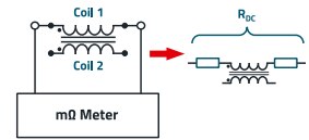
Figure 16: Schematic measurement setup for determining the copper resistance of the windings.
Overall, this results in the following equivalent circuit diagram for the CM inductance (Figure 17).
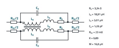
Figure 17: Equivalent circuit diagram of the CM choke WE-CMDC, order code: 744238132.
The influence of the parameters C0 and K on the filter properties are shown below. The circuit diagram shown in Figure 18 is used to show the influence of the parasitic capacitance C0 of the CMC
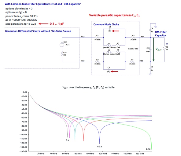
Figure 18: Circuit diagram and output voltage (VOUT) of the filter to show the influence of C0. As this is a simulation, no capacitive stray effects due to measurement set-up are included.
The parasitic capacitance in the windings of this inductor arises from the proximity of adjacent turns of the windings, leading to unintended capacitive coupling. This coupling forms a parallel resonance with the inductance of the windings, creating a self-resonant frequency which is clearly visible in Figure 18. Below the self-resonant frequency, the inductor exhibits primarily inductive behavior, providing effective common-mode noise attenuation. However, as the frequency approaches the self-resonant frequency, the parasitic capacitance causes the inductor's impedance to drop significantly. At frequencies above the self-resonant frequency, the inductor's impedance becomes capacitive, reducing its effectiveness in attenuating CM noise. This shift adversely affects the insertion loss, particularly at higher frequencies, where the inductor no longer provides significant attenuation. As can be seen in Figure 18, even small values of parasitic capacitance such as 0.3 pF lead to strong resonance effects at a frequency in the range of around 115 MHz. This pronounced parallel resonance has a high Q factor. For this reason, the presence of parasitic capacitances can introduce unwanted resonances into the circuit, potentially amplifying certain noise frequencies instead of suppressing them, and easily coupling into neighboring circuits. To mitigate these effects, careful design practices are used, such as selecting the proper inductor, minimizing coupling at the PCB, damping resonances with additional losses like resistors, and adding differential mode SMD ferrites that are lossy in this frequency range. These measures help minimize parasitic capacitance and extend the effective operating frequency range of the inductor.
The circuit diagram shown in Figure 19 is used to show the influence of the coupling factor K, resp. the Mutual inductance M of the CMC over the DM voltage VOUT. A high coupling factor, close to 1, indicates strong magnetic coupling, meaning that most of the flux generated by one winding links with the other.
This enhances the inductance seen by CM currents, improving the inductor's ability to attenuate CM noise. Consequently, the resonant frequency for CM noise is lowered due to the increased effective inductance.
The resonant frequency is primarily influenced by the leakage inductance and the parasitic capacitance. Thus, as shown in Figure 19, a higher coupling factor reduces leakage inductance, which in turn raises the resonant frequency. With a higher K, the inductor provides better CM noise attenuation across a broader frequency range before reaching resonance.
Additionally, the insertion loss for CM noise improves because the inductor remains effective at higher frequencies. Conversely, if K is low, the leakage inductance increases, lowering the resonant frequency and potentially reducing the effective frequency range for noise suppression. This may also result in a lower insertion loss at higher frequencies.
In practical applications, a CMC needs to be selected which balances high coupling for effective noise suppression with a proper selected leakage inductance to prevent unintended impacts on DM signals
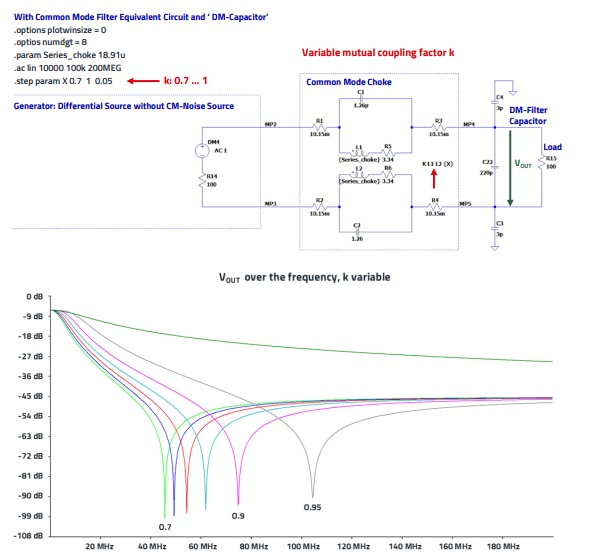
Figure 19: Circuit diagram and output voltage (VOUT) of the filter to show the influence of M (K).
3. FILTER APPLICATIONS
The following section presents practical examples that demonstrate the use of CM chokes. These applications are straightforward and highlight the benefits of CM chokes when their design and parameter selection are carefully optimized.
3.1 Common Mode Filter
Figure 20 shows the schematic of a simple CM filter. To show the effects of selecting different values of the WE-CMDC series the insertion loss was measured. The filter is built on a breadboard with a GND layer; the GND layer was omitted in the area of the CM choke in order to keep the capacitive coupling small. The input signal is a differential signal with an impedance of 50 Ω to ground, i.e. 100 Ω differential impedance. The output was fed to the oscilloscope via a differential probe with 1 MΩ differential input impedance. Figure 21 shows the DM attenuation. The double logarithmic diagram in Figure 21 shows that the differential attenuation is low for all selected values up to approx. 5 MHz. Beyond this frequency rage, the attenuation depends not only on the selected inductance value, but also on the behavior of the imaginary part of the permeability µ'' of the ferrite material. Of course, the filter with the higher inductance also shows a higher attenuation, but the non-linearity, especially the kink at approx. 35 MHz, is due to the ferrite material. Above 35 MHz, the attenuation increases significantly for all 4 filters, as the ferrite material comes closer to its resonant frequency and thus its higher impedance range where not only µ', but also µ'' increases significantly.
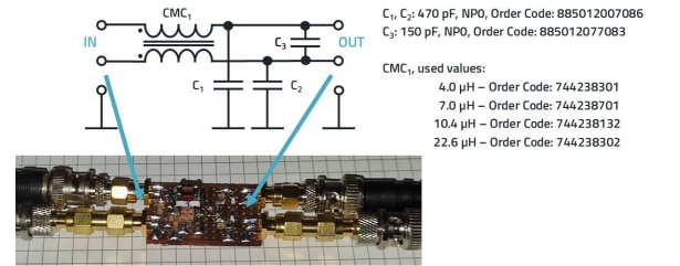
Figure 20: Schematic and setup of a CM filter, using different common mode chokes of the WE-CMDC series. “IN” is the side on which the measurement signal (in practice the interference signal) was applied.
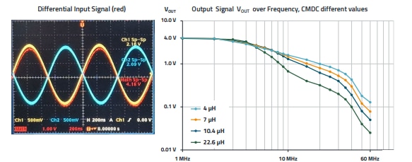
Figure 21: DM attenuation of the filter, shown in Figure 20.
Mutual inductance (M) decreases with frequency as the ferrite’s real permeability (µ') drops, increasing LSTRAY and DM attenuation. The ferrite’s imaginary permeability (µ'') increases at higher frequencies, introducing resistive losses that further enhance DM attenuation. Although LSTRAY behaves like an air-core inductor, its value is influenced by the frequency-dependent coupling (M) with the core material. As a result, DM attenuation depends on the ferrite material because its permeability variations affect both LSTRAY and resistive losses across the frequency range.
The CM attenuation is shown in Figure 22. A higher inductance leads to a higher impedance, the markers each show the 3 dB cut-off frequency. All chokes show no pronounced resonances, in the range around 80 MHz there is a weak parallel resonance due to the design. In the range between 200 MHz and 300 MHz the impedance turns the chokes into the capacitive range, the impedance increases. This range is also determined by the measurement assembly and can vary depending on the layout and setup.
Nevertheless, in the 50 Ω system of the network analyzer, with all inductance values, the setup enables at least an insertion loss of 40 dB at 100 MHz, with the 22.6 µH choke over 50 dB.
3.2 Coupled Filter for noise reduction in DC-DC converters
Noise on the outputs of DC-DC converters can originate from several sources, including high-frequency switching transients, conducted and radiated electromagnetic interference (EMI), and ripple voltage due to imperfect filtering. The switching process in pulse-width modulation or pulse-frequency modulation converters generates high-frequency noise that can couple into sensitive circuits. Insufficient filtering or improper PCB layout can exacerbate these noise issues, leading to signal integrity problems. When this noise propagates into circuits, it can cause malfunctioning of analog and digital components, leading to instability, erroneous data processing, or degraded performance. High ripple voltage can interfere with precision analog circuits, introducing offset and reducing accuracy in sensor readings or ADC conversions. In RF systems, noise from DC-DC converters can increase phase noise, reducing overall system sensitivity. For high-speed digital systems, excessive noise can result in timing errors and communication failures.
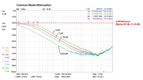
Figure 22: CM attenuation of different chokes in the range from 500 kHz to 1 GHz, measured in the 50 Ω-system with a network analyze.
An additional filter, which is constructed from a CM choke in a special switching mode, can effectively reduce residual interference, Figure 23 shows the circuit diagram.
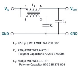
Figure 23: DC-Line filter for additional noise attenuation with WE-CMDC as a coupled inductor. “VIN” is the side on which the measurement signal (in practice the interference signal) was applied.
By coupling the second winding to ground, an additional reduction in noise can be achieved. One parameter for a high attenuation is of course the inductance of L1, another is the mutual coupling factor, which should be in the range below 0.9 as the stray inductance determines the attenuation. The higher the capacitance of C1, the lower the frequency range that can be attenuated. A typical value is 220 µF, which can be used to filter into the kHz range. The ESR of the capacitor should be low, which is why a polymer capacitor was used. Some measurement signals to illustrate the effectiveness are shown in Figure 24.
The signal attenuation at 1 MHz is approx. 73 dB; if capacitor C1 is removed, the attenuation is reduced by approx. 6 dB. This reduction in attenuation is practically constant from 200 kHz up to 30 MHz.
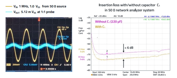
Figure 24: Signal attenuation and insertion loss of the filter with coupled inductor.
3.3 Oscillator with very low distortion
If you turn the CM inductor by 90 degrees in the circuit, you get a signal transformer. Of course, the CM choke was not manufactured for this application, but the “usefulness” of the component for this application can easily be checked. Figure 25 shows the transfer characteristic of the 22.6 µH choke over frequency.
Of course, the signal transformer can only be used in a frequency range in which the transmission characteristics are good, i.e. the linearity is high, and the losses are lowest. According to Figure 25, this is the range between approx. 80 kHz and 2 MHz.
The following application shows the use of the CMC choke as a signal transformer in a Meissen oscillator. The Meissen oscillator circuit generates sinusoidal oscillation. It consists of an amplifier (e.g. a transistor) and a signal transformer (two coupled coils), which serve as a frequency-determining element. The positive feedback to generate oscillation is realized by the inductive coupling between the coils of the transformer. The oscillation frequency is determined by the inductance of the transformer and the capacitances in the circuit. The oscillator is easy to set up and offers a stable oscillation generation with a high output amplitude. The frequency can be easily adjusted by changing the inductance or capacitance. As the output at C2 is not decoupled, any capacitive load at C2 changes the resonant frequency. R3 decouples the resonant circuit and thus mitigates the effects of capacitive loads on the resonant frequency.
Figure 26 shows the schematic, the set-up and the output signal of the circuit.
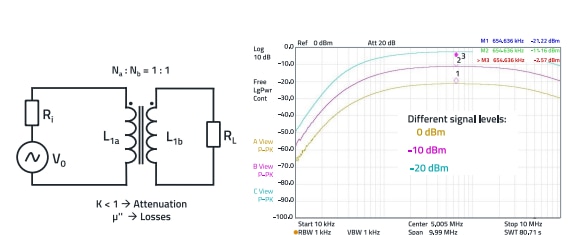
Figure 25: Transfer characteristic of the CM choke if used as a signal transformer with the turn ratio 1:1 (Na:Nb)
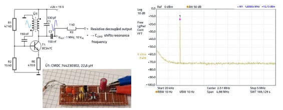
Figure 26: Schematic and the output signal of the Meissen oscillator.
With a supply voltage of 15 V, the output voltage is 10 Vpp into a 1 MΩ oscilloscope probe. The output signal has a frequency of 1 MHz, and the spectrogram shows that the harmonics of the signal are in the noise, thus having a distance to the fundamental signal of more than 60 dB. This makes the circuit very interesting for applications where high signal purity is required.
3.4 Primary DC-filter, common- and differential mode
The last application in this article is the use of WE-CMDC in a DC input filter, i.e. the classic common mode choke. However, transient and reverse polarity protection are also taken into account in this application (Figure 27).
What is important here is a low-offset-interference, low-impedance connection to the primary ground (SGND) for the effectiveness of the "Y-capacitors" to effectively attenuate the CM interference. It is also important to ensure that the transition from SGND to GND on the secondary side of the CM choke is done at a controlled connection on the metal housing. For a detailed description, please refer to the reference design RD041.
4. CONCLUSION
It has been shown that a CMC choke with a ferrite core is an effective measure for suppressing CM interference in electrical and electronic circuits. However, it is important to understand that inductance is not the only parameter that needs to be considered in terms of signal characteristics. The frequency-dependent permeability of the ferrite material and the parasitic capacitance of the choke change the characteristics. Careful selection of the choke, taking into account the frequency of use and the specific application, is therefore crucial. The application areas of a CMC may well go beyond the typical areas such as EMC filters in power supply units. Nevertheless, optimal design requires consideration of all electrical and mechanical properties to ensure effective function.
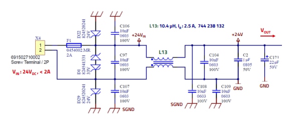
Figure 27: Schematics of a DC-filter with CM and DM attenuation.
A APPENDIX
Finally, Figure 28 in the Appendix provides a comprehensive overview of typical inductors used in signal applications. The focus is primarily on common-mode chokes, complemented by SMD ferrites and hinged ferrite series. This comparison aims to help the user better understand the key differences, advantages, and specific applications of each component, enabling more informed and effective selection.
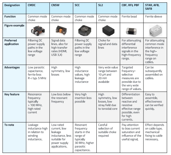
Figure 28: Overview of typical Inductors for Signal Applications: Common-Mode Chokes, SMD Ferrites, and Hinged Ferrite Series
IMPORTANT NOTICE
The Application Note is based on our knowledge and experience of typical requirements concerning these areas. It serves as general guidance and should not be construed as a commitment for the suitability for customer applications by Würth Elektronik eiSos GmbH & Co. KG. The information in the Application Note is subject to change without notice. This document and parts thereof must not be reproduced or copied without written permission, and contents thereof must not be imparted to a third party nor be used for any unauthorized purpose. Würth Elektronik eiSos GmbH & Co. KG and its subsidiaries and affiliates (WE) are not liable for application assistance of any kind. Customers may use WE’s assistance and product recommendations for their applications and design. The responsibility for the applicability and use of WE Products in a particular customer design is always solely within the authority of the customer. Due to this fact it is up to the customer to evaluate and investigate, where appropriate, and decide whether the device with the specific product characteristics described in the product specification is valid and suitable for the respective customer application or not. The technical specifications are stated in the current data sheet of the products. Therefore the customers shall use the data sheets and are cautioned to verify that data sheets are current. The current data sheets can be downloaded at www.we-online.com. Customers shall strictly observe any product-specific notes, cautions and warnings. WE reserves the right to make corrections, modifications, enhancements, improvements, and other changes to its products and services. WE DOES NOT WARRANT OR REPRESENT THAT ANY LICENSE, EITHER EXPRESS OR IMPLIED, IS GRANTED UNDER ANY PATENT RIGHT, COPYRIGHT, MASK WORK RIGHT, OR OTHER INTELLECTUAL PROPERTY RIGHT RELATING TO ANY COMBINATION, MACHINE, OR PROCESS IN WHICH WE PRODUCTS OR SERVICES ARE USED. INFORMATION PUBLISHED BY WE REGARDING THIRD-PARTY PRODUCTS OR SERVICES DOES NOT CONSTITUTE A LICENSE FROM WE TO USE SUCH PRODUCTS OR SERVICES OR A WARRANTY OR ENDORSEMENT THEREOF. WE products are not authorized for use in safety-critical applications, or where a failure of the product is reasonably expected to cause severe personal injury or death. Moreover, WE products are neither designed nor intended for use in areas such as military, aerospace, aviation, nuclear control, submarine, transportation (automotive control, train control, ship control), transportation signal, disaster prevention, medical, public information network etc. Customers shall inform WE about the intent of such usage before design-in stage. In certain customer applications requiring a very high level of safety and in which the malfunction or failure of an electronic component could endanger human life or health, customers must ensure that they have all necessary expertise in the safety and regulatory ramifications of their applications. Customers acknowledge and agree that they are solely responsible for all legal, regulatory and safety-related requirements concerning their products and any use of WE products in such safety-critical applications, notwithstanding any applicationsrelated information or support that may be provided by WE. CUSTOMERS SHALL INDEMNIFY WE AGAINST ANY DAMAGES ARISING OUT OF THE USE OF WE PRODUCTS IN SUCH SAFETYCRITICAL APPLICATION.
DIRECT LINK
ANP146 | Theoretical Insights and Practical Applications of the WE-CMDC Series Common Mode Chokes
USEFUL LINKS:
Application Notes : https://we-online.com/en/support/knowledge/application-notes
Services: https://we-online.com/en/products/components/service
Contact : https://we-online.com/en/support/contact
CONTACT INFORMATION
Würth Elektronik eiSos GmbH & Co. KG
Max-Eyth-Str. 1, 74638 Waldenburg, Germany
Tel.: +49 (0) 7942 / 945 – 0
Email: appnotes@we-online.de
