Application Note
Design of a Single Pair Ethernet System with Power over Data Lines (SPoE)
RD041 by Dr.-Ing. (Doctor of Engineering) Heinz Zenkner
1. INTRODUCTION
This reference design note describes a system that can transmit data between two points via a two-wire line. The main unit supplies the peripheral unit with power via the same two-wire line over which the data is transmitted. This method is called "Single Pair Ethernet" with "Power over Data Lines".
Thus, SPE (Single Pair Ethernet) with PoE (Power over Ethernet) - PoDL (Power over Data Lines) is a technology that combines data transmission and power delivery over a single twisted pair cable. Single Pair Ethernet (SPE) is an emerging standard for Ethernet communication that utilizes only one pair of wires for data transmission, unlike traditional Ethernet which typically uses four pairs. This makes SPE suitable for applications where space and weight are constrained, such as in automotive, industrial, and IoT (Internet of Things) devices.
Power over Ethernet (PoE) is a technology that allows electrical power to be transmitted alongside data over Ethernet cables. This eliminates the need for separate power cables, simplifying installation and reducing costs, especially in applications like IP cameras, VoIP phones, and wireless access points. Power over Data Lines (PoDL) extends the concept of PoE to Single Pair Ethernet (SPE) by enabling power delivery over the single twisted pair used for data transmission in SPE systems. This allows devices connected via SPE to be powered over the same cable used for data communication, further simplifying cabling infrastructure and reducing complexity in deployments.
2. BASIC SET-UP, FEATURES AND REQUIREMENTS OF A SPOE SYSTEM
The single pair with PoE, or SPoE as it is abbreviated in some literature, is different in definition and implementation compared to PoE. It contains,
- A unique power coupling technique used in a 2-wire circuit.
- A simultaneous transmission of power and data over a balanced twisted pair.
The data connections are realized via single pair of wires, AC-coupled at each end to avoid ground loops. The PoE Fsystems transmit power in common mode to the data, the SPoE systems diplex power and data over a single pair of conductors. Figure 1 shows a principal diagram of the SPoE system.
On the left side of the diagram in Figure 1 is the power source equipment (PSE) with the PHY.

Figure 1: Principal diagram of the SPoE system.
On the right side there is the powered equipment (PD, load) and another PHY. The PHYs provide the data link and the PSE provides the power to the PD. The data link is decoupled capacitively (C1 – C4) and the power inductively (L1 – L4). Both, data, and power are transferred via the twisted pair cable. The interface is called “Media dependent interface” or “port interface” (MDI/PI).
The integration of power delivery alongside data transmission demands a robust classification-based Power Delivery Protocol, designed to ensure compatibility between Power Sourcing Equipment (PSE) and Powered Devices (PD). The protocol employs a series of steps to establish compatibility and safety before delivering power, thus mitigating the risk of potential hazards such as short circuits or open circuits. The protocol initiates with the detection phase by the PSE, where it identifies the presence of connected PDs within the network. Following this, the PSE proceeds to classify the PD, requesting essential information such as class and type. Additionally, the protocol incorporates Cable Resistance Measurement (CRM), supported by the PD, to further assess the integrity of the connection. The protocol is defined in IEEE 802.3cg (SPoE, 2019), which is an extension of the 802.3bu Power over Data Lines (PoDL, 2016) standard. PoDL defines protocols for detection, classification, and power-up procedures, ensuring a standardized approach across various networking environments. Moreover, SPoE extends its capabilities to encompass long-reach protocols, exemplified by 10BASE-T1L, with the potential to span cable lengths of up to 1 kilometer. This opens doors to a multitude of applications, particularly in scenarios where traditional power delivery methods may be impractical or inefficient. The SPoE electrical requirements are specified in the following IEEE standards:
- IEEE 802.3cg (10BASE-T1): Bandwidth 0.1 to 20 MHz, reach up to 1000 m.
- IEEE 802.3bw (100BASE-T1): Bandwidth 0.3 to 66 MHz, reach up to 40 m.
- IEEE 802.3bp, (1000BASE-T1): Bandwidth 1 to 600 MHz, reach up to 40 m.
As shown in Figure 2, the cables used for SPoE differ from the standard cables used for Ethernet.
SPoE requires cables which are defined in IEC 61156 which is „multicore and symmetrical pair/quad cables for digital communications“. Standard CAT 6 or CAT 7 cables even if shielded, are not suitable.
As with the Ethernet classes, there are different variants of SPoE, which are shown in Table 1 below.

Figure 2: Layout of cables for standard Ethernet and for SPoE.

Table 1: Overview of SPE/SPoE available variants and their capabilities. BER: Bit error rate, the number of bit errors per unit time (s). UTP: Unshielded Twisted Pair. STP: Shielded Twisted Pair.
IEEE 802.3bu is a standard adopted by the IEEE in 2016 for powering devices over a single-pair Ethernet connection. The cables vary depending on the application, cables type A include solid wires for permanent installation, type B cables have wires with stranded conductors for flexible applications or vibrations. SPoE can be integrated into a mixed system with common industrial Ethernet protocols such as Ethernet/IP, Profinet, and EtherCAT and can deliver a simultaneous power supply to end devices. Figure 3 shows a possible set-up.
The PSE tests the link before turning on the power. Checking, using a 10 mA test current, if the voltage drop is within a specified range. If the PD is found, the device class is determined by a so called “Serial Communication Classification Protocol” (SCCP). After having determined the PD-class the power is ramped up. Depending on the system, supply voltages can be 12 V, 24 V, 48 V and power classes reach from 0.5 W to 50 W at a maximum current of 2 A. When not providing full power, the PSE continuously sources below 1 mA at 3.3 V (Sleep Mode). Table 2 shows the physical layer parameters of SPoE systems.
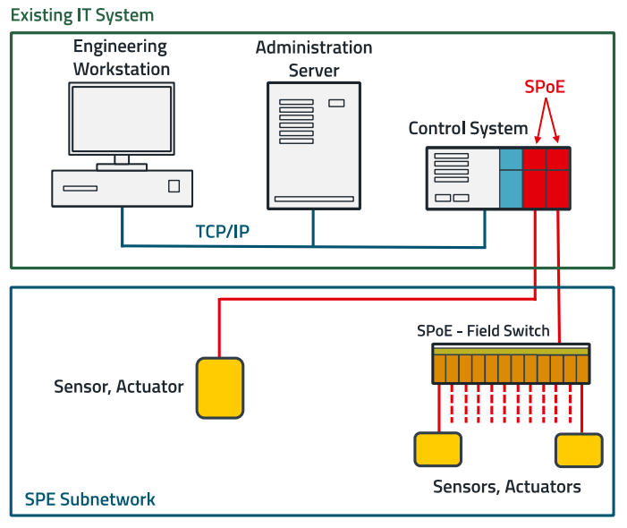
Figure 3: Extension of an existing IT-system by SPoE.
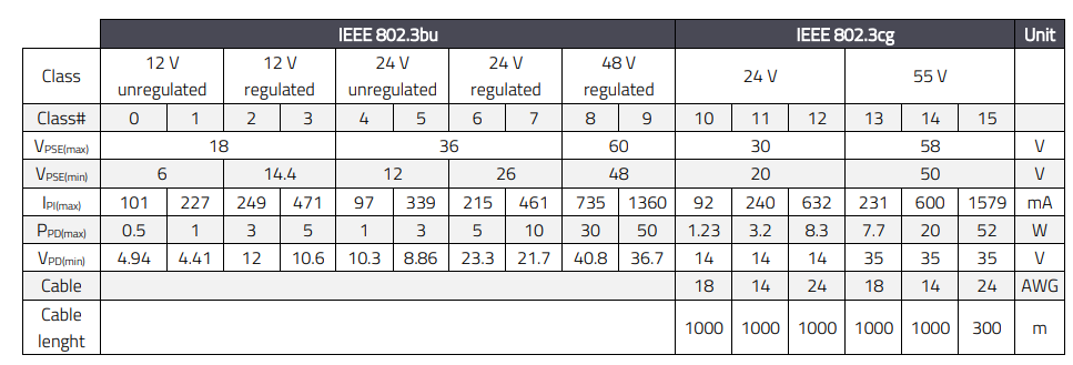
Table 2: Physical layer parameters of SPoE systems.
3. THE HARDWARE TOPOLOGY OF A SPOE SYSTEM
Figure 4 shows the hardware topology of a SPoE system. On the left side is the PSE, on the right the PD and in between the transmission path, i.e. the cable. The interfaces with primary transient protection, CM chokes, transformers, and secondary transient protection to PHY are the same for the PSE and the PD.
Power and data are coupled together at the interface through a power coupling network. The PHY is AC-coupled by the data transformer T1. CMC1 attenuates common mode noise from the data line to the PHY and vice versa. The PSE DC power is coupled onto the differential data lines and decoupled by CMC2. CMC2 is wired in such a way that the differential DC current does not saturate the choke, so that the signal opposes the impedance of each choke winding package and is thus decoupled. The magnetics (T1, T2, CMC1, CMC2) must be selected to meet the droop, return loss, and mode conversion specifications according to IEEE 802.3cg. For the transient protection at the input of the interface, thus at the primary side of the transformers T1 and T2, the ground reference is the housing, “earth ground”. For the transient protection at the secondary side of the transformers, the reference ground GND_sec. is the ground for the PHY protection.
Conventional IEEE 802.3 multipair Ethernet (including PoE) requires galvanic isolation from the chassis ground. According to IEEE 802.3bu (PoDL) and IEEE 802.3cg (SPoE) standards, PSE/PDs must provide at least 1 MΩ (@ 5 V ± 20%) isolation between all accessible external conductors and the interface (MDI). Depending on the application, the equipment must comply with relevant standards such as IEC 61010-1 (Safety regulations for electrical measuring, control, and laboratory equipment) or IEC 62368-1 (Safety requirements for equipment for audio/video, information, and communication technology). Devices with no electrically conducting pins, except the twisted-pair Ethernet MDI, can meet isolation requirements by using a nonconductive chassis enclosure.
For SPoE applications requiring galvanic isolation from the chassis, an isolated power supply must be utilized. Relevant safety standard requirements including clearance and creepage distances, as well as protective distances, must be adhered to.
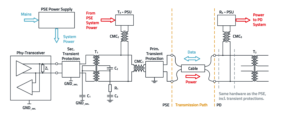
Figure 4: General interface block diagram of the SPoE system.
4. THE WÜRTH ELEKTRONIK SPOE-SYSTEM
The block diagram of the system is shown in Figure 5. The System is powered from an external power supply at the PSE (connector X4, +24 V / < 80 mA). By definition, the power supply system is not galvanically isolated. If galvanic isolation is necessary due to the application, this must be ensured by the external 24 V supply. The following devices can be connected to the PSE and PD for data communication:
- PSE/X7: 10 Mbit/s Ethernet → PD/X7: 10 Mbit/s Ethernet
- PSE/X1: USB 3.1 → PD/X1: USB 3.1
The interfaces can be in mixed or cross configuration and operated at the same time. Additionally, the operating status can be monitored on the PSE/X9. X9 is a serial interface and for simple operation a serial/USB converter should be used, which is then connected to the USB interface of a PC. The setup is explained in more detail in chapter 6.
The SPE transmission path operates at a data rate of 10 Mbit/s with an amplitude of approx. 2.5 VSS, the operating voltage on the two-wire line is 20 to 24 VDC. Figure 6 shows the voltage and data under operating condition.
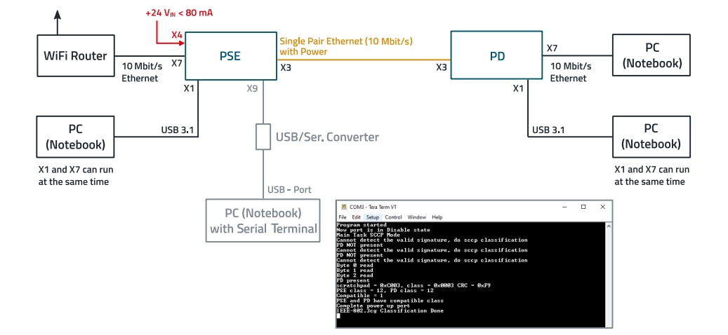
Figure 5: Block diagram of the Würth Elektronik SPoE-system.
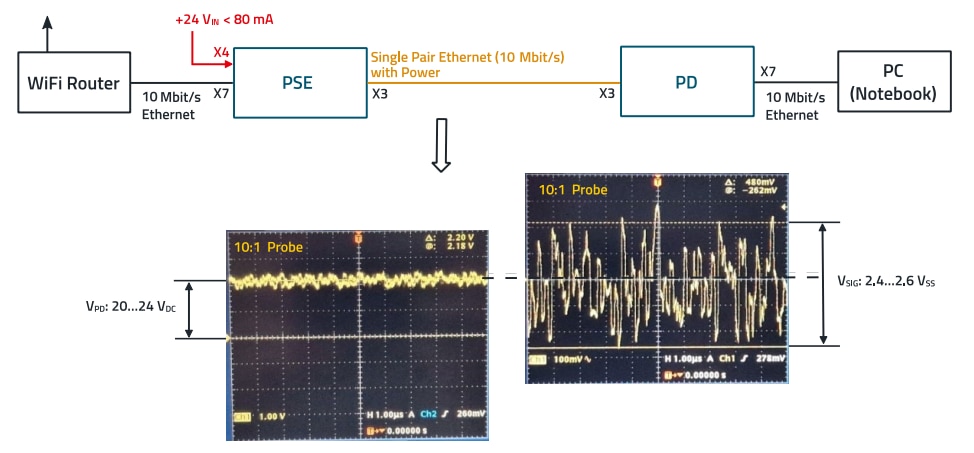
Figure 6: Voltage and data on the SPE-wires.
5. HARDWARE DESCRIPTION
5.1 PSE (Power Source Equipment)
Block diagram and features of the PSE
The data is transferred from the SPoE interface to the PHY ADIN1100. The PHY converts the data and forwards it to the LAN9355 Ethernet switch. The multiport Ethernet switch forwards the data to both the Ethernet port and the LAN7800 Ethernet/USB converter (see Figure 7). The power supply for the PD is coupled into the SPoE interface via a network. The IEEE 802.3cg-compliant control of the power supply takes place via the LTC4296 controller and is managed by the STM32G03C8T6 microcontroller. The power supply as such is fed into the LTC4296. A DC-DC converter generates a +3.3 V voltage from the +24 V to supply the onboard SPE electronics.
The characteristics of the PSE can be summarized as follows:
- Supports multiple power levels of Power over Ethernet
- Detecting and classifying the PD, sourcing the right amount of power to the PD
- PoDL class 12 up to 30 V / 8.3 W
- USB 3.1 port (no power)
- 10 / 100 Mbit/s Ethernet port
- 10 Mbit/s SPE port
- Data transfer between USB 3.1 and 10 / 100 Mbit/s Ethernet
- Data transfer between USB 3.1 and SPE (10 Mbit/s)
- Data transfer between SPE (10 Mbit/s) and 10 / 100 Mbit/s Ethernet
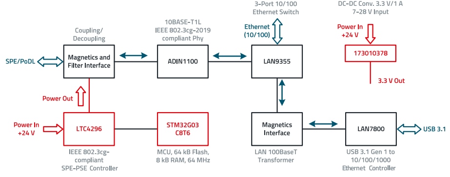
Figure 7: Block diagram of the PSE board.
In Figure 8 the top side of the PSE board is shown. The SPoE interface is located on the left-hand side. The connection can be made either via a 3-pin plug-in terminal (X3) or an SPE connector (X2). The 24 V power supply connection (X4) is located at the bottom left of the image and the Ethernet (X7) and USB interfaces (X1) are located on the right-hand side.
The picture also shows that the electronic ground has been separated from the connector/housing ground and the connection can be made via numerous components. As with the GB-Ethernet designs, this concept was chosen in order to be able to choose between different grounding concepts depending on the housing (metal/plastic). The variations are explained in more detail in the following chapters.
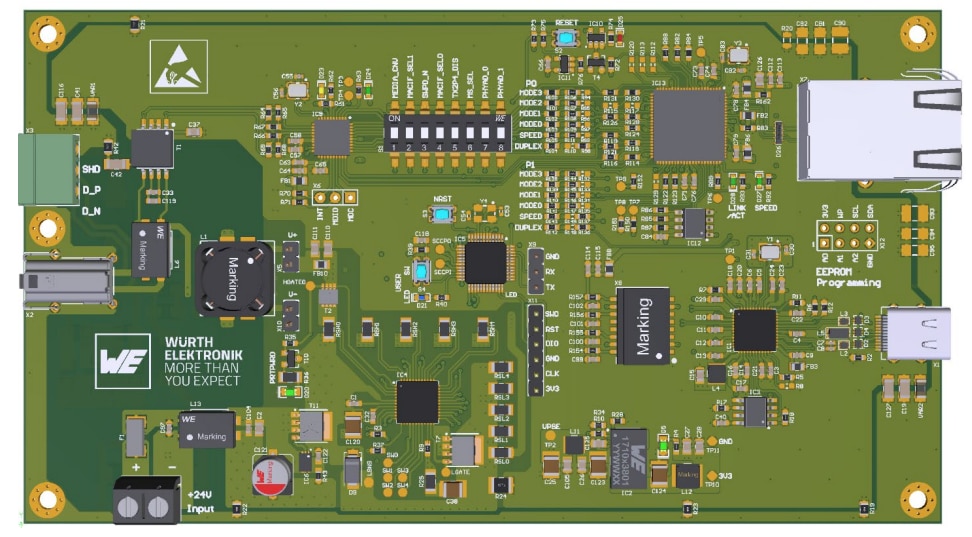
Figure 8: Top side of the PSE board, on the left is the SPE-Interface, connection can be made alternatively via 3-pin plug in terminal or SPE-connector.
PSE-Interface to SPoE
Figure 9 shows the schematic of the SPoE interface at PSE side. On the primary side at the center tap of the transformer T1, capacitors C33 and C119 are used for galvanic isolation to prevent direct current from the applied supply voltage of +24 V through the transformer. Furthermore, resistor R42 ensures termination with an impedance of 100 Ω via capacitors C42, C116 and C41. The circuit also ensures balancing in the event of any imbalance in the signal voltage.
The SPE signal pair can be connected to either connector X2 or X3. The Varistor VAR1 reduces any residual charges in the cable or on the capacitors when the system is not in operation, or the cable is removed from the interface. Resistor R29 is fitted as an alternative to VAR1, C41 and C116 if the electronics board is to be installed in a plastic housing, as in this case there is no stable ground reference for a lowimpedance function of VAR1, C41 and C116.
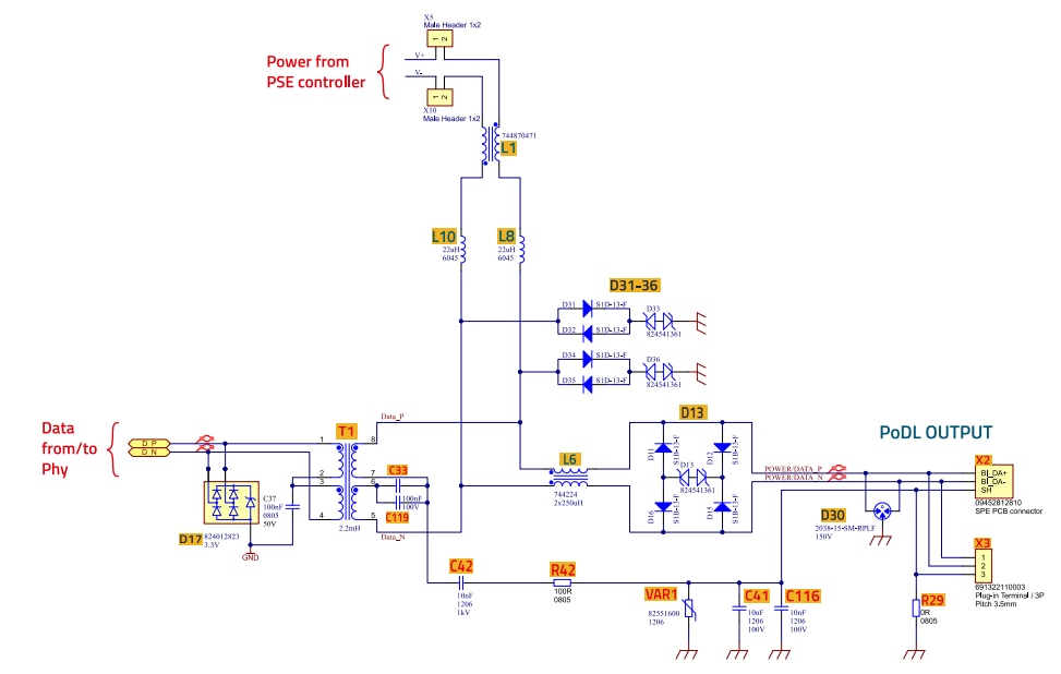
Figure 9: SPoE interface at PSE side.
The CM choke L1 is connected in such a way that it provides a high impedance for both, the noise of the DC supply current and the differential signal current. It should be noted here that this choke is pre-magnetized by the supply current to the PD and therefore a choke with an appropriate rated current must be selected. L8 and L10 are additional inductors to decouple the power supply from the system to increase the signal to noise ratio of the Ethernet signal and for EMC reasons due to the system design. The CM choke L6 reduces CM interference coming from the cable side (e.g. transients) and reduces any high-frequency interference generated by the PHY and power supply system in the direction to the cable. The choke should have a low leakage inductance so as not to impair the signal too much. Transient protection is an important task at the interface, as the possible length of the transmission line means that the coupling of transient interference must be taken into account. Effective transient protection that can absorb high power is therefore required on the primary side. A three-stage limitation of transient overvoltage is provided in this design. The first stage is realized with a symmetrical gas-plasma arrester (D30). The arrester limits the transient voltage between the signal wires and earth from approx. 350 V and thus absorbs most of the energy of the pulse in common mode. The second stage is the TVS diode D13 with its steering diodes D11, D12, D15 and D16. This circuit clamps at approx. 58 V, in case differential mode transient overvoltage occurs between the signal wires. The third stage is constructed after choke L6 with TVS diodes D33, D36 and diodes D31, 32, 34 and D35.
Like the second stage, this stage limits at 58 V (plus diode forward voltage), but with each line to earth, so that the common-mode voltage remaining behind the choke can be safely limited to protect the DC-DC controller, which can withstand a maximum input voltage of 80 V. In the direction of the signal path, the TVS diode array D17 is provided on the secondary side of the transformer T1. The ground reference of the TVS diode array is the PHY IC9, in order to protect the signal inputs in the event of transient common mode voltages of > 4.5 V.
What is the purpose of the diodes provided in addition to the TVS diodes? TVS diodes in the high-power range have a high parasitic capacitance, for example the bidirectional TVS diode D13 WE-TVSP 824541361, with approx. 700 pF at 24 V. This capacitive load is too high for the signal. Therefore, the fast recovery diodes D11, 12, 15, 16, S1B-13-F, which have a parasitic capacitance of only 10 pF, are looped-in to reduce the total capacitive load in differential mode to reduce the capacitive load to < 10 pF. As mentioned, the TVS diode used here has a break down voltage of 42 V and a clamping voltage at 58 V, in case of the transient event, twice the forward voltage VF of the Diodes must be added.
It should be pointed out once again that this protection is differential from line to line. Most transient disturbances will occur in common mode. Therefore, the additional protection with D33 and D36 has been implemented, which limits the common mode transients. The clamping circuit consists of the TVS Diodes D33, D36 WE-TVSP 824541361 and the Diodes D31, 32, 34, 35, SID-13-F. The Diodes again reduce the parasitic capacitance as serial components, the line-to-line capacitance is approx. 10 pF, which is neglectable. On primary side of the transformer T1 all circuits are directly connected to the shield ground (e.g. housing) to achieve a low parasitic impedance for a low voltage offset which, if too high, may impair the proper function of the clamping process.
Figure 10 shows the PCB layout of the SPoE interface at PSE side. X2 and X3 are the connections for the signal/power supply cable. The transient protection was placed on the bottom side of the PCB to minimize the length of the tracks to the diodes. The inductive components L6, T1 and L8 / L10 are positioned next. In this area of the PCB, no ground filling was used to minimize capacitive coupling and thus achieve a higher filter/clamping effect.
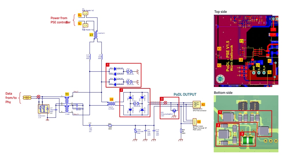
Figure 10: Layout of the SPoE interface at PSE side.
PSE-Controller and Power Supply On the PSE side, the power supply for the system is fed in at connection X4 (Figure 11). The following transient protection with D1 limits overvoltage to 33 V in differential mode, D22 and D29 clamp transient voltages above 28 Vin common mode. The three capacitors before and after the CM choke L13 form a πfilter with the choke to attenuate high-frequency interference in both directions, i.e. from the PSE board to the power supply connection and from the power supply connection in the direction of the PSE board.
The circuit with the MOSFET T11 and IC6 replaces a Schottky diode, but with the advantage of generating virtually no voltage drop. The IC controls the voltage drop in the forward direction via the MOSFET to ensure uniform current output without oscillation even at low loads. If a current source fails or is short-circuited, a fast switch-off minimizes the reverse current transients. Due to its wide operating voltage range, the circuit can also withstand a reversed input voltage of up to 80 V. If the circuit is not required for application reasons, it can be omitted completely, and a wire jumper can be used at T11from source to drain.
The LTC4296-1 (IC4) is an IEEE 802.3cg-compliant, fivechannel Power over Ethernet (SPoE) controller with a PSE power supply unit.
The controller is designed for interoperability with 802.3cg powered devices (PDs). In this design, only one of the five channels is required. High-side protection with MOSFET T2 and analogue current limiting enable controlled switch-on and short-circuit protection, tapped via RSH0. The low-side protection with T7 and via RSL0 protects the negative output against regenerative faults and earthing faults. PD classification via the serial communication classification protocol (SCCP) ensures that the full operating voltage is only applied to the cable if a PD is present. The SW0 pin switches off the port power snubber via T5 during detection and classification. The controller is steered via SPI with the microcontroller. T3 / T8 and T6 are switched via the microcontroller and are used for SCCP control.
The capacitor C34 and the resistor R13 represent a defined impedance when the snubber C35/R14 is switched off via T5. This reduces resonances and overshoots during load jumps. Diode D10 protects the circuit in the event of forced reverse voltages. The π-filter with C110, FB10 and C111 attenuates high-frequency interference signals, especially in the 10 MHz range and above. FB10, WE-CBF 742792031, is an SMT ferrite with a broadband impedance curve.
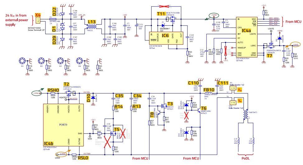
Figure 11: Schematic of the power supply and PSE controller.
As only one of the five available channels is used, the four unused channels must be wired as shown in Figure 12, thus connected to the power supply + VPSE / LSNS as well. This configuration is essential for the function of the controller. The current sense resistors RSHx/RSLx must be routed via “Kelvin-Sense” connections like shown in Figure 12 on the right-hand side. The reason is to achieve the specified current-threshold accuracy.
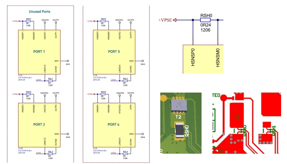
Figure 12: Wiring of the unused channels of the LTC4296-1 and the “Kelvin-Sense” routing of the Sense resistors RSHx/RSLx.
RESET Circuit, DC-DC and PSE-Microcontroller (MCU)
Figure 13 shows the circuit of the +24 V to +3.3 DC-DC controller and the circuit around IC5, an STM32G030C8T6 microcontroller. IC11 is the reset circuit controlled by the microcontroller, the red LED D25 shows the RESET status. The push-button S2 is the RESET for SPoE, LAN and USB controllers, S3 for the PSE-controller (MCU). S4 is not in operation during normal mode and only for FW debugging purpose. The microcontroller controls the PHY ADIN1100 on the one hand and the PSU controller LTC4296 (SCCP protocol and timing) on the other with its firmware.
The DC-DC controller IC2 is a variable step-down module which offers high efficiency and delivers up to 3 A of output current. It operates with an input voltage from 3.5 V to 38 V. The module includes a “Spread Spectrum” option which jitters the switching frequency by +/-5% and thus spreads the harmonics generated by the converter over a wider bandwidth per time in order to “relatively” reduce the interference emission related to a specified measuring bandwidth of the measurement receiver (9 kHz, 120 kHz).
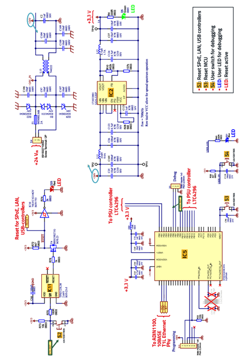
Figure 13: Schematics of Microcontroller, Reset circuit and +24 V to +3.3 V DC-DC controller.
Let's go back to the +24 V input of the system. The module has a shield ground (SGND) and a system ground (GND). The π-filter refers to the SGND, the electronics after the filter to GND, as shown in Figure 14. The circuit has placement options R19 to R23 between SGND and GND.
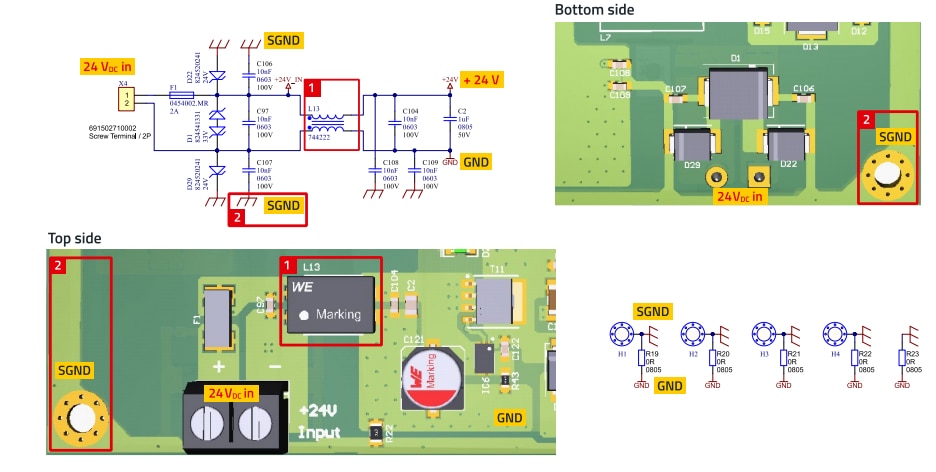
Figure 14: +24 V input of the system with SGND-GND connections.
Depending on the housing and grounding system, the system can be adapted in terms of EMC behavior using different component variants. The component locations R19 to R23 can be bridged with 0 Ω resistors, so that the SGND has the same reference potential as the GND.
However, it is also possible to equip R19 to R23 with SMT ferrites and thus, e.g. in a metal housing, keep the housing ground at SGND, but separate the electronics GND at high frequency and reduce interference if necessary. The main purpose of these components here in the reference design is to test the shielding properties of cables and set-up variants during the EMC tests.
Ethernet PHY at PSE side
The ADIN1100 is a 10BASE-T1L transceiver for industrial Ethernet applications (Figure 15). The controller is compliant with the IEEE 802.3cg-2019 Ethernet standard for single-pair Ethernet (SPE) with a long range of 10 Mbit/s. The ADIN1100 supports a cable range of up to 1700 meters with Auto Negotiation enabled.
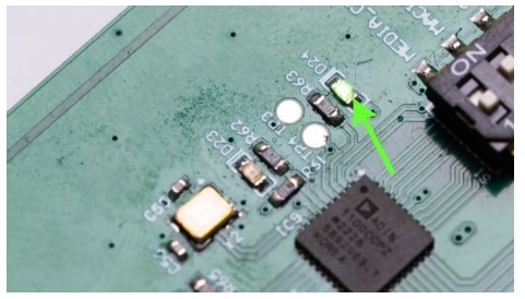
The PHY core supports the 1.0 V p-p operating mode and the 2.4 V p-p operating mode defined in the IEEE 802.3cg standard; the voltage mode is displayed by LED D23 (yellow). The MDIO interface is a 2-wire serial interface for communication with a microcontroller. The interrupt PIN of the ADIN controller has been connected additionally to X6 for having the possibility for connection of an external debugger. The hardware configuration of the PHY is configured via the dip switches S1. The link up/activity is displayed by LED D24 (green).
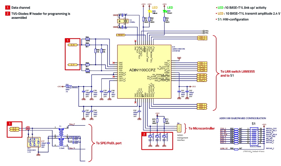
Figure 15: Schematic of the Ethernet-PHY at PSE side.
LAN switch and Ethernet port
The LAN9355 controller is used here to distribute the data coming from the SPoE-PHY ADIN1100 to a 10 / 100 Mbit/s Ethernet port and via an Ethernet/USB controller (LAN7800) to a USB 3.1 interface. Figure 16 shows the circuit diagram. The LAN9355 is a 3-port 10 / 100 Ethernet switch for embedded applications. The controller includes all the features of a 10 / 100 switch system, including the switching arrangement, packet buffer, buffer manager, media access controllers (MACs), PHY transceiver and serial management. Each of the three ports is fully compliant with the IEEE 802.3 standard and all internal MACs and PHYs support full/half-duplex 10BASE-T and 100BASE-TX operation. The integrated I2C and SMI slave controllers allow full serial management of the controller via the integrated I2 C and MII interface respectively.
The controller has four power supply connections, each of which is filtered separately (FB2, FB4, FB6, FB5). The green LEDs D27 and D28 indicate the data traffic and the link active. The Ethernet interface includes transient protection with the TVS diode array D26, which is located between the LAN transformer and the Ethernet controller.
The task here is to limit the transient overvoltage coming from the cable, which occur on the secondary side of the transformer in common mode, against the ground of the controller. The resistors R77 to R81 are 50 Ω terminations, on the signal lines 2 × 50 Ω differential to ground via the capacitors C112, C113 and C126.
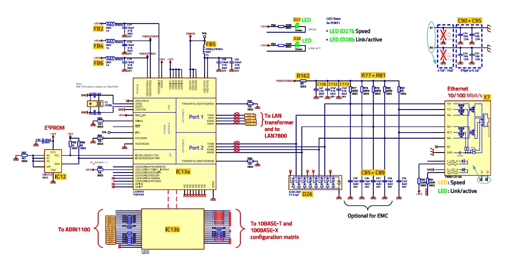
Figure 16: Schematic diagram of the LAN-switch and the Ethernet port at PSE side.
At the same time, a DC voltage decoupled via R162/C112/C113/C126 is fed in via the resistors to operate the controller's output drivers in "current mode". Figure 17 shows the layout of the Ethernet interface. The capacitors C85 to C89 (number 3) are optional to reduce high frequency noise which could be radiated via the Ethernet cable. The Ethernet connection block X7 contains the transformers as well as the CM chokes and the Bob Smith termination.
As already explained in the previous chapter, the ground system can be configured via the component locations C90 to C95 (number 4). The termination resistors and the EMCcapacitors (number 2 and 3) are assembled on the bottom side to reduce any parasitic impedances as much as possible. The TVS-diode array D26 is routed directly into the signal path for optimized effectiveness. As D26 protects the inputs of the controller, the reference GND must be the GND of the controller.
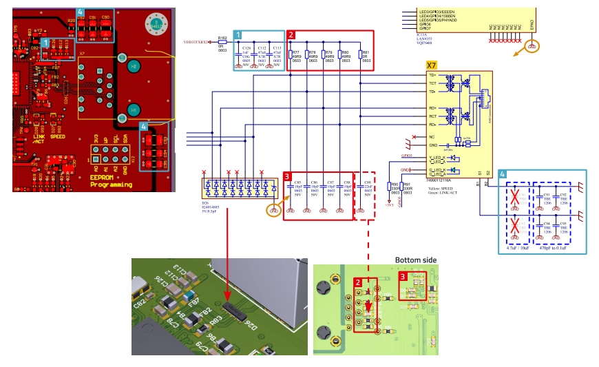
Figure 17: Layout of the Ethernet interface at PSE side.
Ethernet – USB 3.1 bridge
The used LAN7800 (IC1) is a 1 GB-Ethernet, highperformance USB 3.1 controller with integrated Ethernet PHY. An external 4 kbit EEPROM was connected for the onboard software. The circuit diagram is shown in Figure 18. The lower part of the controller in the figure is the signal section (IC1A), clocked with a 25 MHz quartz (Y1); the upper part is the controller’s relatively complex chip-internal power supply (IC1B).
In order to maintain signal integrity, a transformer module for matching (X8) was inserted between the Ethernet port of the LAN7800 and the LAN switch. On the primary side towards LAN7800 of the Transformer module the Bob-Smith termination is included, on the secondary side 50 Ω-resistors are implemented to match the necessary system impedance.
The capacitors C114and C115 connect the resistors HF-technically to the reference ground. The connection to the supply voltage via the SMT ferrite FB8supplies the input/output of the LAN switch, which is operating in current mode here. For a detailed description of the USB 3.1. to Ethernet bridge, please refer to the Design-Note RD016.
The USB 3.1 interface is critical in terms of immunity to fast transients such as ESD or burst. For this reason, several points must be taken into account in the design, which are explained next (refer to Figure 19). The power supply connection is not needed here, the “VBUS” pins of the connector are left open. Transient protection is provided directly at the connector plug, the reference ground for the TVS diodes D2 to D4 is the ground of the connector and the housing, i.e. the floor of the room in relation to the ESD interference source.
The board fastenings H1 to H4 must be made with screws with low impedance to the housing. The resistors R19 to R23 are placeholders; if a metal housing is used, 10 nF / 200 V capacitors can be used; if a plastic housing is used, 0 Ω resistors should be soldered in. Depending on the ground concept of the overall device, it may also be necessary to use an SMT varistor in places where the reference ground has a high interference potential due to interfering electronics, for example.
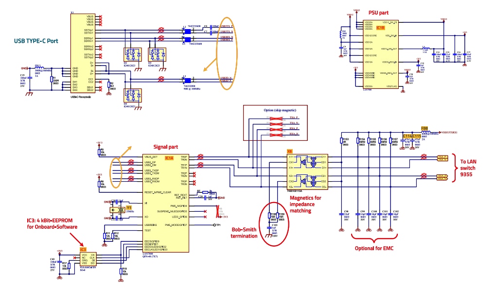
Figure 18: Schematic of the USB 3.1. to Ethernet bridge at PSE side.
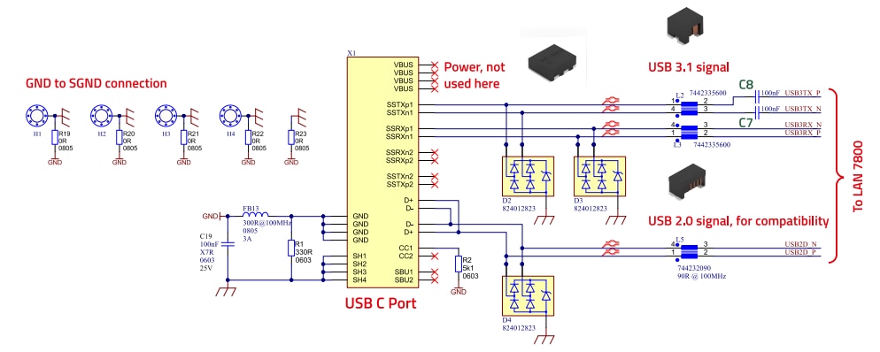
Figure 19: Schematic of the USB 3.1. interface at PSE side.
This is also the reason why the resistor R1 (330 Ω) is not used when a metal housing is used and the filtering of the GND line in the USB cable takes place via FB13 and C19. Here too, the reference ground for C19 is the housing. Figure 20 shows the layout of the USB 3.1. interface. The components are routed in signal flow to achieve the lowest possible parasitic coupling.
The signal trances are guided directly via the TVS-Diodes to minimize parasitic inductances between the ground connection of the TVS-Diodes and the housing ground (SGND). The signal trances need to meet the symmetrical system impedance of 90 Ω.
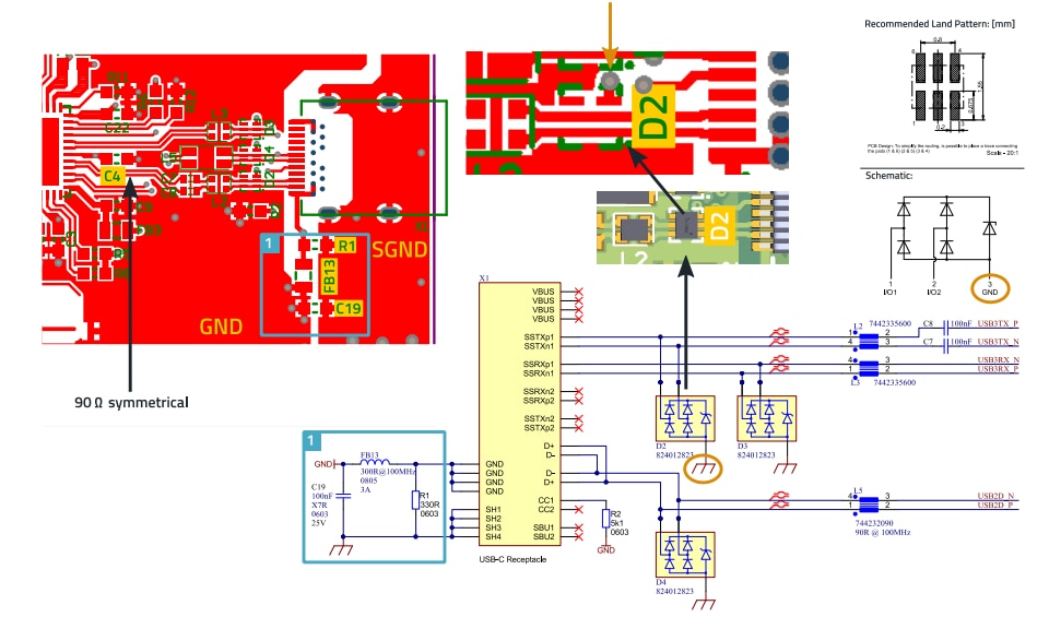
Figure 20: Layout considerations of the USB 3.1. interface.
5.2 PD (Powered Device)
Block diagram and features of the PD
The signal flow at PD side is the same as in the PSE-design. As shown in Figure 21, the data, coming from the SPE is transferred from the SPoE interface to the PHY ADIN1100. The PHY then converts the data and forwards it to the LAN9355 Ethernet switch.
The multiport Ethernet switch then forwards the data to both the Ethernet port and the LAN7800 Ethernet/USB converter. The power supply, coming via cable from the PSE is coupled into the SPoE PD controller LTC9111. The IEEE 802.3cg-compliant controller takes care of the SCCP-based classification. A DC-DC converter generates a 3.3 V voltage from the +24 V to supply the onboard PD electronics.
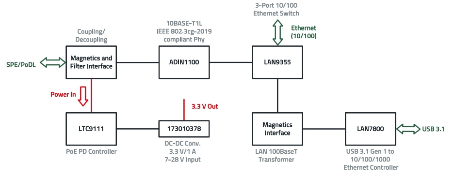
Figure 21: Block diagram of the PD board.
The characteristics of the PD can be summarized as follows:
- Operating voltage: 24 V, power classification via SCCP protocol.
- USB 3.1 port, self-powered device (no power on port).
- 10 / 100 Mbit/s Ethernet port.
- 10 Mbit/s SPE port.
- Data transfer between USB 3.1 and 10 / 100 Mbit/s Ethernet.
- Data transfer between USB 3.1 and SPE (10 Mbit/s)
- Data transfer between SPE (10 Mbit/s) and 10 / 100 Mbit/s Ethernet.
In Figure 22 the top side of the PD board is shown. The SPoE interface is located on the left-hand side. The connection can be made either via a 3-pin plug-in terminal or an SPE connector. The Ethernet and USB interfaces are located on the right-hand side.
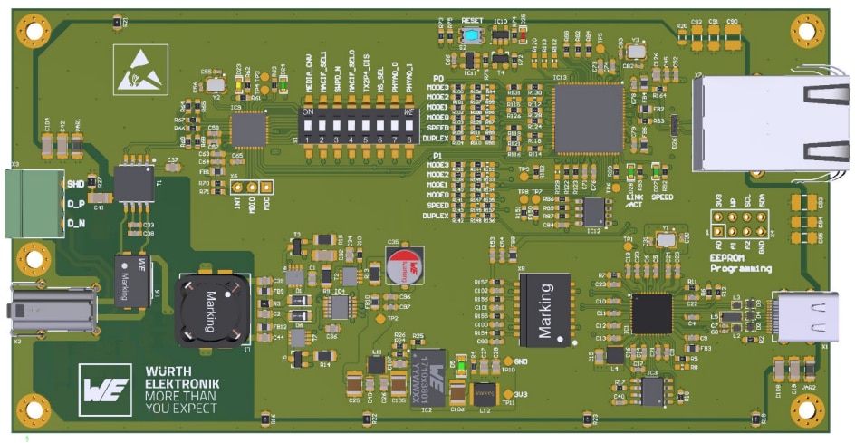
Figure 22: Top side of the PD board, on the left is the SPE-Interface, connection can be made alternatively via 3-pin Terminal or SPE-connector
PD-Interface to SPoE
Figure 23 shows the SPoE interface of the PD, which is in principle identical to the PSE interface.
The only difference is that the PD separates the signal from the power supply, unlike the PSE, where the two components signal and power supply are "mixed".
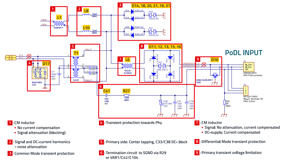
Figure 23: SPoE interface at PD side.
SPoE-PD controller and Power Supply The supply current decoupled in the filter is fed to the power supply system with the SPoE controller LTC9111, the schematic is shown in Figure 24. The Schottky diodes D1and D6 provide a "correction" of the DC polarity. The MOSFET T2 isolates the output from the input during SCCP classification. IC2 is the DC-DC buck converter with spread spectrum, explained in the chapter 5.1 about the SPE already. The filters marked with red boxes in the circuit diagram decouple the circuit at high frequency and thus reduce EMC interference caused by the controller and by the following electronics.
The classification of the PD class is set by the PINs 4, 5 and 10 at the controller, the table in Figure 24 shows the corresponding PD class. Figure 25 shows a section of the circuit shown in Figure 24. The MOSFETs T6 and T7 are for the low side power rectification, SNS1 and SNS2 are the port voltage sense before the power rectification for the SCCP and state machine voltage thresholds. T3 and T5 are used for the SCCP signaling. R3 is the wire termination for damping resonances, C2 blocks DC current. C1 is an additional AC ripple attenuation, R9 with C32 is a snubber for damping resonance with the differential inductance of the power coupling network. The total capacitance (C1 and C32) should be more than 150 nF, a too small capacitance creates resonances with the parasitic inductances of the system (magnetics, wires/cables).
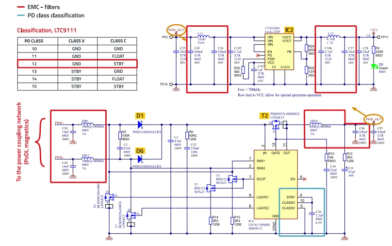
Figure 24: PoE-PD power supply with controller LTC9111.
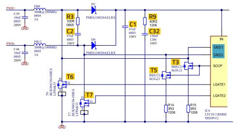
Figure 25: Section on left-hand side of the circuit shown in Figure 24.
The next figure (Figure 26) shows the right-hand side of the circuit shown in Figure 24.
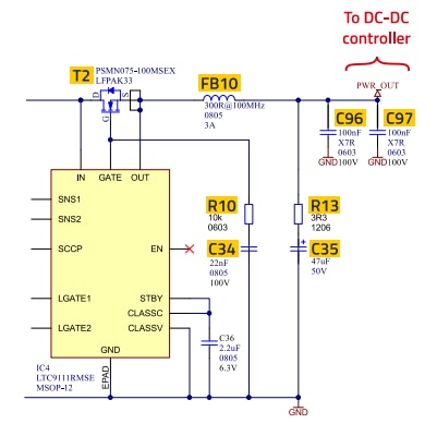
Figure 26: Section on right-hand side of the circuit shown in Figure 24.
FB10 and C96/C97 is the already mentioned EMC filter, for attenuation of AC dynamics, compensation of large transient load changes and buffering energy supply fluctuations from the PSE. R13 with C35 have been implemented as a bypass filter.
R10 with C34 form a low pass for smoother switching of the Gate of the MOSFET T2.
Ethernet PHY at PD side
The controller ADIN1100 has already been described in the chapter 5.1 on the PSE the circuit diagram for the PD side is shown in Figure 27.
Here are just a few additional comments on the circuit diagram. Like most highly integrated controllers, this one also has several supply connections. These should be individually blocked or buffered with capacitors as close as possible to the PINs. Furthermore, as here with the FB1, the IC supply should be decoupled from the voltage system via an inductor (SMT ferrite, RFI inductor) so that interference signals generated by the controller are kept away from other circuits. Which inductor is best suited here is explained in detail in Application Note ANP129.
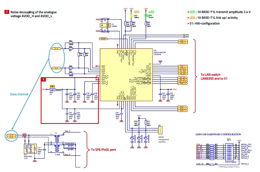
Figure 27: Schematic of Ethernet PHY at PD side.
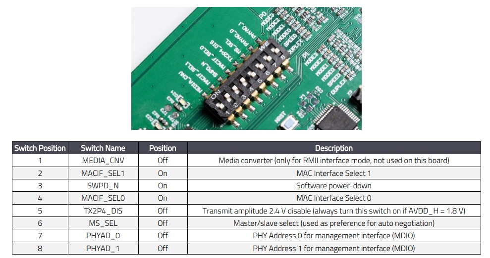
Figure 28 shows the setting options for the hardware configuration via the switches on S1.

Figure 28: Setting options for the HW-configuration via S1.
With regard to the layout, short and symmetrical 50 Ω tracks should be used in the 25 MHz crystal range, as shown in Figure 29.
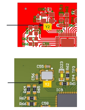
Figure 29: Layout area around the crystal of the ADIN1100.
The area around the crystal and the decoupling capacitors should be filled with GND, which should then be plated through several times to the GND layer so that it does not float.
LAN switch and Ethernet port at PD side
The circuit diagrams are identical to those of the PSE but let us say a few words about the power supply circuit around the switch. The LAN switch LAN9355 has two internal voltage regulators:
- Core regulator for the main core digital logic, the I/O pads, PHYs’ digital logic and for the PHY analogue sections.
- Regulator for the internal oscillator.
The internal DC-DC regulators can be activated via the REG_EN pin (7). Accordingly, a voltage of 1.2 V is applied to the VDDCR (6) and OSCVDD12 (3) outputs (Figure 30). Additionally, there are five different voltage supply sections to be connected and decoupled to each other. For an overview of the power supply connections refer to Figure 31. The LAN switch also has a 25 MHz crystal whose layout area must be carefully designed (Figure 31). See also the description of the Ethernet PHY ADIN1100 here.
The rules for the component selection are the same as mentioned in the chapter about the Ethernet PHY ADIN1100.
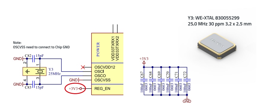
Figure 30: 25 MHz crystal oscillator of the LAN switch LAN9355.
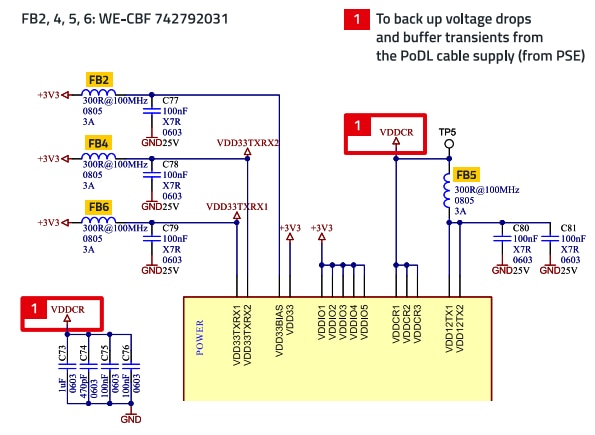
Figure 31: Power supply connections of the LAN switch LAN9355.
Regarding the Ethernet port (Figure 32), C85 to C88 capacitors for HF attenuation (number 4) are also provided, same as in the schematic of the PSE. The capacitors C126, C45, C52 and C89 (number 2) block the RF signals against GND to provide a clean current for the current mode load resistors (number 3).
R164 (number 1) should be a 0 Ω resistor otherwise in case of a ferrite bead to the controllers internal DC voltage causes EMI issues. R77 to R80 (number 3) are firstly for the power supply of the push-pull drivers in the LAN9355 and secondly for the respective impedance termination of 50 Ω, i.e. 2 × 50 Ω balanced to GND. Accordingly, the Ethernet conductor paths must also be designed symmetrically with an impedance of 2 × 50 Ω to ground, i.e. 100 Ω to each other.
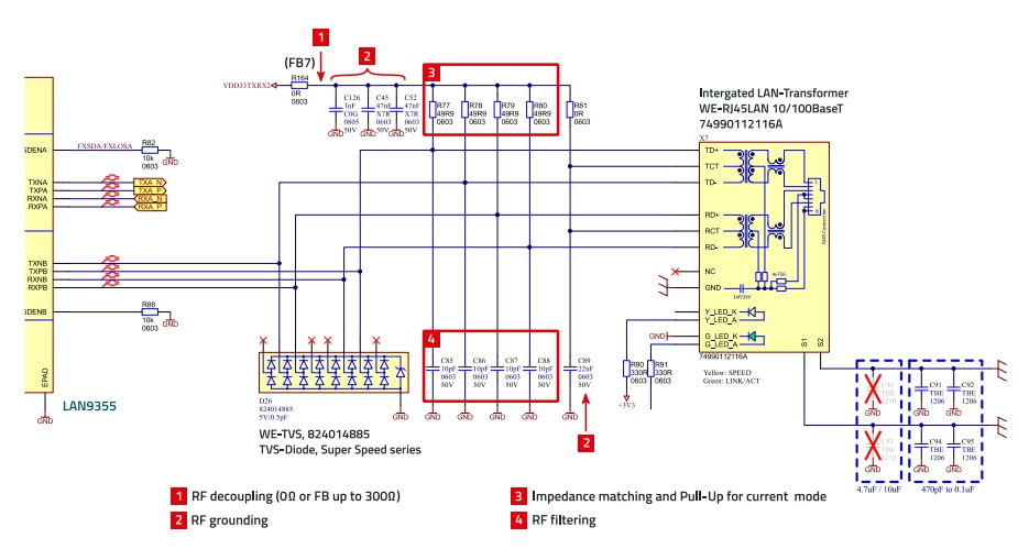
Figure 32: Ethernet port of the PD, with LAN switch LAN9355.
Ethernet – USB 3.1 bridge at PD side
The section is identical to that of the SPE, and the component designations have also been adopted, so that reference can be made here to this section of the document about the PSE. For reference the schematic of the Ethernet – USB 3.1. bridge is shown in Figure 33.
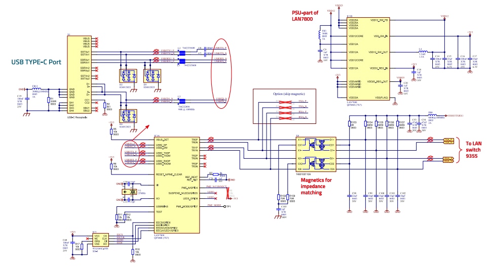
Figure 33: Schematic, Ethernet – USB 3.1. bridge at PD side.
For the layout, which differs a bit from the PSE, some hints should be given regarding the GND/SGND configuration. As shown in Figure 34, the shielding concept may be configured in dependance of the housing. In case of a plastic housing FB13 and C19 should be 0 Ω-resistors, R1 can be kept open.
In case of a metal housing again R1 should not be placed, FB13 and C19 should be placed like shown in the schematic. In the end the assembly variants depend on the overall system and need to be tested in the EMC lab with the whole product.
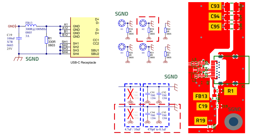
Figure 34: Layout of the USB 3.1 interface area at PD side.
6. INSTALLATION, SET-UP DESCRIPTION
6.1 Equipment to prepare
- 1 × PSE board
- 1 × PD board
- 1 × USB-to-serial adapter with cable
- 1 × WiFi-router
- 1 x PC/NB
- 1 × LAN/Ethernet cable
- 1 × USB3.2 type C to type A cable
6.2 Setup the WiFi-router and connect to internet
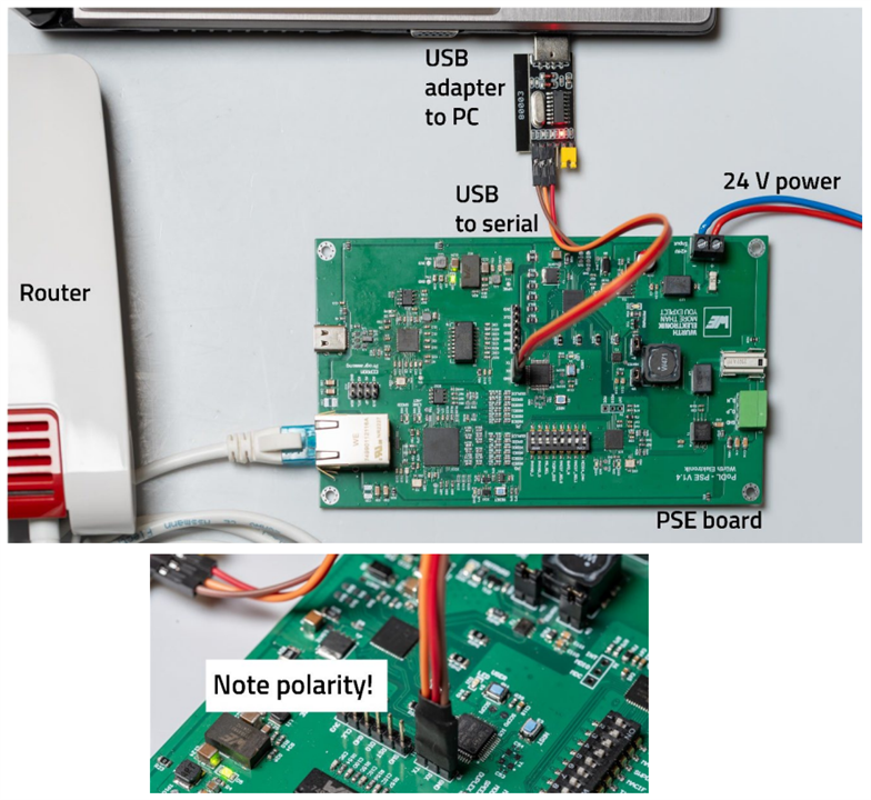
6.3 Setup the PSE board
1. Connect power +24 V to X4.
2. Connect PSE board to router via LAN cable.
3. Connect USB-to-serial adapter with cable to X9.
6.4 Set up serial terminal on PC
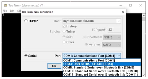
1. Use “Tera Term” or any similar terminal.
https://teratermproject.github.io/index-en.html
2. After opened Tera Term, select COM port to “USB-SERIAL” then click “OK”
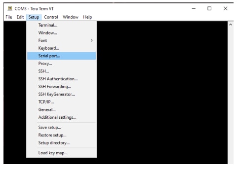
3. Select tap “Setup” and then “Serial port”
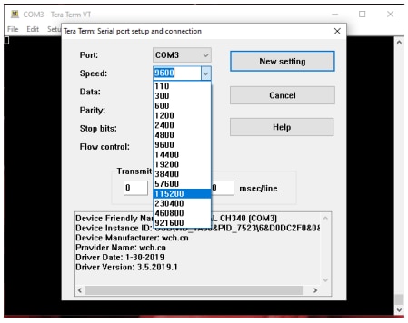
4. Select speed to “115200” then click “New setting”.
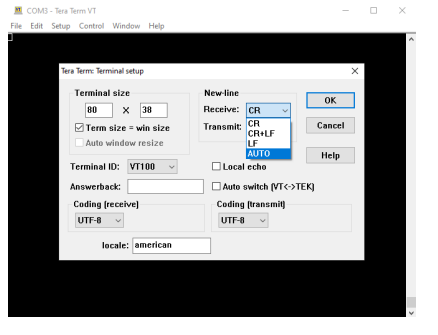
5. Select tap “Setup” and then “Terminal”.
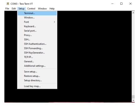
6. At “Receiver”, select "AUTO” then click “OK”.
6.5 Power on the PSE board (+24 V)
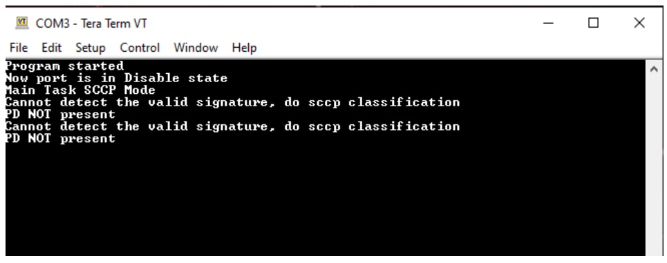
If the settings are correct, the serial terminal will print-out the status as below. The message shows that the PSE works in SCCP mode, no PD device connected.
6.6 Connect the PD board to the PSE
- Connect X2 of both boards via SPE-cable or alternatively --> 6.2.
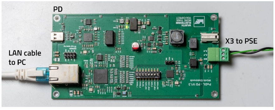
- Connect X3 of both boards via 3 wire cable, like shown in the figure below.
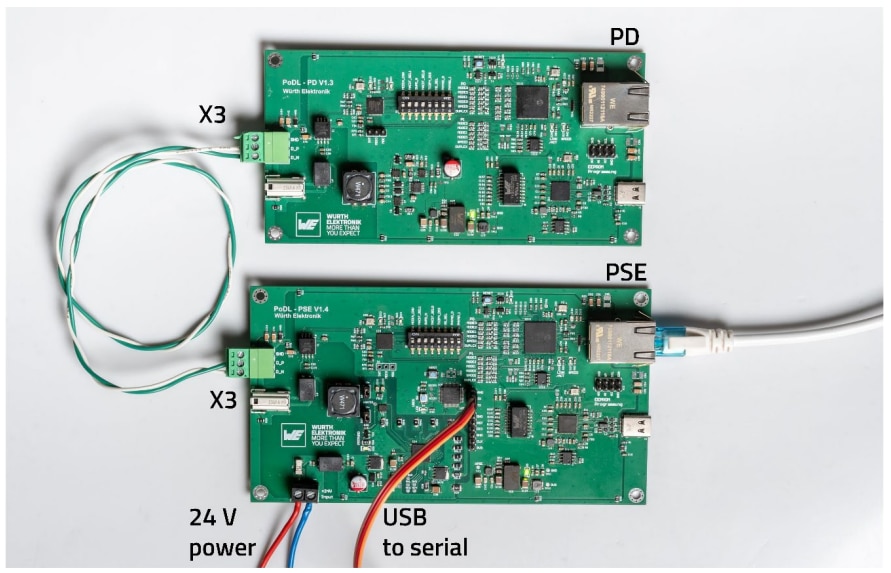
- If the power +24 V from the PSE board is supplied to the PD board correctly, LED D20 (PRTPWR0) on PSE board (left figure) will light-up, LED D5 (+3.3 V) on PD board (right figure) will light-up

and serial terminal will show the status as on the figure below.
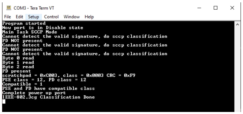
If the communication between the PSE and the PD works, LED D24 of both boards will be blinking.
6.7 Connect PD board to PC
- Via LAN cable
- Connect a LAN cable between PD board and PC.
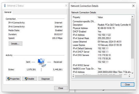
- Check if the PC can get the IP address from the router.
- Via USB-C cable.
- Connect an USB 3.2 type C to type A cable between PD board and PC
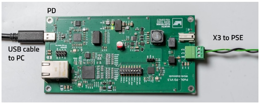
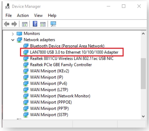
- On PC, open the Device Manager to make sure if the PD board is connected and works properly.
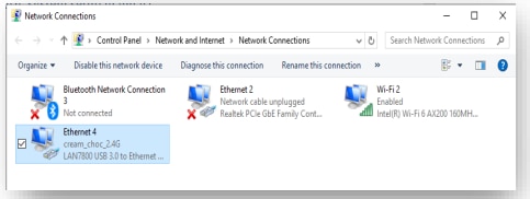
- Open “Network connections” and make sure that the PC connects to the “LAN7800 USB 3.0 to Ethernet 10 / 100 / 1000 Adapter”.
- Check if the PC can get an IP address from the router.
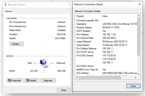
- Open any internet browser and check if the internet connection works.
6.8 PSE and PD HW-Configurations
PSE and PD On-Board Dip-Switch for HW configuration (S1)
PSE On-Board LEDs status

PD On-Board LEDs status

Further information
For further information about the system set-up and EMC tests please refer to the Application Note ANP141 available for download at the Würth Elektronik Home Page.
A APPENDIX
A.1 References
[1] GB Ethernet design: RD016
[2] GB Ethernet design with PoE: RD022
[3] Links to Description of the Firmware, Altium Job Files: RD041
IMPORTANT NOTICE
The Application Note is based on our knowledge and experience of typical requirements concerning these areas. It serves as general guidance and should not be construed as a commitment for the suitability for customer applications by Würth Elektronik eiSos GmbH & Co. KG. The information in the Application Note is subject to change without notice. This document and parts thereof must not be reproduced or copied without written permission, and contents thereof must not be imparted to a third party nor be used for any unauthorized purpose. Würth Elektronik eiSos GmbH & Co. KG and its subsidiaries and affiliates (WE) are not liable for application assistance of any kind. Customers may use WE’s assistance and product recommendations for their applications and design. The responsibility for the applicability and use of WE Products in a particular customer design is always solely within the authority of the customer. Due to this fact it is up to the customer to evaluate and investigate, where appropriate, and decide whether the device with the specific product characteristics described in the product specification is valid and suitable for the respective customer application or not. The technical specifications are stated in the current data sheet of the products. Therefore the customers shall use the data sheets and are cautioned to verify that data sheets are current. The current data sheets can be downloaded at www.we-online.com. Customers shall strictly observe any product-specific notes, cautions and warnings. WE reserves the right to make corrections, modifications, enhancements, improvements, and other changes to its products and services. WE DOES NOT WARRANT OR REPRESENT THAT ANY LICENSE, EITHER EXPRESS OR IMPLIED, IS GRANTED UNDER ANY PATENT RIGHT, COPYRIGHT, MASK WORK RIGHT, OR OTHER INTELLECTUAL PROPERTY RIGHT RELATING TO ANY COMBINATION, MACHINE, OR PROCESS IN WHICH WE PRODUCTS OR SERVICES ARE USED. INFORMATION PUBLISHED BY WE REGARDING THIRD-PARTY PRODUCTS OR SERVICES DOES NOT CONSTITUTE A LICENSE FROM WE TO USE SUCH PRODUCTS OR SERVICES OR A WARRANTY OR ENDORSEMENT THEREOF. WE products are not authorized for use in safety-critical applications, or where a failure of the product is reasonably expected to cause severe personal injury or death. Moreover, WE products are neither designed nor intended for use in areas such as military, aerospace, aviation, nuclear control, submarine, transportation (automotive control, train control, ship control), transportation signal, disaster prevention, medical, public information network etc. Customers shall inform WE about the intent of such usage before design-in stage. In certain customer applications requiring a very high level of safety and in which the malfunction or failure of an electronic component could endanger human life or health, customers must ensure that they have all necessary expertise in the safety and regulatory ramifications of their applications. Customers acknowledge and agree that they are solely responsible for all legal, regulatory and safety-related requirements concerning their products and any use of WE products in such safety-critical applications, notwithstanding any applicationsrelated information or support that may be provided by WE. CUSTOMERS SHALL INDEMNIFY WE AGAINST ANY DAMAGES ARISING OUT OF THE USE OF WE PRODUCTS IN SUCH SAFETYCRITICAL APPLICATION.
DIRECT LINK
RD041 | Design of a Single Pair Ethernet System with Power over Data Lines (SPoE)
USEFUL LINKS:
Application Notes : https://we-online.com/en/support/knowledge/application-notes
Services: https://we-online.com/en/products/components/service
Contact : https://we-online.com/en/support/contact
CONTACT INFORMATION
Würth Elektronik eiSos GmbH & Co. KG
Max-Eyth-Str. 1, 74638 Waldenburg, Germany
Tel.: +49 (0) 7942 / 945 – 0
Email: appnotes@we-online.de


Top Comments