


Application Note 
Bridge capacitor for isolated power modules, the whole truth, no myths
ANS022 by Timur Uludag
1. INTRODUCTION
Deciding which type of common mode EMC filter to choose when designing an isolated DC/DC converter or a power module to pass the EMC test still often leads to less-than-optimal solutions. Knowledge about common mode interference and its minimisation is characterised by myths. ‘Common mode interference is quite difficult to understand’ is the first argument put forward. Followed by ‘common mode interference is more of a trial-and-error process’. A common mode choke is almost exclusively cited as the method of choice for minimisation. However, this way of looking at things neglects the fact that common mode interference can also be explained with the help of basic electrical interactions or parasitic elements and Kirchhoff's law. The purpose of this article is to provide a basis for understanding the origin and propagation of common-mode interference and an approach based on a formula for designing a simple filter to minimise common-mode interference.
Unlike non-isolated DC/DC converters, such as a buck converter, an isolated DC/DC converter has common mode interference in addition to differential mode interference. Comparison of interference types can be seen from Table 1.
In the event of differential mode interferences, the interference current in the supply lines always flows in the opposite direction between the power supply and the power module. It is essentially the switched input current. As can be seen in Figure 1, the interference current flows through the interwinding capacitance CK.
The return path of the common mode current is via the earth path through the parasitic coupling capacitance CP.
If you now look at the path of the interference current, it appears to close via the ‘air’. In reality, however, it is the current through the stray capacitance (power module structure, lines to reference ground) of the arrangement, which is shown here as capacitor CP.
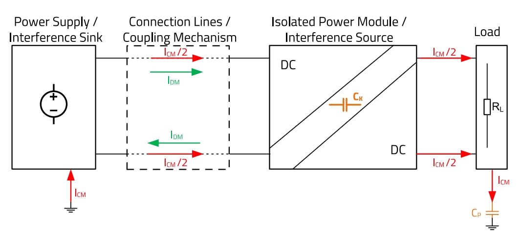
Figure 1: Basics of differential and common mode interference.
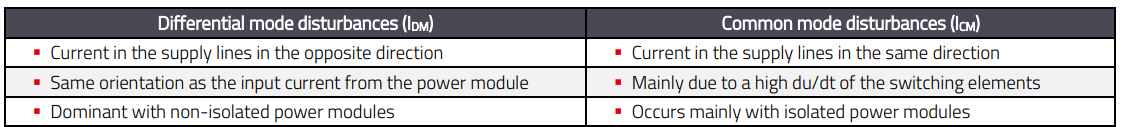
Table 1: Comparison of interference types.
2. MAGI³C POWER MODULE AND EMC ENVIRONMENT
Isolated power modules are used in many industrial applications. Be it as a supply for an RS485 interface or for sensor data acquisition. Due to the wide range of possible applications and the resulting different environmental conditions, i.e. different CP's, we use a standardised structure based on CISPR 16-2-1 to ensure that the filters can be compared with each other.
2.1 Test setup based on CISPR 16-2-1
Figure 2 illustrates the setup that forms the basis for the tests in this article.
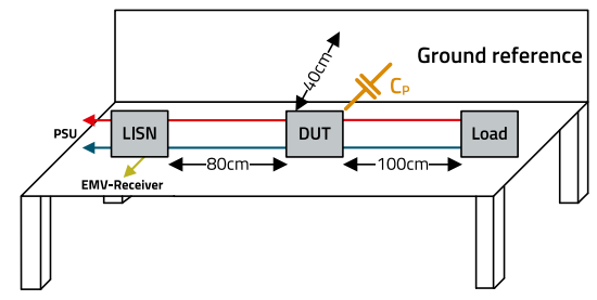
Figure 2: EMC test setup based on CISPR 16-2-1.
The setup shows the essential components that are necessary for a conducted measurement of the interference voltage. A detailed description of the measurement setup in accordance with CISPR 16-2-1 can be found in the Support Note SN023 | Conducted emissions test.
The device under test (DUT) is a MagI³C evaluation board with a size of 80 × 80 mm. The coupling capacitance (CP) in Figure 2 is representative of the
- parasitic capacities of the DUT for ground reference
- parasitic capacitance of the load to ground reference
- parasitic capacitance of the load lines to the ground reference
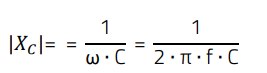
The coupling capacitance to the environment (ground reference) forms the path for the common mode current to close the circuit. However, the impedance of the capacitance is not a fixed value but varies with the frequency. This is clearly reflected in the formula for the capacitive reactance |XC|:
 (1)
(1)
ω – K Circular frequency [Hz]
C – Capacitance [F]
F – Frequency [Hz]
The following two subsections present methods for determining the value of the coupling capacitance CP. For clarification, the respective values are determined using a numerical example that corresponds to the structure used in this article. Both methods are approximations and cannot provide an exact value due to the complexity of the real structure of a coupling capacitance.
Figure 3 shows the structure and the power module (evaluation board) with the components that are relevant for the common mode analysis.
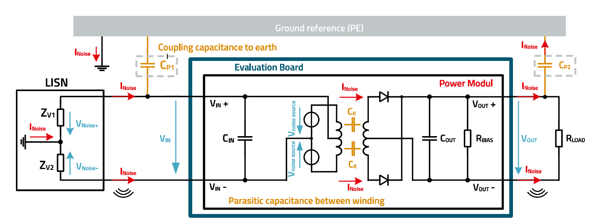
Figure 3: Schematic measurement setup based on CISPR-16-2-1.
The switching elements on the primary side of the power module are the source of the common mode interference. The switched voltage Vnoise drives a current INOISE through the intermediate winding capacitance CK of the transformer to the secondary side of the power module. The interference currents propagate via the output lines and flow via the coupling capacitance CP2 to the earth reference (PE). The circuit to the input of the evaluation board is then closed via the earth reference and CP1. The output and input lines also act as antennas, which leads to the ‘radiation’ of parts of the interference current INOISE.
2.2 The coupling capacitance CP to the environment - theoretical determination via the geometry
The areas and geometries of different potentials and their distance from each other are decisive for the formation of a parasitic capacitance. In the case under consideration, the DUT consists of an evaluation board (EVB) with an area of 80 × 80 mm, whereby the insulated module used is operated with a resistive load. The output cables used to the load have a length of 100 cm and the distance to the measuring plate (ground reference) is 40 cm. Two cases must therefore be considered when determining the coupling capacitance CP. Case 1, the coupling of the evaluation board to the measuring plate and Case 2, the coupling of the output lines to the measuring plate, as shown in Figure 3.
This allows us to use the two cases shown in Figure 3 and calculated in Figure 4 as a basis for determining the coupling capacitance. The influence of the ohmic load, in this case represented by a sliding resistor, was not taken into account.
2.3 The coupling capacitance CP to the environment - metrological determination via the resonance
A metrological approach is to connect a defined inductance in series with the coupling capacitance to the environment and thus create a series resonant circuit. The required CP can then be calculated using the frequency at resonance and the formula for the series resonant circuit.
The size of the inductance inserted is determined by the existing inductance values such as transformer, cables, copper tracks etc. For the power module we are looking at here, we have inserted a PD2 inductance of 15 µH into both the positive and negative lines of the power module input. It is important here not to select an inductance value that is too high, as otherwise the inductance would influence the power module and therefore no measurement would take place during normal operation. On the other hand, the inductance must be large enough in relation to the line inductances so that these can be neglected in the analysis.
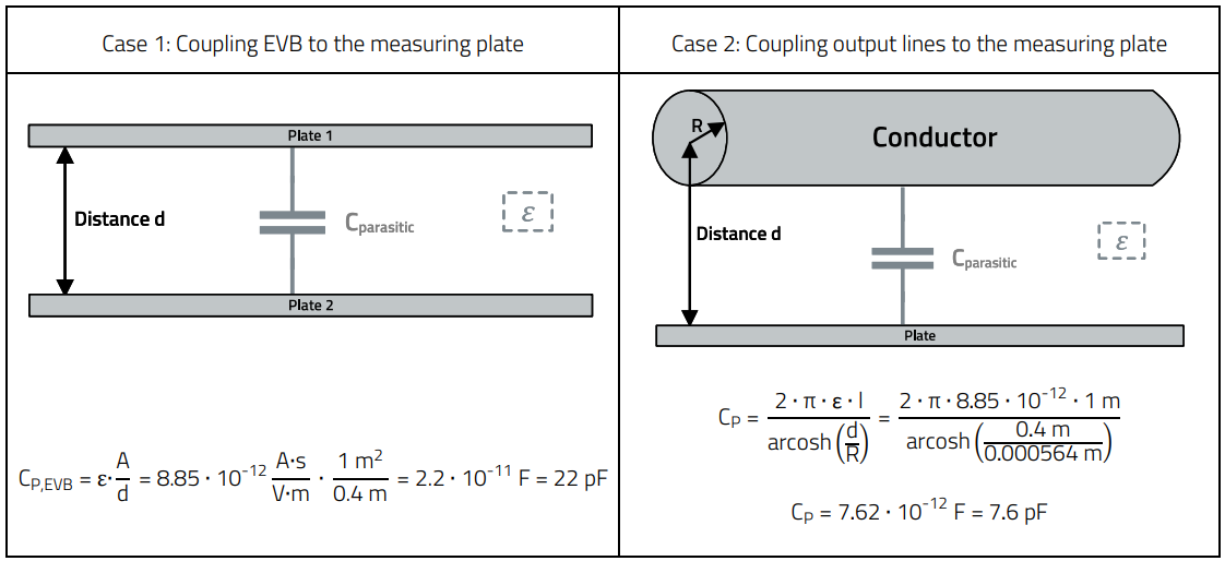
Figure 4: Examples of coupling capacities.
Analysing the measurements in Figure 5 shows that there is a resonance point at approx. 15 MHz.
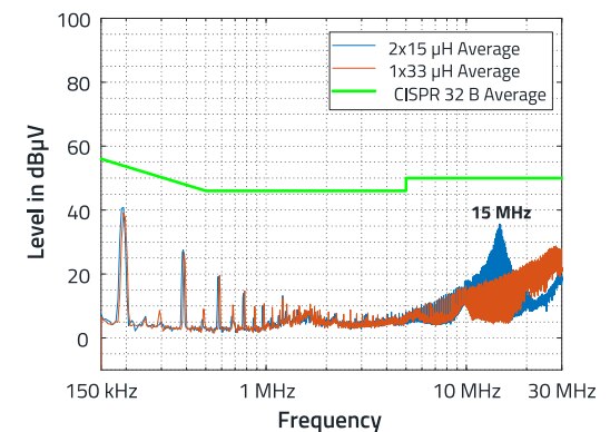
Figure 5: EMC plot with resonance point of the conducted interference voltage.
The value of the parasitic capacitance can be calculated using the resonance frequency and the inserted inductance. Due to the output capacitance, both output lines are at the same potential in the high-frequency range so that they can be considered together as a single line for the calculation. The total inductance L corresponds to the parallel connection of the two 15 µH inductors introduced, resulting in a value of 7.5 µH for the calculation of the parasitic capacitance.
The formula for the series resonant circuit, converted to CP, provides the required value:
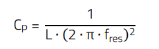 (2)
(2)
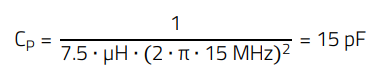 (3)
(3)
The first estimate of the CP with 22pF based purely on the geometric view, see Figure 4: Case 1, is therefore sufficiently accurate. The deviation from the value determined by measurement is due to the influence of the load and the structure itself.
3. COMMON MODE INTERFERENCE SUPPRESSION WITH BRIDGE CAPACITOR
3.1 The intention of filtering
The most elegant way to pass the EMC test is to prevent interference, in this case common mode interference, from reaching the network simulator (LISN) in the first place. For an isolated power module, this means that the interference current is diverted past the LISN. But what does this mean for the case under consideration here? Figure 6 is a simplified representation of the real set-up as already shown in Figure 3. The figure illustrates the fundamentals on which the derivation of the equation is based.
Figure 6 shows both (path 1 & path 2) interference current loops. Path 2, marked in red, illustrates the path of the common mode interference current that flows through the power module via CK and closes its circuit via earth.
Path 1, marked in blue here, shows an alternative loop. The current flows through the power module and then makes anb ‘arc around the power module’. The interference current thus flows past the LISN.
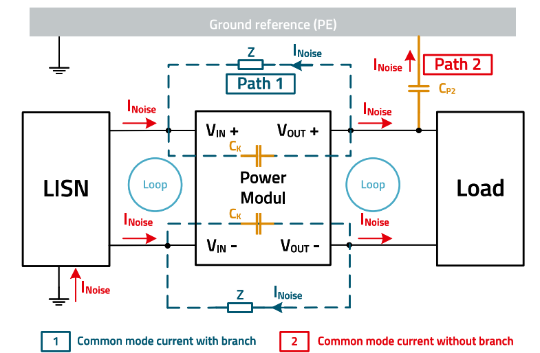
Figure 6: Equivalent circuit diagram with representation of the interference currents
To summarise, this means:
- Interference current circulates within the power module and cannot flow into the surrounding system.
- No interference current through the LISN means no interference potential at the LISN.
But why should the interference current choose the branch?
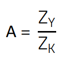
Path 1 must be more ‘attractive’ for INOISE than path 2, i.e. it must have a lower impedance than path 2. This means that only a capacitor can be considered as a component, see Formula 1.
Path 1 is therefore the resulting interference loop in and around the power module.
The equivalent circuit diagram can now be extended by a real component for the branch as follows.
The equivalent circuit diagram shown in Figure 7 has already been expanded to include the required elements, as it forms the basis for the subsequent determination of the equations.
The input and output capacitances of the power module, shown in grey, balance, i.e. distribute the common mode interference currents so that only one CY is required instead of two.
3.2 EMC meets Kirchhoff's law
In order to determine the efficiency of the measure with the Y-capacitor, the circuit without the junction should be compared with the circuit with the implemented junction. In other words, we compare the voltage drop of the interference current at the LISN with bridge capacitor with the voltage drop without bridge capacitor. The ratio, expressed in dB, is then the attenuation a (Figure 8).
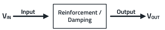
Figure 7: Basic concept for calculating damping.
In this case, the configuration without Y capacitor (amplitude A1) is compared with the configuration with Y capacitor (amplitude A2):
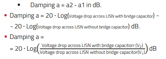
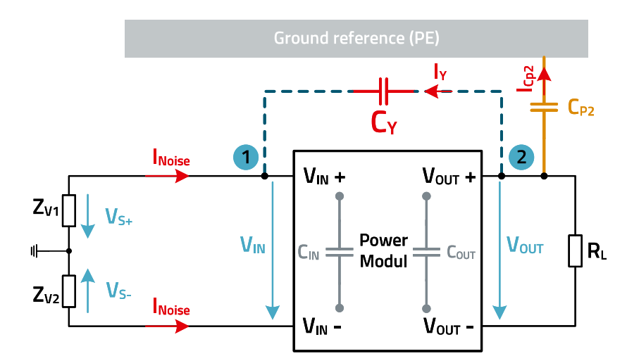
Figure 8: Equivalent circuit diagram with capacitive branching of the common-mode fault.
For the further calculation, the factor A is introduced, which represents the ratio of ‘voltage drop at the LISN with bridge capacitor’ to ‘voltage drop at the LISN without bridge capacitor’.
 (4)
(4)
To determine the value of the bridge capacitor, we must now convert the known circuit diagram into a simplified electrical equivalent circuit diagram, to which we can then apply Kirchhoff's law. Kirchhoff's law consists of two basic rules: The node rule (1st Kirchhoff's law) states that in a node the sum of the incoming currents is equal to the sum of the outgoing currents. The mesh rule (2nd Kirchhoff's law) states that the sum of the voltages in a closed loop is equal to zero (Figure 9 and Figure 10).
A simplified equivalent circuit diagram can be created from the illustrations. Here, the supply lines to the power module are simplified to a single line corresponding to the parallel connection. ZV represents the two impedances ZV1 and ZV2 of the LISN. The impedance of the parasitic coupling capacitance between the primary and secondary side of the transformer in the power module is the impedance ZK. The capacitance CP2 represents the total parasitic capacitance on the secondary side and applies equally to both lines. VS represents all common mode interference voltage sources in the power module, see figure 3 Vnoise source. ZY is the impedance of the bridge capacitor that connects VOUT+ to VIN + and is parallel to the impedance ZK.
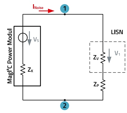
Figure 9: Equivalent circuit diagram, voltage drop without bridge capacitor.
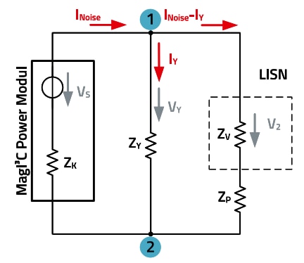
Figure 10: Equivalent circuit diagram, voltage drop with a bridge capacitor of impedance ZY.
Voltage drop without bridge capacitor:
The LISN, the parasitic capacitance and the MagI³C power module are connected in series here. We can therefore calculate V1 using the familiar formula for a voltage divider. If we now rearrange the basic equation for the series connection according to the voltage V1 we are looking for, we obtain the following equation, which represents the voltage drop across the LISN.
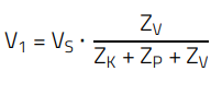 (5)
(5)
V1, V2 – Voltage drop across the LISN
ZK – Impedance of the winding capacitance
ZP – Impedance of the parasitic coupling capacitance
ZV – Impedance of the LISN
VY – Voltage drop across the bridge capacitor
ZY – Impedance of the bridge capacitor
VS- Common-mode interference voltage source
Voltage drop with bridge capacitor:
In the following, the circuit is a mixture of a series and a parallel circuit. ZY, the bridge capacitor, is connected in parallel with the LISN and the parasitic capacitance. The parallel branch is then connected in series with the MagI³C power module.
If we now rearrange the basic equation for the parallel circuit and the series circuit according to the voltage V2 we are looking for, we obtain the equation that represents the voltage drop across the LISN when the bridge capacitor is implemented.
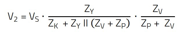 (6)
(6)
V1, V2 – Voltage drop across the LISN
ZP – Impedance of the parasitic coupling capacitance
ZV – Impedance of the LISN
VY – Voltage drop across the bridge capacitor
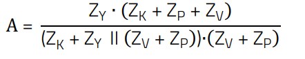
If we now insert the equation for V1 and V2 into the damping equation, we obtain the required expression.
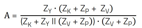 (7)
(7)
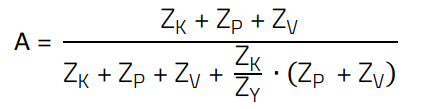
This equation can be further simplified for our purposes. Chapter 5.1 shows the exact derivation for the simplification and the expected error using a numerical example.
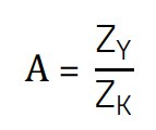 (8)
(8)
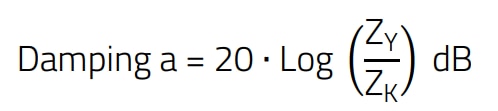 (9)
(9)
4. PRACTICAL EXAMPLE WITH A REAL MAGI³C POWER MODULE
To illustrate the rule of thumb, a sample calculation is carried out step by step based on the interference voltage result of an SIP-4 Power Module. The electrical characteristics are: VIN = 12 V, VOUT = 5 V, IOT = 200 mA (Order Code: 177920521).
Figure 11 shows the result of the interference voltage measurement.
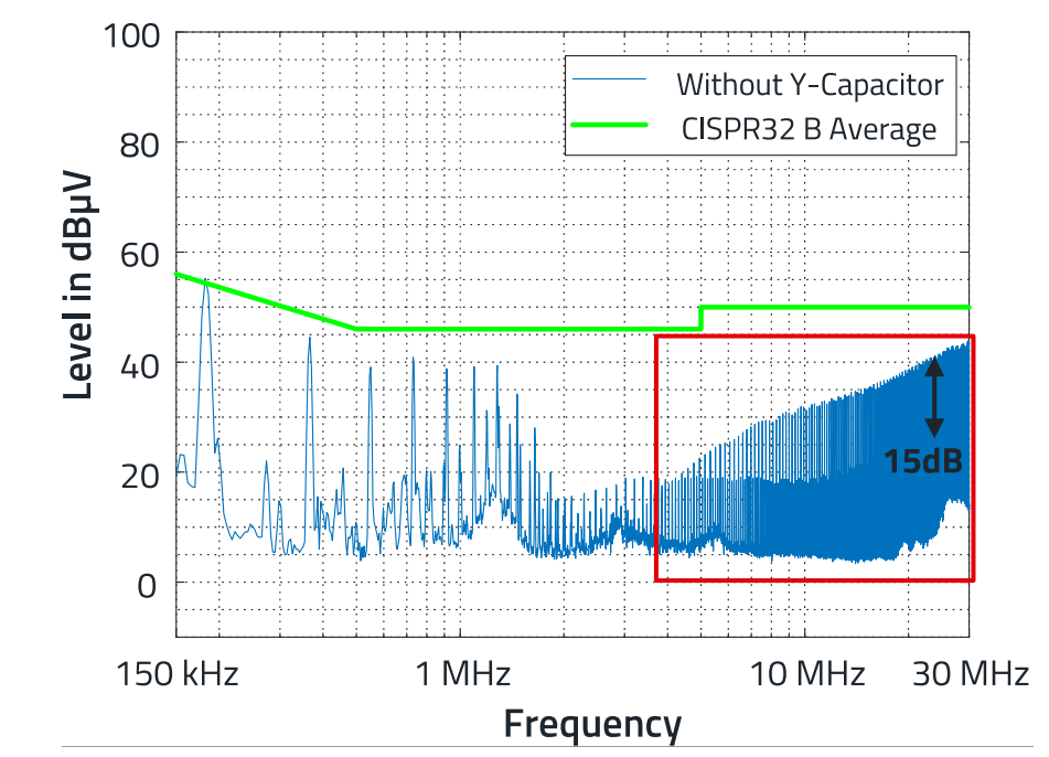
Figure 11: Interference voltage protocol, SIP-4 power module.
The calculation is based on a current clamp measurement; the frequency range considered here for the common mode interference is between 4 MHz and 30 MHz. In the frequency range below 4 MHz, the interference voltage is determined by the differential mode interference. Figure 11 shows that in the frequency range around 30 MHz, the distance of the interference voltage to the limit value according to CISPR 32 is approx. 12 dBµV.
The further design is based on an attenuation of 15dB in the 20 to 30MHz range, see Figure 11.
Step 1: Determination of the desired attenuation in the frequency range from 4 MHz to 30 MHz.
Step 2: Determine the coupling capacitance between the windings of the Power Module's transformer. The value for the coupling capacitance between the windings can be found in the data sheet of the power module. The value is usually specified as a maximum value, i.e. as a worst-case value. For the SIP-4 power module, 75 pF is specified for CISO, i.e. for CK.
The value for CISO is typically determined at a measurement frequency of 100 kHz. For our calculation, however, CK can be regarded as stable up to 30 MHz.
Step 3: Calculation of the value for the bridge capacitor, based on the simplified equation.
 (10)
(10)
Conversion from the required attenuation of 15 dBV logarithmic to a linear value.
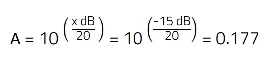 (11)
(11)
This results in a bridge capacitor value of:
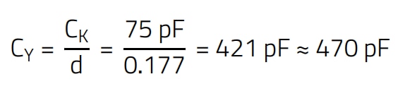 (12)
(12)
The value CY = 470 pF was chosen because it corresponds to a discrete component value.
Step 4: Verification of the value for the bridge capacitor using a real conducted EMC measurement, the result is shown in Figure 12.
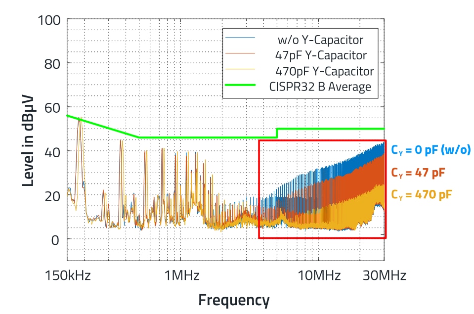
Figure 12: Measurement of conducted interference voltage with various bridge capacitors.
The greater the capacitance of the bridge capacitor, the higher the resulting attenuation in the frequency range above 3 MHz, as the path for the interference current has a lower impedance. It can also be seen that the attenuation with the real capacitance is higher than the calculated value. The calculation resulted in an attenuation of 17.2 dB for a bridge capacitor with a capacitance of 470 pF. However, the measurement shows an attenuation of almost 19 dB. This is a difference of 2 dB, which is due to the parasitic coupling capacitance CK of the transformer, which changes the actual attenuation. The data sheet only specifies a maximum value. In practice, however, the coupling capacitance between the windings of the transformer is less than 75 pF, it is only 60 pF.
However, the deviation between the calculated and measured value can also be due to the measurement uncertainty, simplifications in the model and component tolerances.
5. LIMITS OF THE RULE OF THUMB & CONCLUSION
The bridge capacitor acts as a low-impedance bypass and minimises the interference current to the network simulation (LISN). However, due to its properties as a frequency-dependent impedance, the capacitor cannot ‘keep out’ the interference current over the entire frequency spectrum of the measuring range of the conducted interference voltage. The counterpart to the bridge capacitor is the coupling capacitance CP to the environment. It is significantly influenced by the distance between the structure and the earth plate, but also by the length of the output lines. The bridge capacitor can only effectively divert the interference current if its capacitance is much greater than that of the coupling capacitance to the environment.
5.1 Validity of the simplification
The limits of the simplification are explained using a numerical example. The following values are selected for the variables involved in the example:
Parasitic coupling capacity to the environment CP:
CP = 20 pF→ZP=795 Ω @ 10 MHz.
Bridging capacitor CY:
CY = 470 pF → ZY=34 Ω @ 10 MHz
Parasitic winding capacitance CK:
CK = 75 pF → ZK=212 Ω @ 10 MHz
Impedance of LISN ZV:
ZV = 25 Ω
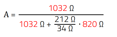
The equation for the required attenuation α then becomes:
 (13)
(13)
 (14)
(14)
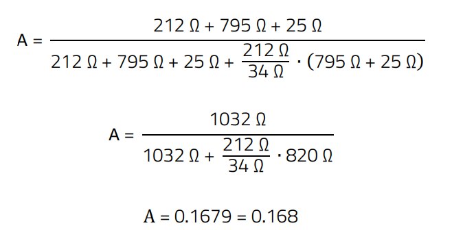 (15)
(15)
It is noticeable in the equation that the numerator and denominator values are close to each other. These are marked in red to make them easier to read.
 (16)
(16)
The values marked in red are all approx. 1000. If we now replace the values with 1000, the equation can be simplified as follows.
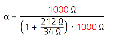 (17)
(17)
The 1 in the bracket in the denominator can be deleted as it is more than 6 times lower than 212 Ω/24 Ω
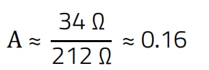 (18)
(18)
If the results of the two variants of the formula are compared, the following difference emerges: see Table 2.

Table 2: Comparison of both variants of the formula.
The following illustration (Figure 13) serves to better assess this effect or situation:
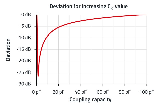
Figure 13: A Deviation as a function of the parasitic coupling capacitance CP and the parasitic winding capacitance CK.
The graph clearly shows that the error in applying the ‘short formula’ increases the closer the coupling capacitance CK of the transformer is to the determined value of the parasitic coupling capacitance CP.
5.2 Conclusion
The great effect of a bridge capacitor in reducing the common mode interference voltage was proven by measurement. The measurements have also clearly shown that the theoretical approach using the formula determined is a good way to determine a starting value for a bridge capacitor. The formula can always be used in its long form as it has no simplification based on the ratios between CP and CK. Only when using the short formula must attention be paid to the ratio between CP and CK as it has an essential influence on the effectiveness of the formula.
IMPORTANT NOTICE
The Application Note is based on our knowledge and experience of typical requirements concerning these areas. It serves as general guidance and should not be construed as a commitment for the suitability for customer applications by Würth Elektronik eiSos GmbH & Co. KG. The information in the Application Note is subject to change without notice. This document and parts thereof must not be reproduced or copied without written permission, and contents thereof must not be imparted to a third party nor be used for any unauthorized purpose. Würth Elektronik eiSos GmbH & Co. KG and its subsidiaries and affiliates (WE) are not liable for application assistance of any kind. Customers may use WE’s assistance and product recommendations for their applications and design. The responsibility for the applicability and use of WE Products in a particular customer design is always solely within the authority of the customer. Due to this fact it is up to the customer to evaluate and investigate, where appropriate, and decide whether the device with the specific product characteristics described in the product specification is valid and suitable for the respective customer application or not. The technical specifications are stated in the current data sheet of the products. Therefore the customers shall use the data sheets and are cautioned to verify that data sheets are current. The current data sheets can be downloaded at www.we-online.com. Customers shall strictly observe any product-specific notes, cautions and warnings. WE reserves the right to make corrections, modifications, enhancements, improvements, and other changes to its products and services. WE DOES NOT WARRANT OR REPRESENT THAT ANY LICENSE, EITHER EXPRESS OR IMPLIED, IS GRANTED UNDER ANY PATENT RIGHT, COPYRIGHT, MASK WORK RIGHT, OR OTHER INTELLECTUAL PROPERTY RIGHT RELATING TO ANY COMBINATION, MACHINE, OR PROCESS IN WHICH WE PRODUCTS OR SERVICES ARE USED. INFORMATION PUBLISHED BY WE REGARDING THIRD-PARTY PRODUCTS OR SERVICES DOES NOT CONSTITUTE A LICENSE FROM WE TO USE SUCH PRODUCTS OR SERVICES OR A WARRANTY OR ENDORSEMENT THEREOF. WE products are not authorized for use in safety-critical applications, or where a failure of the product is reasonably expected to cause severe personal injury or death. Moreover, WE products are neither designed nor intended for use in areas such as military, aerospace, aviation, nuclear control, submarine, transportation (automotive control, train control, ship control), transportation signal, disaster prevention, medical, public information network etc. Customers shall inform WE about the intent of such usage before design-in stage. In certain customer applications requiring a very high level of safety and in which the malfunction or failure of an electronic component could endanger human life or health, customers must ensure that they have all necessary expertise in the safety and regulatory ramifications of their applications. Customers acknowledge and agree that they are solely responsible for all legal, regulatory and safety-related requirements concerning their products and any use of WE products in such safety-critical applications, notwithstanding any applicationsrelated information or support that may be provided by WE. CUSTOMERS SHALL INDEMNIFY WE AGAINST ANY DAMAGES ARISING OUT OF THE USE OF WE PRODUCTS IN SUCH SAFETYCRITICAL APPLICATION.
DIRECT LINK
ANS022 | Bridge capacitor for isolated power modules, the whole truth, no myths
USEFUL LINKS:
Application Notes : https://we-online.com/en/support/knowledge/application-notes
Services: https://we-online.com/en/products/components/service
Contact : https://we-online.com/en/support/contact
CONTACT INFORMATION
Würth Elektronik eiSos GmbH & Co. KG
Max-Eyth-Str. 1, 74638 Waldenburg, Germany
Tel.: +49 (0) 7942 / 945 – 0
Email: appnotes@we-online.de
