REFERENCE DESIGN
“GB PoE+ - Ethernet-USB” adapter for industrial use with an EMC perspective
RD022 BY Dr. Heinz Zenkner
01. INTRODUCTION
The “GB PoE+ - Ethernet-USB” adapter was developed on the basis of the reference design “GB-Ethernet-USB Adapter”, which operates without Power over Ethernet (PoE). The adapter without PoE is described in detail in Application Note RD016; the electromagnetic compatibility tests can be found in Application Note ANP116. The “GB PoE+ - Ethernet-USB” adapter has three interfaces, one USB Type-C (USB 3.1), one RJ45/Ethernet 1 Gigabit interface with integrated Power-over-Ethernet (PoE+) supply, and one terminal to the DC/DC converter with an adjustable output voltage of 6 - 18 V and a maximum output power of 25 W. The board was developed to familiarize users with PoE technology. As with the design without PoE, the bit error rate and transmission speed can be investigated using a Windows application. In addition, the user also has an optimized circuit design and layout, for both the USB 3.1 and the GB-PoE Ethernet interface.
02. THE INTERFACE
2.1 Gigabit Power over Ethernet (PoE) interface – technology, signals
The aspects of signal transmission, data rate, bandwidth and error correction at 1000BASE-T are described in Application Note RD016. This is complemented here with a detailed explanation on the “Power over Ethernet” power supply. Power over Ethernet (PoE) is generally specified for systems with a maximum supply voltage of 57 VDC and consumer-side power up to 73 W. At the moment of switch-on, the voltage is > 42 V. In normal operation, it is in the range of 36 to 57 V. However, there are different power classes, which are also designated or abbreviated differently:
- IEEE 802.3af (PoE) provides 15 W output power or up to 12.95 W at the terminal device.
- IEEE 802.3at (PoE+) provides 30 W output power or up to 25.5 W at the terminal device.
- IEEE 802.3bt (4PPoE) provides 90 W output power or up to 71.3 W at the terminal device.
- IEEE 802.3bu (PoDL) for single-pair Ethernet

Table 1: Overview of the most important characteristic data of the Ethernet standards and the associated classes
PoE systems encompass Power Sourcing Equipment (PSE) and the Powered Device (PD, load) and have a recommended maximum cable length of 100 m. Due to the small conductor cross-sections, long cable lengths and low system voltage, there is significant power loss in the cable, which can lead to a poor system efficiency. For example, at Class 4, 25.5 W can be drawn at the PD, at 100 m length the line can have up to 12.5 Ω loop resistance, and a maximum current of 600 mA is permitted. This results in up to 4.5 W power loss in the cable, which equates to an efficiency of just 82%! PoE is specified in the IEEE 802.3af-2003 standards (Section 33 in IEEE 802.3-2005) or the 2009 update, IEEE 802.3at. Different power supply techniques are used depending on the system.
- Phantom power supply: Power transmission is via the signal-carrying wire pairs.
- Spare-pair power supply Power transmission is via the unused wire pairs.
In conventional 10BASE-T and 100BASE-TX Ethernet, only two of the four wire pairs are used for data transmission. The other two free wire pairs can be used for PoE (power). Data is transmitted via one path, power via the other, which corresponds to “spare pair power supply”. When PoE was first introduced, it was the safest way (Table 2 above), to transmit data and power simultaneously via one cable.
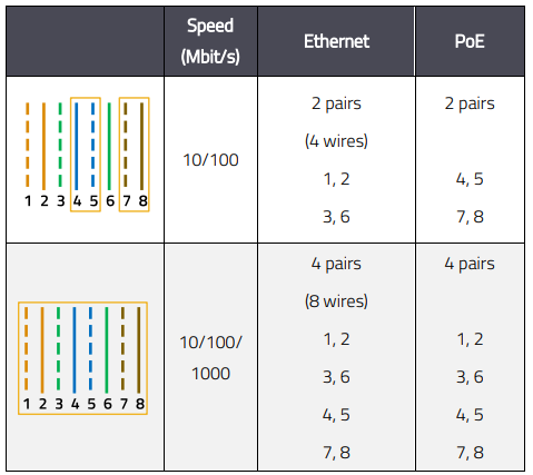
Table 2: Wire configuration in the Ethernet cable for 10BASE-T, 100BASE-TX and 1000BASE-T (Gigabit Ethernet)
In the case of 1000BASE-T (Gigabit Ethernet), all four pairs are used for data transmission. Here, the data and power are transmitted via the same wire pairs (Table 2 below), so this corresponds to the “phantom power supply”. This method is possible here, because with Ethernet over twisted pair cables, differential data transmission takes place over each pair with decoupling via a transformer. The signal transmission itself does not differ from transmission without PoE; the data rates and signal amplitudes are the same.

Table 3: Power-up sequence with the associated voltage ranges
2.2 Gigabit Ethernet interface with PoE interface structure
The “GB PoE+ - Ethernet-USB” adapter works according to the IEEE 802.3at standard (PoE+) with up to 25.5 W at the PD. Figure 1 shows the basic circuit of a PoE+ system.
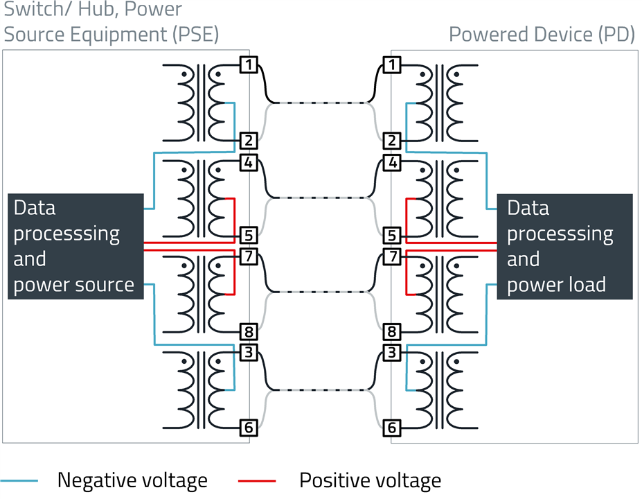
Figure 1: Basic circuit of a system according to IEEE 802.3at or PoE+
The DC supply and load connections can be taken from the center taps of the transformers on both the PSE and PD sides. Each wire pair operates in common mode through the center taps as one side of the DC power supply (plus or minus), so two pairs are required to complete the circuit. The polarity of the DC supply is not important, as rectification is provided on the PD side. The powered device must be operated with one of the two pairs: Spare pairs 4-5 and 7-8 or data pairs 1-2 and 3-6.
2.3 Power-up process, PoE detection
Before the PSE (Power Sourcing Equipment) supplies power, it must first classify the terminal device. Damage to non-PoEcapable terminal devices is avoided this way and the power provided by the PSE is limited to the necessary power by classifying the PD (Powered Device) to limit damage. The power source of the PSE uses a classification current and a low voltage to determine whether the terminal device is PoE- capable at all and then which class it belongs to. Depending on the terminal device, an exchange of information (handshake procedure) is therefore necessary between the power source and the terminal device, whereby the terminal device communicates its PD class. In order to distinguish PoE-capable terminal devices from unsuitable ones in the first step, a process called "resistive power discovery" is used in the PoE power source. A PoEcapable terminal device has an input circuit with passive components for this purpose. The PSE current source checks the internal resistance of this PD circuit with a measuring circuit. If the resistance is between 19 kΩ and 26.5 kΩ and the line has a capacitance of ≤ 150 nF, the power supply is activated. In a second detection phase, the performance class is determined (Table 1). Here the PD is supplied with a rising voltage until it signals to which of the four performance classes defined in the 802.3af standard it belongs. The correct power is then supplied. This detection takes about one second in total. To prevent damage to terminal devices, the PSE automatically turns off power to the relevant port as soon as a PD is removed from the LAN. The power-up process is shown graphically in Figure 2, the power-up steps with the associated process and voltage range in Table 3.
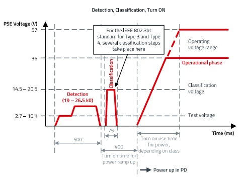
Figure 2: Power-up sequence for operation between PSE and PD
Table 4 shows the breakdown of the classes (classification according to Table 3) and the necessary loop current ranges between PSE and PD for detecting or assigning the classes. The gray lines, i.e., the intermediate values, are ignored by the classification system.
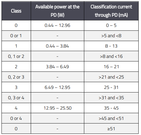
Table 4: Division of the classes (classification according to Table 3) and the associated necessary ranges of the loop currents between the PSE and PD; intermediate values are ignored; classification current = defined load resistance through PD
With 802.3bt (PoE++), two new PoE types (Type 3 and Type 4) and four additional classes were introduced in September 2018. The standard is completely backward compatible with previous PoE standards to work with older Type-1 and Type-2 devices without problems. The power output was increased to 90 W - 100 W at a current of 600 mA - 960 mA. All four wire pairs are required for the power supply in this case in order to limit losses on the lines. In order to keep the losses in the lines between PSE and PD low and also to achieve the high data rate, high demands are placed on the cables; an overview is shown in Table 5.

Table 3: Power-up sequence with the associated voltage ranges
03. HARDWARE DESIGN
3.1 Block diagram of the PD interface
Figure 3 shows the block diagram of the PD interface, one of four channels is shown. As far as the signal is concerned, the circuit is identical to the interface without PoE. In order to realize the power supply via the Ethernet cable to power the device at the same time, some extensions to the circuitry have to be implemented. Another common-mode choke is added to the PHY (Ethernet physical layer). This choke decouples the PHY-HF. Interference going from the cable to the interface is in common mode on the secondary side of the transformer. When operating with PoE, the DC/DC converter generates additional interference that can impair data transmission. The CM2 choke in Figure 3 reduces this interference. The CM1 and CM2 chokes are trifilar wound; i.e., all three windings are on a common core to attenuate common-mode interference. On the primary side to the cable, the center tap of the transformer to decouple the supply current and the Bob-Smith termination are also routed via the choke to decouple the power supply from the Ethernet cable.

Figure 3: Basic circuit of the GB-Ethernet interface with PoE: one of the four channels is shown

Table 5: Overview of the PoE standards, with associated power per port, the wire pairs used and the cable categories
The trifilar winding structure achieves magnetic field compensation, thus avoiding magnetization of the core by the supply current. On the secondary side, the trifilar structure of the CM 2 choke decouples the PHY in the high-frequency range (typically above 10 kHz). Figure 4 shows the insertion loss (S21) in common mode between J7/J8 (input at RJ45 jack) to D3 pins (output at D4+/CD4/D4-). Measurement was made at“1 Port RJ45 Through Hole 10/100/1000 Base-T, AutoMDIX, Power-over-Ethernet+ (PoE+) Module, WE-RJ45LAN HPLE, Order no: 7499511001A.
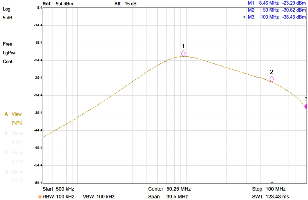
Figure 4: Insertion loss S21 up to 500 MHz, of a channel according to Figure 3 between input and output, measured with a network analyzer (impedance 50 Ω)
The insertion loss is at least 20 dB in the frequency range up to 100 MHz and can thus effectively attenuate interference typically in the frequency range between a few kHz and 50 MHz via the Ethernet cable. The measurement setup with spectrum analyzer is shown in Figure 5.
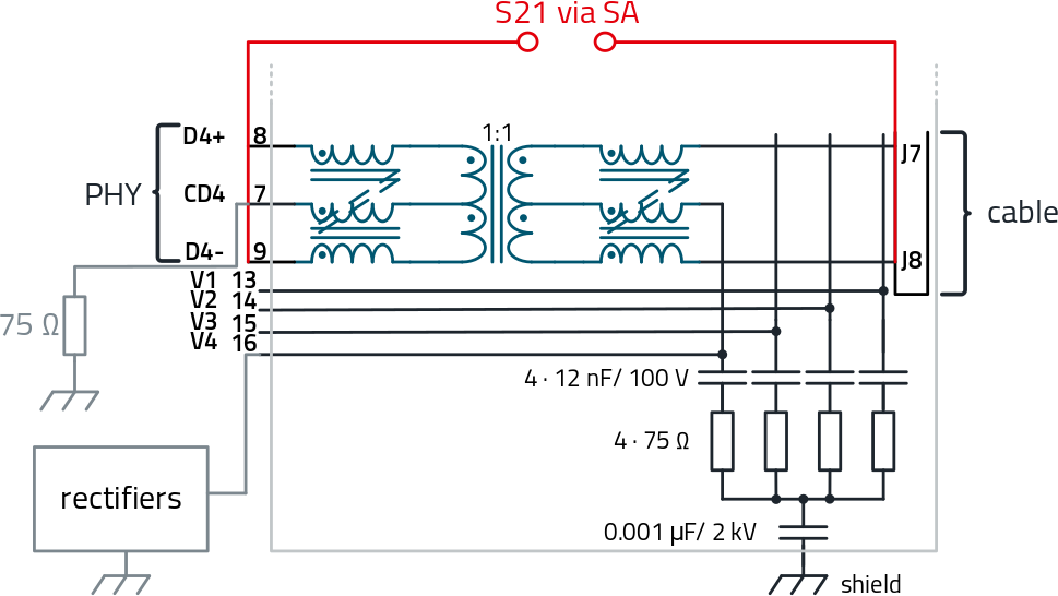
Figure 5: Measurement setup (schematic) for measuring the insertion loss S21 of a channel up to 100 MHz
3.2 Basic setup of the primary-side power supply
The power supply for the PD (Powered Device) is decoupled via the common mode chokes. The chokes prevent attenuation of the useful signal. In Figure 6 the basic circuit is shown.
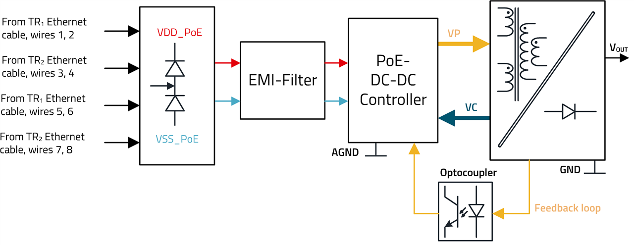
Figure 7: Basic circuit of the power supply (PoE)
The power supply for the controller electronics must meet the isolation requirements of IEEE 802.3-2005, Section 10, Reference 4. To meet this requirement, the secondary side “VOUT” of the power supply system must be isolated from the primary side (Ethernet cable) with a dielectric strength of at least 1500 VRMS. The unregulated voltage passes to the EMI filter, which attenuates high-frequency interference and includes additional transient protection. The PoE DC/DC controller regulates the input voltage (VDD/VSS), which is galvanically isolated via the transformer (Figure 7). After the rectifier, the regulated output voltage (VOUT) is available. The ground reference is isolated by a transformer; the ground reference is “AGND” on the primary side of the transformer and “GND” on the secondary side. Transformer no. 750311320 has a dielectric strength of 1,500 VRMS between the primary and secondary sides. The feedback loop for controlling the output voltage is galvanically isolated with an optocoupler. The optocoupler WL-OCPT, no. 140356145100 used here has an insulation dielectric strength of 3,750 VRMS. Figure 8 shows a schematic setup of the PCB with respect to the galvanically isolated areas.
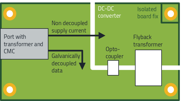
Figure 8: Schematic representation of the galvanically isolated areas on the PCB
04. DESIGN AND SETUP OF THE ADAPTER BOARD
The GB Ethernet USB adapter with PoE was developed as an “integrated variant”, so that in the area of the Ethernet interface, the matching network and the inductance block (consisting of common-mode chokes and transformers) are integrated into the RJ-45 jack housing (Figure 9).
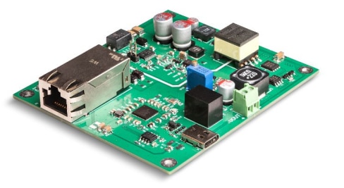
Figure 9: GB Ethernet USB adapter with PoE
4.1 Block circuit
The Gigabit Ethernet controller LAN7800 USB 3.1 connects the USB interface with the Ethernet interface, as a “bridge” (Figure 10). So the signal adaptation and decoupling have to be realized for switching the interfaces. The power supply must be decoupled via the Ethernet cable and regulated with a DC/DC controller. The DC/DC controller also handles the detection and classification of the power device (PD). On the USB side, a linear DC/DC controller (low drop regulator, LDO) generates the 3.3 V supply voltage required for the LAN7800 and the EEPROM. The LAN7800 requires an additional 4 kbit EEPROM for the firmware.
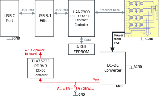
Figure 10: Block diagram of the GB-Ethernet-USB adapter with Power over Ethernet (PoE) circuit diagram, current flow in the adapter
4.2 Circuitry, current flow in the adapter
The circuit of the complete adapter is shown in Figure 11 and Figure 12. Figure 11 shows the USB and Ethernet interfaces with the PoE rectifier section, the LAN7800 controller and the small DC/DC controller for the 3.3 V supply voltage. The complete DC/DC converter is shown in Figure 12.

Figure 11: Circuit of the GB Ethernet adapter with PoE, signal section
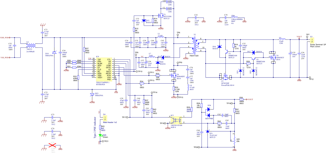
Figure 12: Circuit of the GB Ethernet adapter with PoE, DC/DC converter
4.3 USB-Ethernet controller
The LAN7800 is a high-performance USB 3.1 to GB-Ethernet controller with integrated Ethernet-PHY. An external 4 kbit EEPROM was connected for the onboard software. The circuit is shown in Figure 13. The upper part of the controller in the figure is the signal section, clocked with a 25-MHz quartz; the lower part is the controller’s relatively complex chip-internal power supply.
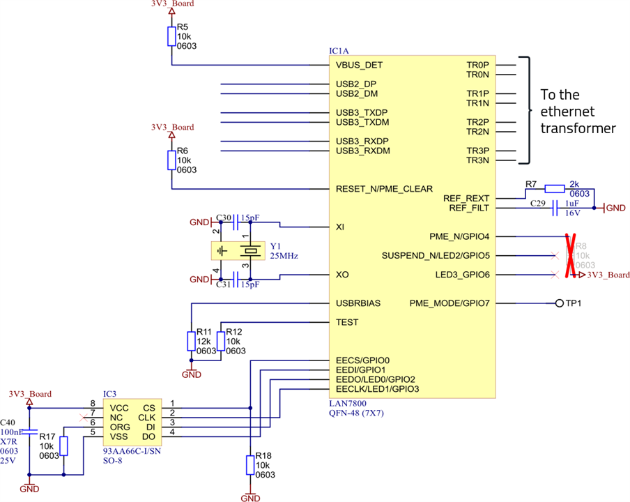
Figure 13a: Circuit of the controller: Signal section
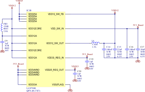
Figure 13b: Circuit of the controller: On-board power supply. L4: 74404032033, WE-LQS SMT semi-shielded storage choke, FB3: 742792625, WE-CBF SMT ferrite
4.4 USB 3.1 interface
The LAN7800 chip integrates a USB 3.1 SuperSpeed controller with USB-PHY. The circuit diagram of the USB 3.1 interface with associated signal filter is shown in. The power supply via the USB interface is not used here, because the supply is via the Ethernet interface (PoE).
The circuit of the USB interface is described in detail in Application Note RD016. The following is a summary.

Figure 14: Circuit diagram of the USB 3.1 interface
The data lines in the circuit diagram (Figure 14) are connected with current-compensated chokes with TVS Diode arrays against transient overvoltages. The PCB ground (GND) is connected to the GND terminals of the cable at component X1, but the connection is made to the package via a capacitor (C19) and a resistor (R1). If the capacitor C19 is fitted, the connection between GND and the package/shielding connection is also high-frequency and low-impedance. If the circuit is installed in a metal package, it may be advantageous for improving EMC (emission and immunity) to fit an SMD ferrite (e.g., 742792642) instead of C19. R1 is then omitted. The connection remains galvanic via the package and the PCB mounting holes.
The selection of filter components for the USB 3.1 signals is critical. The following components were selected for the circuit according to Figure 14:
- L2, L3: WE-CNSW-HF current-compensated SMT line filter (high frequency), 7442335600
- L5: WE-CNSW current-compensated SMT line filter, 744232090
- D2, D3, D4: WE-TVS TVS-Diode - Super Speed, 824012823
- C7, C8: WCAP-CSGP ceramic capacitor 100 V, 885012207128
The current-compensated choke in the USB 3.1 data lines must not influence the useful signal if possible. The choke used here has a differential-mode impedance of approx. 10 Ω at 500 MHz, so the influence at the super-speed data rate is not too high yet. The common-mode impedance for interference signal attenuation is 60 Ω at 100 MHz and increases to 140 Ω at 1000 MHz.
For the USB 2.0 compatible signal pair, D- and D+, a common-mode choke with higher impedance was chosen. Choke L5, a WE-CNSW current-compensated SMT line filter, has a differential-mode impedance of 30 Ω at 500 MHz, at 100 MHz it is 100 Ω, and at 1000 MHz it is already 350 Ω. The TVS Diode array used is the “WE-TVS TVS Diode - Super Speed” array with no. 824012823.
The coupling capacitors C7 and C8 in Figure 14 should have a capacitance between 75 nF and 200 nF. It should also be ensured that these coupling capacitors have sufficient dielectric strength to drain any transmit overvoltages coming from the interface to the downstream TVS Diode array without causing damage.
The balanced USB signal traces have an impedance of 90 Ω (+/-15%). Typically, a trace width of 0.11 mm and spacing between trace pairs of 0.13 mm should be maintained. All USB 3.1 traces must be routed on one level of the board and be referenced to a continuous ground plane. Vias and acute angles should be avoided wherever possible. An SMD variant should be selected for the USB jack in order to be able to dispense with vias for the USB 3.1 signal lines. The layout for this area is shown in Figure 15.
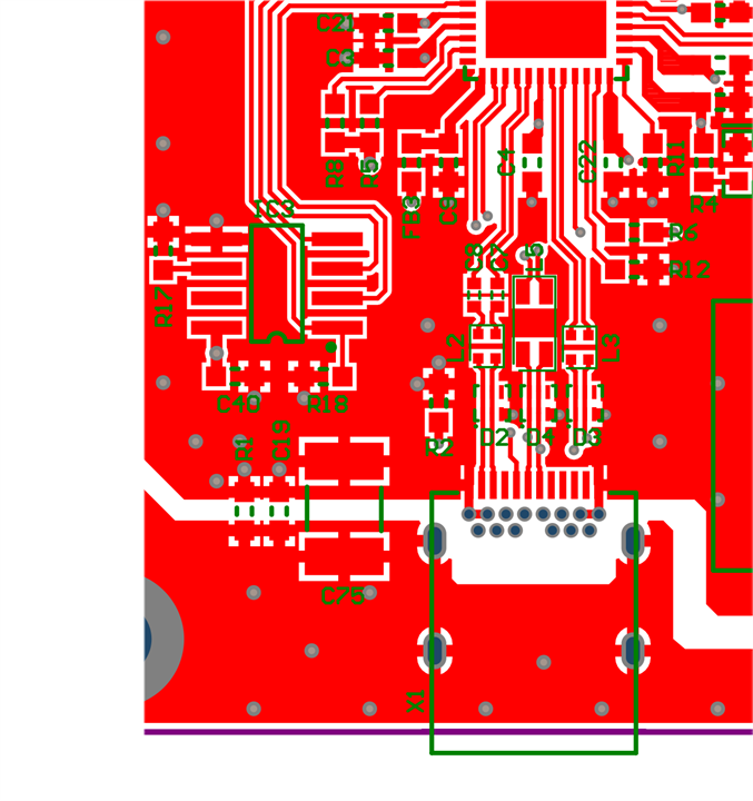
Figure 15: Layout, schematic representation of the USB 3.1 area.
4.5 Ethernet interface
The Ethernet jack includes the transformers, the input and output common-mode chokes, and the Bob-Smith terminations. Figure 16 shows part of the circuit diagram.
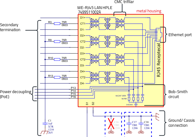
Figure 16: Part of the circuit diagram of the Ethernet front end
The transformer provides the functional galvanic isolation between the device and the cable; the required isolation voltage is 1,500 Vrms. On the primary side, impedance matching is achieved with the Bob-Smith network, on the secondary side with 75-Ω resistors. C1 provides galvanic isolation to prevent equalizing currents between devices. On the primary side, the supply voltage is decoupled via the center taps of the transformers. The Ethernet module is connected to “ground” via the S1 and S2 solder connections. Depending on the ground concept, this connection can be directly to a metal package or to the PCB ground (GND). For a detailed explanation, please refer to Application Notes RD016 and ANP116. The layout of the Ethernet interface area is shown in Figure 17.
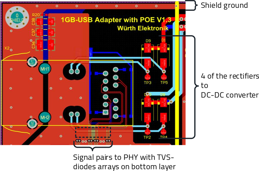
Figure 17: Layout of the area around the Ethernet interface
Package/socket ground to the electronics GND is isolated in all four layers, the areas of the package ground do not overlap with other layers. The ground planes are connected to each other with vias with a pitch of approx. 4 mm. The Ethernet signal pairs have a trace width of 0.154 mm and are spaced 0.125 mm apart. The TVS arrays must be connected directly into the signal path and to GND so as to avoid a voltage drop due to parasitic inductance. That is the reason why two arrays were used here, which are not fully connected. An extract of the circuit diagram is shown in Figure 18.
Figure 19 shows the layout extract and component placement.
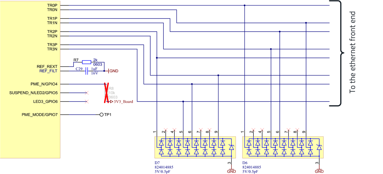
Figure 18: Circuit diagram excerpt of the Ethernet signal feed with the TVS Diode arrays WE-TVS TVS Diode - Super Speed series, no. 824014885
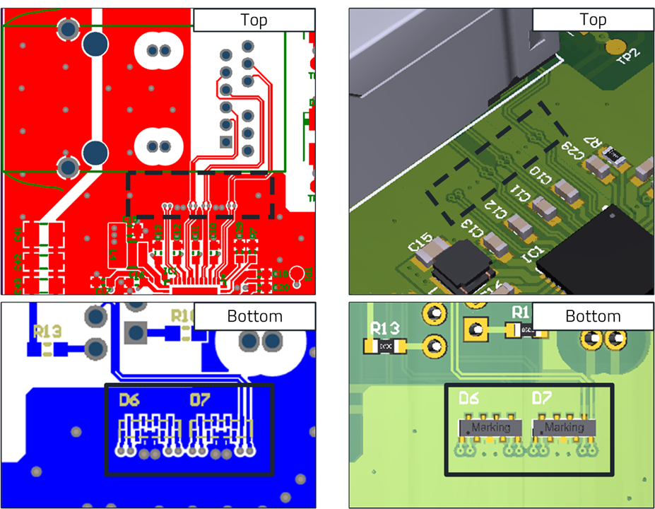
Figure 19: Layout extract and component placement of the signal path between the Ethernet front end and PHY
4.6 Power supply, Power-over-Ethernet (PoE)
The power supply part of the board is constructed on the basis of the TPS23754EVM-383 evaluation module from Texas Instruments. The circuit is shown in Figure 20.
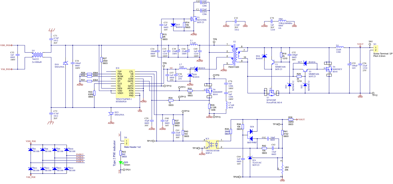
Figure 20: Circuit of the PoE power supply part
The TPS23754 controller IC is an IEEE 802.3at compliant PD and power supply controller. The isolated push-pull converter has a maximum output power of 25 W. The circuit features an active snubber (T1) and a synchronous rectifier (T3, 4, 5, 7). The galvanic isolation required by the standard is provided by T2 (transformer, no. 750311320) and IC5 (optocoupler, WL-OCPT no. 140356145100). The output voltage at X3 can be adjusted between 6 V and 18 V using the trimming resistor VR1. The supply voltage comes from the Ethernet cable pairs, decoupled via the transformer center taps and the trifilar common-mode chokes (Figure 16) and reaches the 8 Diodes (Figure 20 bottom left). The Diodes are then used to route the DC voltage to the filter stage and the controller. The layout associated with the circuit is shown in Figure 21.
The green line in Figure 21 galvanically isolates the primary from the secondary power supply area. The gaps and leakage paths must be observed here, which comply with safety standards such as IEC 62368. The two areas are isolated by all four layers of the PCB with a copper layer / trace spacing of 1.5 mm. The required minimum spacing is determined according to the gaps and leakage paths specified in IEC 62368, which have to be selected dependent on
- the peak voltage, i.e., 1,500 Veff ≙ 2,120 Vpeak)
- insulation grade (“basic or supplementary insulation”)
- degree of contamination, as applicable
Should higher insulation requirements be necessary due to the application, the components and the isolation spacing must be adapted accordingly!
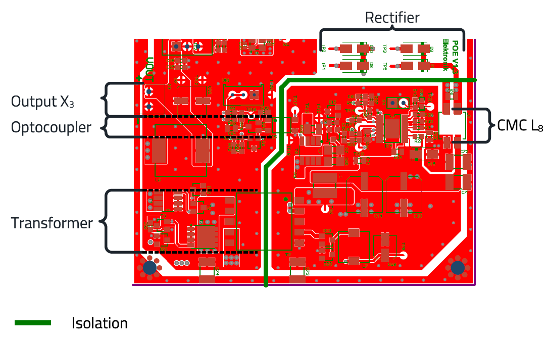
Figure 21: Layout of the PoE power supply part of the circuit according to Figure 19
Figure 22 shows the positions of the “EMC components”. On the top of the board there are component placement locations that can connect the “digital ground” (GND) to the package / shield ground. According to the circuit diagram in Figure 23, the components are C36, C37, C38, C41, C42, C43, C73, C74, R1, C19, C75.

Figure 22: GB adapter, position of the “EMC components” on the top of the board. According to the circuit diagram, C36, C37, C38, C41, C42, C43, C73, C74, R1, C19, C75 in Figure 23
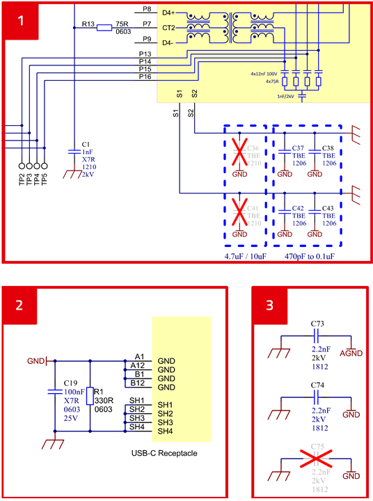
Figure 23: Excerpt from the circuit diagram of the “EMC components” on the top of the board according to Figure 22
The capacitors and the resistor are viewed as “component placement locations”, which can alternatively be assembled with capacitors, SMD varistors, 0-Ω resistors, or combinations. It is also possible to leave unassembled. For a detailed explanation, please refer to Application Note ANP116.
The underside of the assembly is shown in Figure 24, the corresponding “EMC components” are marked here too.
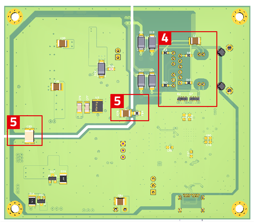
Figure 24: GB adapter, position of the “EMC components” on the underside
Figure 25 and Figure 26 show the excerpt from the circuit diagram for the components according to Figure 24. The 75-Ω resistors R3, R9, R10, and R13 with capacitor C1 (Figure 24) are the secondary side impedance termination to the PHY; the capacitor provides blocking for DC currents that may result from an offset of the PHY signal. The capacitor must have a dielectric strength of 2 kV. The D6 and D7 TVS Diode arrays protect the PHY from transient common-mode interference. The ground reference here is the PHY (GND)!
The capacitor C32 (Figure 25) connects the primary side ground (AGND) to the secondary side ground (GND) at the DC/DC converter. This capacitor provides a low-impedance return path for currents generated by the switching voltages between the primary and secondary windings of transformer T2. Without this low-impedance path, currents return from the secondary side to ground via stray capacitances, resulting in an increased conducted interference voltage. The rated voltage of the capacitor must be at least equal to the isolation voltage of the transformer. A capacitance of about 2200 pF is typically selected. C78 also capacitively connects AGND with GND. But here there is an additional SMD ferrite connected in series to attenuate an interference emission spectrum resonant in the range 20 to 30 MHz.
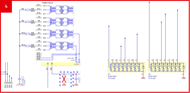
Figure 25: Excerpt from the circuit diagram, Part 1 the “EMC components” on the underside according to Figure 24
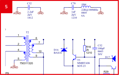
Figure 26: Excerpt from the circuit diagram, Part 2 the “EMC components” on the underside according to Figure 24
The SMD ferrite WE-CBF 742792021 has an impedance of approx. 4 Ω in this frequency range. This impedance does not affect the discharge of the interference current, but attenuates the resonance effectively.
In Figure 27, in addition to the active snubber (circuit around T1), an attenuated resonant circuit was connected between T6/Drain and T6/Source (AGND) using C76, C77 and L9. This circuit reduces an interference spectrum around approx. 23 MHz. The interference energy at MOSFET T6 is not high, so the transistor does not heat up noticeably, but the interference emission is still significantly reduced by about 6 dB. The excerpt from the circuit diagram and the corresponding position of the components on the PCB are shown in Figure 27.
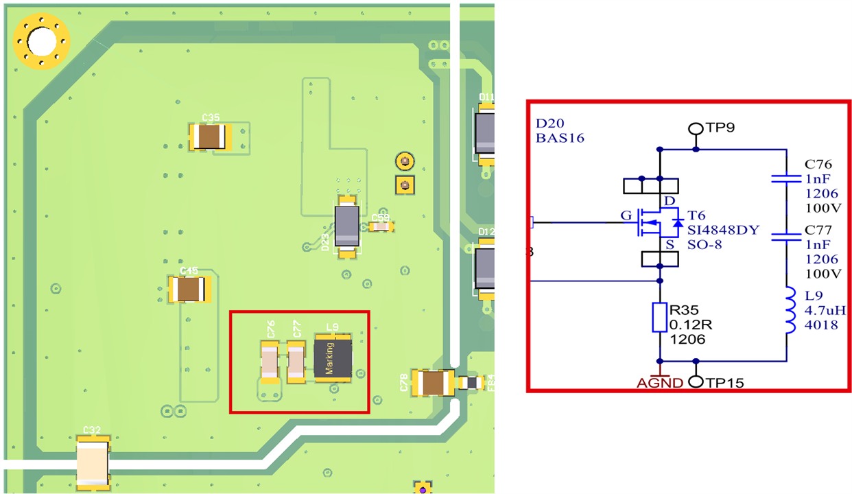
Figure 27: Passive resonance snubber at switching transistor T6. Circuit diagram and position on the PCB. L9: WE-LQS, 7440402047. C76, C77: WCAP-CSGBP 885012208106
To reduce common-mode interference, a highly effective filter was integrated between the DC/DC converter and the Diode array. Figure 28 shows the circuit diagram with the corresponding detail on the PCB. C53 and C54 reduce differential-mode interference, C71 and C72 reduce common-mode interference. The WE-SL2 common-mode choke with an inductance of 1 mH per winding is important here, however. The choke's pronounced resonant frequency is between 2 MHz and 8 MHz, yet the impedance is still 600 Ω at 100 MHz, which is sufficient for high filter insertion loss. By using a common-mode choke, current compensation is achieved in the power supply branch such that the ferrite core of the inductor does not go into magnetic saturation, thus keeping the impedance high and the component size small compared to having two separate inductors.
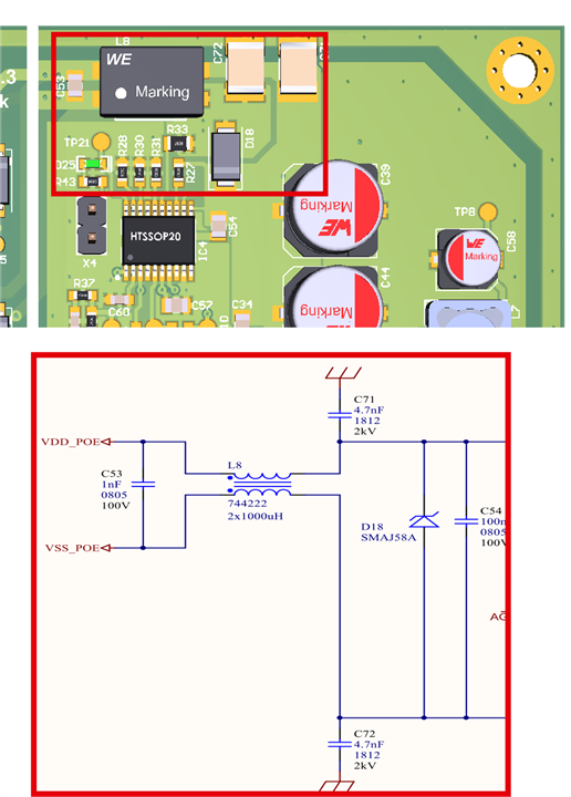
Figure 28: Filter between the DC/DC converter and rectifier, current flow and position on PCB
4.8 Software
The functions of the software are identical to those in the software on the board without PoE, so please refer to the description in document RD016.
4.9 EMC
The reference design was tested extensively in the company's own EMC lab. The results and a detailed description of the setup and interference suppression tips can be found in Application Note ANP122.
A Appendix
A.1 Bill of material
| Index | Description | Size | Electrical Properties | Part number |
| C1, C78 | Ceramic capacitor | 1210 | 1 nF, 2 kV, +/-10%, X7R | 885342209009 |
| C2, C65 | Ceramic capacitor | 1206 | 22 nF, 630 V, +/-10%, X7R | 885342208014 |
| C3, C4, C5, C6, C10 - C14 C16, C19, C21 - C24, C27, C28, C40 | Ceramic capacitor | 0603 | 100 nF, 25 V, +/-10%, X7R | 885012206071 |
| C7, C8 | Ceramic capacitor | 0402 | 100 nF, 25 V, +/-20 %, X5R | 885012105018 |
| C9, C18, C20, C29, C33, C60 | Ceramic capacitor | 0603 | 1 μF, 16 V, +/-10 %, X7R | 885012206052 |
| C15 | Ceramic capacitor | 0805 | 22 μF, 6.3V, +/-20 %, X5R | 885012107005 |
| C17, C26 | Ceramic capacitor | 0603 | 10 μF, 6.3 V, +/-20 %, X5R | 885012106006 |
| C25 | Ceramic capacitor | 0603 | 2.2 μF, 16 V, +/-20 %, X5R | 885012106018 |
| C30, C31 | Ceramic capacitor | 0402 | 15 pF, 50 V, +/-5 %, C0G | 885012005056 |
| C32, C73, C74 | Ceramic capacitor | 1812 | 2.2 nF, 2 kV, +/-10%, X7R | 885342210002 |
| C34, C54 | Ceramic capacitor | 0805 | 100 nF, 100 V, +/-10% | 885012207128 |
| C35, C45 | Ceramic capacitor | 1210 | 1 μF, 100 V, +/-10%, X7R | 885012209069 |
| C37, C38, C42, C43 | Ceramic capacitor | 1206 | TBE | |
| C39, C44 | Electrolytic capacitors | 8 mm · 10.5 mm | 22 μF, 100 V, +/-20% | 865080853006 |
| C52 | Ceramic capacitor | 0603 | 100 pF, 50 V, +/-10%, X7R | 885012206077 |
| C53 | Ceramic capacitor | 0805 | 1 nF, 100 V, +/-10%, X7R | 885012207116 |
| C55 | Electrolytic capacitor | 6.3 mm · 7.7 mm | 100 μF, 16 V, +/-20% | 865230345005 |
| C56 | Ceramic capacitor | 1210 | 22 μF, 25 V, +/-20%, X5R | 885012109014 |
| C57 | Ceramic capacitor | 0805 | 1 μF, 25 V, +/-10%, X7R | 885382207003 |
| C58 | Electrolytic capacitor | 5.0 mm · 5.5 mm | 22 μF, 25 V, +/-20% | 865060442002 |
| C59 | Ceramic capacitor | 0603 | 47 pF, 50 V, +/-5% | 885012006055 |
| C61 | Ceramic capacitor | 0603 | 22 nF, 50 V, +/-10%, X7R | 885012206091 |
| C62 | Ceramic capacitor | 0603 | 10 pF, 100 V, +/-5%, C0G | 885012006073 |
| C63 | Ceramic capacitor | 0603 | 15 nF, 50 V, +/-10%, X7R | 885012206090 |
| C64 | Ceramic capacitor | 0805 | 1 μF, 16 V, +/-10%, X7R | 885382207001 |
| C71, C72 | Ceramic capacitor | 1812 | 4.7 nF, 2 kV, +/-10%, X7R | 885342211008 |
| C76, C77 | Ceramic capacitor | 1206 | 1 nF, 100 V, +/-10%, X7R | 885012208106 |
| D1, D8 -D14 | Diode, Schottky | SMA | 100 V, 1 A | |
| D2 -D4 | Diode, TVS Super Speed | DFN1210-6L | 3.3 V | 824012823 |
| D5, D25 | LED 572NM GREEN SMD | 0603 | 150060VS75020 | |
| D6, D7 | Diode, TVS Super Speed | DFN1210-6L | 5 V, 8CH | 824014885 |
| D15 - D17, D19, D20 | Diode, Switching | SOT-23 | 75 V, 0.2 A | BAS16LT1G Onsemi |
| D18, D23 | Diode, TVS | SMAJ58A | 58 V, 400 W, Unidirectional | 824500581 |
| D21, D22 | Diode, ZENER | SOT-23 | 12 V, 300 mW | BZX84C12, Vishay |
| D24 | Diode, Dual | SOT-23 | 70 V, 0.2 A | BAV99RF, Taiwan Semiconductor |
| FB3 | Ferrite Bead | 0603 | 120R @ 100 MHz / 2.0 A | 742792625 |
| FB4 | Ferrite Bead | 0805 | 22R @ 100 MHz /6.0 A | 742792021 |
| IC1 | IC USB3.1 to 1G Ethernet Bridge | QFN-48 (7X7) | 3.3 V | LAN7800/Y9X Microchip |
| IC2 | DC/DC Converters, Non-Isolated | SIP-3 | 7 - 28 Vin, 3.3 Vout, 3.3 W | 173010378 |
| IC3 | IC EEPROM, SPI | SO-8 | 4 kb, 16 MHz, 1.8 - 5.5 V | 93AA66C-I/SN Microchip |
| IC4 | IC IEEE 802.3at POE/DC-DC | HTSSOP20 | TPS23754PWP-1 Texas Instruments |
|
| IC5 | Optocoupler, WL-OCPT | SOP-4 | 3.75 kV, 50 mA | 140356145100 |
| IC6 | IC VREF SERIES 2.495V | SOT-23 | 2.495 V | TL431ACDBZR Texas Instruments |
| L1 | Inductor | 4828 | 3.3 μH / 2.15 A | 744043003 |
| L2, L3 | Common mode choke | 1 · 1.2 mm | 60R @ 100 MHz/ 600 mA | 7442335600 |
| L4 | Inductor | 3015 | 3.3 μH /1.5 A | 74404032033 |
| L5 | Common mode choke | 1206 | 90R @ 100 MHz / 370 mA | 744232090 |
| L6 | Inductor | 1280 | 22 μH / 4.1 A | 744770122 |
| L7 | Inductor | 7332 | 1mH / 0.2 A | 74477830 |
| L8 | Common mode choke | 9.2 · 6 · 5 mm | 2x1000 μH / 800 mA | 744222 |
| L9 | Inductor | 4018 | 4.7 μH / 1.7 A | 74404042047 |
| R1, R4 | Resistor | 0603 | 330 Ω, 1%, 0.1 W | WRIS-PSMB Series |
| R2 | Resistor | 0603 | 5.1 kΩ, 1%, 0.1 W | WRIS-PSMB Series |
| R3, R9, R10, R13 | Resistor | 0603 | 75 Ω, 1%, 0.1 W | WRIS-PSMB Series |
| R5, R6, R12, R14, R17, R18, R38, R42 | Resistor | 0603 | 10 kΩ, 1%, 0.1 W | WRIS-PSMB Series |
| R7 | Resistor | 0603 | 2 kΩ, 1%, 0.1 W | WRIS-PSMB Series |
| R11 | Resistor | 0603 | 12 kΩ, 1%, 0.1 W | WRIS-PSMB Series |
| R15 | Resistor | 0603 | 0 Ω, 1%, 0.1 W | WRIS-PSMB Series |
| R16, R29 | Resistor | 1210 | 2 kΩ, 1%, 0.5 W | WRIS-PSMB Series |
| R19, R20 | Resistor | 0402 | 0 Ω, 1%, 0.063 W | WRIS-PSMB Series |
| R27 | Resistor | 0603 | 24.9 kΩ, 1%, 0.1 W | WRIS-PSMB Series |
| R28 | Resistor | 0603 | 69.8 kΩ, 1%, 0.1 W | WRIS-PSMB Series |
| R30 | Resistor | 0603 | 80.6 kΩ, 1%, 0.1 W | WRIS-PSMB Series |
| R31 | Resistor | 0603 | 63.4 kΩ, 1%, 0.1 W | WRIS-PSMB Series |
| R32 | Resistor | 0603 | 10 Ω, 1%, 0.1 W | WRIS-PSMB Series |
| R33 | Resistor | 0805 | 63.4 Ω, 1%, 0.125 W | WRIS-PSMB Series |
| R34 | Resistor | 0603 | 1 kΩ, 1%, 0.1 W | WRIS-PSMB Series |
| R35 | Resistor | 1206 | 0.12 Ω, 1%, 1 W | WRIS-PSMB Series |
| R36 | Resistor | 0603 | 49.9 Ω, 1%, 0.1 W | WRIS-PSMB Series |
| R37 | Resistor | 0603 | 348 Ω, 1%, 0.1 W | WRIS-PSMB Series |
| R39 | Resistor | 0603 | 2.49 kΩ, 1%, 0.1 W | WRIS-PSMB Series |
| R40 | Resistor | 0603 | 1.5 kΩ, 1%, 0.1 W | WRIS-PSMB Series |
| R41 | Resistor | 0603 | 41.2 kΩ, 1%, 0.1 W | WRIS-PSMB Series |
| R43 | Resistor | 0603 | 6.2 kΩ, 1%, 0.1 W | WRIS-PSMB Series |
| T1 | Mosfet | SOT-23 | 20 V, 0.69 A | SI2325DS, Vishay |
| T2 | Transistor, POE, SMT | 30 W | 750311320 | |
| T3, T5 | Transistor | SOT-23 | 80 V, 0.5 A | MMBTA06LT1G Onsemi |
| T4 | Mosfet, N-CH | SO-8 | 60 V, 8.5 A | SI4850EY, Vishay |
| T6 | Mosfet, N-CH | SO-8 | 150 V, 3.7 A | SI4848DY, Vishay |
| T7 | Mosfet, N-CH | PowerPAK-SO-8 | 80 V, 12.5 A | SI7852DP, Vishay |
| VR1 | Trimmer | 4.83 · 9.53 · 10.03 mm | 20 kΩ, 10%, 0.5 W | Bourns |
| X1 | CON, USB, Type C, Female, 24P, Hor, SMT | 632723300011 | ||
| X2 | CON, Ethernet, Int Magnetics, POE+, 8P, 1x1 Tab-Up, INS 7499511002A X3 CON, Terminal Block, |
7499511002A | ||
| X3 | CON, Terminal Block, Screw, 2P, 10A, INS | Pitch 3.5 mm | 691214110002S | |
| X4 | CON, Header, Male, 2P, Straight, INS | Pitch 2.54 mm | 61300211821 | |
| Y1 | Crystal | 25 MHz / 18 pF / 30 ppm | 830055299 |
IMPORTANT NOTICE
The Application Note is based on our knowledge and experience of typical requirements concerning these areas. It serves as general guidance and should not be construed as a commitment for the suitability for customer applications by Würth Elektronik eiSos GmbH & Co. KG. The information in the Application Note is subject to change without notice. This document and parts thereof must not be reproduced or copied without written permission, and contents thereof must not be imparted to a third party nor be used for any unauthorized purpose.
Würth Elektronik eiSos GmbH & Co. KG and its subsidiaries and affiliates (WE) are not liable for application assistance of any kind. Customers may use WE’s assistance and product recommendations for their applications and design. The responsibility for the applicability and use of WE Products in a particular customer design is always solely within the authority of the customer. Due to this fact it is up to the customer to evaluate and investigate, where appropriate, and decide whether the device with the specific product characteristics described in the product specification is valid and suitable for the respective customer application or not.
The technical specifications are stated in the current data sheet of the products. Therefore the customers shall use the data sheets and are cautioned to verify that data sheets are current. The current data sheets can be downloaded at www.we-online.com. Customers shall strictly observe any product-specific notes, cautions and warnings. WE reserves the right to make corrections, modifications, enhancements, improvements, and other changes to its products and services.
WE DOES NOT WARRANT OR REPRESENT THAT ANY LICENSE, EITHER EXPRESS OR IMPLIED, IS GRANTED UNDER ANY PATENT RIGHT, COPYRIGHT, MASK WORK RIGHT, OR OTHER INTELLECTUAL PROPERTY RIGHT RELATING TO ANY COMBINATION, MACHINE, OR PROCESS IN WHICH WE PRODUCTS OR SERVICES ARE USED. INFORMATION PUBLISHED BY WE REGARDING THIRD-PARTY PRODUCTS OR SERVICES DOES NOT CONSTITUTE A LICENSE FROM WE TO USE SUCH PRODUCTS OR SERVICES OR A WARRANTY OR ENDORSEMENT THEREOF.
WE products are not authorized for use in safety-critical applications, or where a failure of the product is reasonably expected to cause severe personal injury or death. Moreover, WE products are neither designed nor intended for use in areas such as military, aerospace, aviation, nuclear control, submarine, transportation (automotive control, train control, ship control), transportation signal, disaster prevention, medical, public information network etc. Customers shall inform WE about the intent of such usage before design-in stage. In certain customer applications requiring a very high level of safety and in which the malfunction or failure of an electronic component could endanger human life or health, customers must ensure that they have all necessary expertise in the safety and regulatory ramifications of their applications. Customers acknowledge and agree that they are solely responsible for all legal, regulatory and safety-related requirements concerning their products and any use of WE products in such safety-critical applications, notwithstanding any applications-related information or support that may be provided by WE.
CUSTOMERS SHALL INDEMNIFY WE AGAINST ANY DAMAGES ARISING OUT OF THE USE OF WE PRODUCTS IN SUCH SAFETY-CRITICAL APPLICATIONS
DIRECT LINK
RD022 | “GB PoE+ - Ethernet-USB” adapter for industrial use with an EMC perspective
USEFUL LINKS:
Application Notes : https://we-online.com/en/support/knowledge/application-notes
Services: https://we-online.com/en/products/components/service
Contact : https://we-online.com/en/support/contact
CONTACT INFORMATION
Würth Elektronik eiSos GmbH & Co. KG
Max-Eyth-Str. 1, 74638 Waldenburg, Germany
Tel.: +49 (0) 7942 / 945 – 0
Email: appnotes@we-online.de


Top Comments