


Application Note
Transient suppression at different interfaces
SN024 by Nadine Simpfendoerfer, Swarnasree Banik
1. INTRODUCTION
Due to the increasing number of electronic devices on the public power grid and network communication via data lines, measures to prevent mutual interference caused by electromagnetic interference are becoming increasingly important. Protecting the wired interfaces against transient overvoltage is particularly important.
Filter circuits, which are placed at the interfaces of the devices, not only attenuate high-frequency emissions, and thus maintain radio protection, but reduce transient overvoltage directly at the input of a device so that the functions of the devices are not impaired.
Basically, the following interface variants can be distinguished, each of which requires similar filter topologies:
- Grid interfaces, i.e. 230 V mains connection.
- Asymmetrical signal interfaces.
- Symmetrical signal interfaces.
In this context, grid interfaces mean the interfaces between the power grid and consumer’s equipment. Here, line filters are used that attenuate interference emissions from devices into the power grid and protect a device from interference from the grid.
Signal interface filters are designed for lower operating currents and voltages. The requirements for the filters differ in the type of signal transmission, which can be symmetrical (balanced) over two data lines or asymmetrical (unbalanced) via one data line and ground. Although symmetrical interfaces are characterized by lower interference emissions and higher interference immunity, the signal quality is affected by transient interference signals, differential-mode interference and common-mode interference.
This support note describes the structure of various interface filters that help ensure signal integrity and protect against transients. Circuit diagrams of the filter circuits, information on component selection and practical examples enable easy transfer to other network or signal interfaces.
The asymmetrical signal interface is described first in the following section.
2. EMI FILTER OF AN ASYMMETRICAL SIGNAL INTERFACE WITH TRANSIENT PROTECTION
While unbalanced signal interfaces only use one data line per signal, interference emissions and interference immunity requirements are generally higher than with balanced signal interfaces.
Figure 1 shows a possible filter circuit for attenuating interference emissions and ensuring interference immunity.
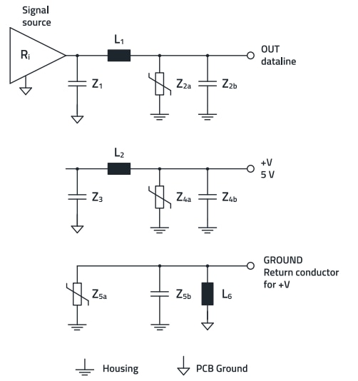
Figure 1: Unbalanced signal interface filter.
A digital (square wave) signal with amplitude of 5 VPP and frequency of 5 MHz on the data line is considered below. The standard value of 90 Ω is assumed for the impedance of long data signal lines. There is a voltage of 5 VDC at 2 A on the supply voltage line.
Since the requirements for the filter circuits for the data line and the supply voltage line differ, the filtering of the data line will be described first.
2.1 Filter circuit of the data line
To attenuate high-frequency interference on the data line, the two impedances Z1 and Z2b in Figure 2 form a low-pass π filter with the inductor. Protection against transient overvoltage is ensured by a transient protection device Z2a.
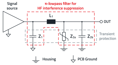
Figure 2: Filter on the data line of an unbalanced signal interface.
The component selection is explained below using the example of the signal driver described above.
Step 1: Determination of L1
First, L1 is dimensioned and selected, where an SMT ferrite or an RF–ferrite can be used. Further information on the use of inductors or SMT ferrites is given in ANP025 and in ANP129.
The ohmic, or resistive, component of the impedance of the SMT ferrite should be as low as possible up to the fifth harmonic of the signal frequency, and the impedance at this frequency should be less than one-tenth of the system impedance to avoid affecting the useful signal. In our example, the fifth harmonic is at 25 MHz, as the signal frequency is a 5 MHz square wave. Since the system impedance in the example is 90 Ω, the impedance at 25 MHz should be at most about one-tenth, i.e., no more than 9 Ω.
Figure 3 shows a typical impedance curve as seen in the data sheets. The proper inductors, in the example a SMT-ferrite can be selected with the help of REDEXPERT.
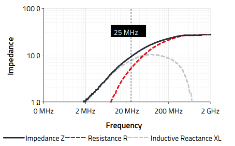
Figure 3: Impedance characteristics WE-CBF SMT ferrite 74279273.
From Figure 3, it can be concluded that WE-CBF 74279273 SMT ferrite can be used.
Step 2: Determination of Z1
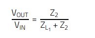
Z1 is a capacitor that can be optionally used to attenuate interference frequencies in the RF range above 500 MHz originating from the driver. Based on practical experience, a desired attenuation of 10 dB should be achieved at 500 MHz, resulting in a voltage ratio of VOUT/VIN = 0.316. The capacitor impedance Z1 (capacitive reactance) can be determined using the voltage divider in Figure 4.
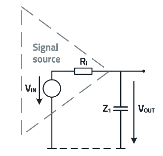
Figure 4: Voltage divider for calculating the capacitor Z1
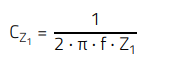
 (1)
(1)
Where:
- VOUT is the voltage across the capacitor Z1 (V).
- VIN is the total input voltage to the circuit (V).
- VOUT/VIN is the voltage ratio from the attenuation.
- Ri is the internal resistance of the signal source or system impedance (Ω).
- Z1 is the capacitor impedance (capacitive reactance) (Ω).
Given Ri = 90 Ω, the calculated Z1 from (1) is approximately 42 Ω. Next, the capacitance value (CZ1) required for attenuation at f = 500 MHz can be calculated as follows:
 (2)
(2)
Substituting the known values in (2),
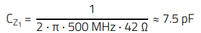
Based on these calculations, the WCAP-CSGP 885012005040 MLCC capacitor with a value of 10 pF and a voltage withstand rating of 25 V is suitable. This capacitor is an NP0 ceramic type, offering more stable voltage and temperature behavior compared to X7R ceramics. When considering critical factors such as signal integrity due to the cutoff frequency of the filter and the capacitive load, it's important to account for parasitic capacitances of the conductor tracks and, if necessary, interface connectors.
Step 3: Determination of Z2
Z2 consists of a component for transient protection (Z2a) and a capacitor (Z2b), whereby the parasitic capacitance of the transient protection device such as a TVS diode or a SMT varistor additionally contributes to the capacitance of the π filter. If the capacitance of the transient protection is high enough to achieve the required attenuation of 3 dB at 25 MHz (VOUT/VIN = 0.707), the capacitor may not be needed.
The advantages of a varistor compared to a TVS diode are the higher parasitic capacitance, a shorter response time and the ability to absorb more energy with the same component size.
The procedure for selecting Z2 is the same, using the following voltage divider with VOUT/VIN and ZL1:
 (3)
(3)
Where:
- VOUT/VIN is the voltage ratio from the attenuation.
- ZL1 is the impedance of the ferrite at 25 MHz with ZL1 = 10 Ω.
- Z2 represents the total impedance of Z2a and Z2b (Ω).
From this, we calculate the impedance and capacitance required for the Z2:
- Impedance: Z2 ≈ 25 Ω
- Therefore, capacitance needed: CZ2 ≈ 250 pF
The operating voltage of the varistor must be greater than the maximum operating voltage of the system, which here is 5 V.
Considering a safety buffer of 15%, the maximum operating voltage of the varistor is VDC > 5.75 V.
Based on this value and the available space in the application, an SMT multilayer varistor is selected, which serves as the basis for the decision. In this case, the WE-VS 82536040 (Table 1) varistor is selected, whose operating voltage (VDC) is 5.5 V and is therefore slightly below the required operating voltage. Once the varistor has been selected, the following calculations determine whether the correct selection has been made or not.
According to the IEC/EN 61000-4-5 standard, the test pulse for surge between line and ground is VSURGE = 0.5 kV and the source impedance is 42 Ω.
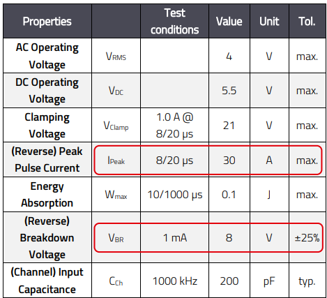
Table 1: Electrical properties of WE-VS 82536040.
To simplify our calculation, we specify the clamping voltage during the current surge as twice the breakdown voltage VBR. This value (2 x 8 = 16 V vs. clamping at 21 V) is slightly lower than the actual clamping voltage of the varistor at the surge current.
Approximation: VCLAMP ~ 2 VBR.
The varistor voltage (VVAR or VBR) can be found in the varistor data sheet (see Table 1).
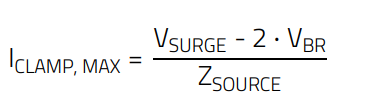
The peak varistor current can be calculated as follows:
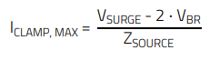 (4)
(4)
Where:
- ICLAMP, MAX is the peak current of the varistor (A).
- VSURGE is the test pulse voltage for surge (V).
- VBR is the varistor voltage or breakdown voltage at 1 mA (V).
- ZSOURCE is the source impedance as per IEC/EN 61000-4-5 (Ω).
Substituting the known values in (4),
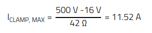
Considering the varistor tolerance of 25%, the maximum clamping current is 11.62 A and is therefore below the maximum peak current of the varistor (30 A).
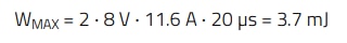
Energy consumption and power loss calculation:
To simplify our calculation, we assume that the pulse is a square signal with a pulse duration of 20 µs and the maximum clamping current of 11.6 A. The approximate energy can be calculated with twice the breakdown voltage and ICLAMP, MAX:
 (5)
(5)
Where:
- ICLAMP, MAX is the maximum clamping current.
- VBR is the varistor voltage or breakdown voltage at 1 mA (V).
- WMAX is the energy consumption of the varistor (J).
Substituting the known values in (5),
For the example above, the SMT Varistor WE-VS 82536040 with a capacitance of 200 pF for Z2a can be used.
To achieve the necessary capacitance, an additional capacitor with 47 pF in size 0805 is also used for Z2b in this case. The selected capacitor is the WCAP-CSGP 885012007080.
2.2 Filter circuit of the supply voltage line
In this section, the filter for the supply voltage cable entering the device is developed as shown in Figure 5.
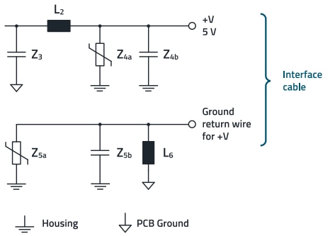
Figure 5: Power supply line filter of an unbalanced signal interface.
Generally, transients are filtered at interfaces against the housing - shown with the “housing” symbol. To enable a connection between the negative wire (GND of the USB cable line) to the functional ground (GND of the circuit board) and still attenuate interference coming from the cable, an SMT ferrite is used between the housing ground and GND. The capacitor Z5b and the parasitic capacitance of Z5a drain RF emissions with respect to transient voltages coming from the cable to the housing ground.
Step 1: Determination of Z3
A decoupling capacitor with 100 nF is used as standard here. A X7R ceramic capacitor with sufficient high rated voltage should be used here, so as not to run into the voltage bias effect and to lose capacitance.
Step 2: Determination of Z4 and Z5
Z4a is a SMT varistor with CCh = 200 pF.
To achieve the necessary capacitance for the filter, an additional capacitor of 100 nF is usually used as standard for Z4b, which should be the same capacitor as Z3.and Z5b. Varistors Z5a and Z4a should be the same component.
Step 3: Determination of L2 and L6
L2 and L6 are SMT ferrites, where the rated current should be considered first. This must be greater than 2 times the output current. In this example corresponds to 2 · 2 A = 4 A.
Minimum rated current of SMT ferrite: Ir = 4 A
Supply voltage lines have no cutoff frequency and a very low source impedance of approx. ZOUT ≈ 2 ··· 9 Ω. As the noise source is the +V line, all other signal sources on the electronic board will create RF noise to the +V network which must be considered. This means that the impedance ZL2 or ZL6 should be as high as possible across the entire signal frequency range (typically 30 MHz to 1 GHz) to achieve sufficiently strong attenuation. The selection of the proper SMT ferrite should be done by REDEXPERT to get the right impedance over the relevant frequency range. The ferrite selected here is the WE-CBF SMT EMI Suppression Ferrite Bead 74279252. The impedance chart is shown in Figure 6 and the electrical properties from the data sheet are shown in Table 2.
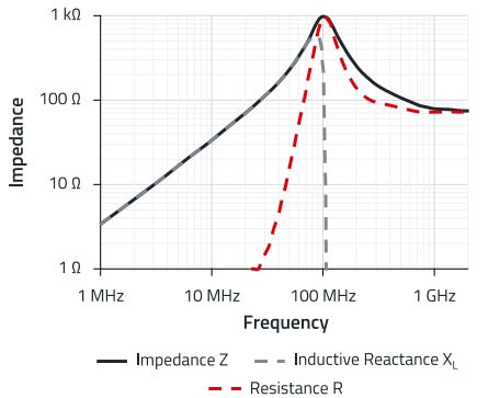
Figure 6: Impedance characteristics of SMT ferrite CBF 74279252
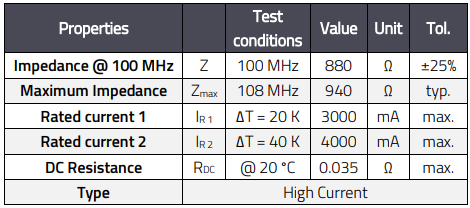
Table 2: Electrical properties of the SMT ferrite CBF 74279252.
Remark to Electrical Grounding
Unlike earthing for electrical safety in the sense of the Low Voltage Directive, the ground is a reference point for high-frequency signals in terms of EMC. Accordingly, the reference ground must have a low impedance and be free of high frequency "offset signals" and provide a reference point for filters and TVS components. The best reference is a very conductive metal housing.
3. EMI FILTER OF A SYMMETRICAL SIGNAL INTERFACE WITH TRANSIENT PROTECTION
Balanced signal interfaces use differential signal pairs to transmit information and to attenuate common-mode interference. However, these interfaces are still susceptible to radiated electromagnetic interference and the coupling of transient voltages and currents.
To reduce unwanted interference that can affect signal quality and system operation, additional filtering of the interface is essential. A good EMI filter reduces electromagnetic emissions from the signal source to the cable and vice versa, limits transient external interference to a tolerable level and has only a negligible effect on the signal integrity of the interface.
Figure 7 depicts a possible filter circuit for a balanced signal interface. The circuit utilizes a soft low-pass filter to pass the signal in differential mode while attenuating common-mode components.
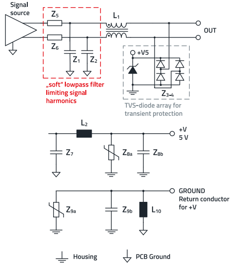
Figure 7: Balanced signal interface filter.
The symmetric low-pass filter allows differential-mode signals, which carry the essential information, to pass through unimpeded. Conversely, common-mode signals, which are noise components of the signal, are attenuated or damped by the filter.
TVS-diode array provides transient voltage protection. These spikes are sudden, unwanted bursts of high voltage that can damage electronic components. When a transient overvoltage occurs, the TVS diodes limit the voltage and divert the transient impulse current from the circuit to ground (housing).
The next section provides a practical example of component selection for a USB 2.0 interface. The USB 2.0 interface is a widely used for data and power transfer between electronic devices. It provides a signal bandwidth of approximately 240 MHz (480 Mbps) and an impedance of 90 Ω. A typical power supply for USB 2.0 is +5 V with a maximum current of 1 A.
3.1 Component Selection for USB 2.0 Interface
Step 1: Determination of L1
L1 is an inductor with high impedance for common-mode noise that allows differential signals to pass with minimal attenuation in the relevant signal frequency range. L1 selection is crucial in terms of differential and common-mode impedance needs. To ensure proper signal transmission, choke L1 should be selected according to the interface type and datasheet information, taking the following parameters into account:
System/Interface Impedance (ZSYSTEM):
ZSYSTEM can influence EMI filter design. Obtain the system or interface impedance from the data sheet or specifications.
Differential-mode Impedance (ZDM):
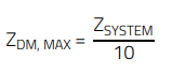
The choke impedance in the differential mode should be lower than 1/10 of the system impedance (ZSYSTEM) at the highest frequency within the signal bandwidth. This ensures minimal attenuation of the desired signals. Calculate the maximum allowed impedance for L1 in the differential mode:
 (6)
(6)
Common-mode Impedance (ZCM):
ZCM should be as high as possible, especially at frequencies corresponding to expected interference. At center frequency ZCM should be higher than ZSYSTEM. Select a choke (L1) with a high ZCM, especially at frequencies of expected interference. Pay attention to the frequency response, current handling capability, and other relevant parameters of the choke.
A suitable choke with a differential-mode impedance less than ZDM, MAX and a high common-mode impedance ZCM for our application is the WE-CNSW HF SMT common-mode line filter 744233900.
Step 2: Determination of Z1, Z2, Z5 and Z6
Capacitors (Z1, Z2) and matching resistors (Z5, Z6) form a "soft" low pass filter to limit signal harmonics or HF noise produced by the controller, resp. signal transceiver. The values of the resistors depend on the signal controller and its imbalance/mismatch and must be selected according to the measurement results. The values of Z5, Z6 are typically between 3 and 10 Ω. The capacitor values must be selected accordingly, the values vary in the range of 2.2 to 10 pF. Typical value for USB 2.0: 4.7 pF, e.g., WCAP-CSGP Ceramic Capacitor 885012005038.
The resistors Z5, Z6 (e.g., 3.3 Ω) are typically used for reflection damping and filtering in conjunction with the capacitors (Z1, Z2) to improve signal integrity and reduce interference. RF suitable types with a small body size should be used here.
Step 3: Determination of Z3, Z4, L2, Z7 and Z8
TVS diodes (Z3, Z4) and components like L2, Z7, and Z8 provide transient protection against voltage spikes and surges. To properly handle transient currents, consider the minimum rated current (Ir) of components such as L2 and the SMT ferrite (Z9a). L2, Z7, and Z8 are used for low cut-off frequency filtering, typically less than 1 MHz.
SMT Ferrite Bead (L2): Used for low cut-off frequency. Ensure the choke has an appropriate minimum rated current Ir. To achieve broadband noise reduction, the SMD ferrite WE-CBF SMT EMI Suppression Ferrite Bead 742792032 (see Table 3).
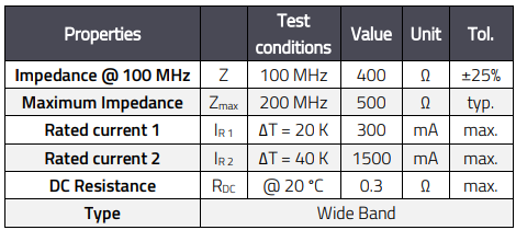
Table 3: Electrical properties of the SMT ferrite CBF 742792032.
Capacitors and Varistors (Z7, Z8): Z7 is a capacitor for low cut-off frequency filtering and Z8 is a SMT varistor for transient protection. An example of a suitable capacitor for this application is WCAP-CSGP Ceramic Capacitor 885012206120 and for a varistor, WE-VS SMT Varistor 82536040.
TVS Diodes Array (Z3, Z4): TVS diode arrays (Transient Voltage Suppression Arrays), such as the WE-TVS diode 8240136 from the "High Speed" series, are used to protect signal lines against transient voltages. It is important to note that these components also exhibit parasitic capacitance, which must not be too high relative to the data transfer rate or signal bandwidth. Information regarding suitable applications can be found in the datasheets.
Step 4: Determination of Z9a and Z9b
For high-frequency decoupling between housing and cable ground (GND), SMT ferrites (L10) and SMT varistors ( Z9a and Z9b), e.g., WE-CBF SMT EMI Suppression Ferrite Bead and WE-VS SMT varistor are used in combination with capacitors. This filter section helps reduce common-mode interference and improves system stability. Ensure that the current-carrying components are compatible with the required minimum rated current (Ir).
4. POWER LINE FILTER WITH TRANSIENT PROTECTION
A power line filter of protection class I with a protective conductor is considered below.
The circuit diagram in Figure 8 contains all components that are necessary for the filter circuit. The choke L1 decouples the load, i.e. the power supply, from the mains with its common-mode impedance. This means that the choke is RF-technically with Z1/Z6 and Z2/Z7 when the reference ground (PCB ground to housing) carries interference potential. However, Z6 and Z7 are capacitors with a low capacitance (typically 200 - 470 pF) that are inserted to dampen highfrequency harmonics of the switching power supply. The two capacitors should be placed on the circuit board of the power supply if the proportion of switching harmonics on the power supply side is high, or if the reference ground (case ground) does not form a high-frequency stable reference point.
The chokes Z4 and Z5 are already partially covered by the leakage inductance of the common mode choke L1; Z4 and Z5 can also be provided for additional attenuation in the frequency range above 10 MHz.
A mains filter for an interface with a 50 Hz mains frequency and a voltage of 230 VAC serves as a calculation example.
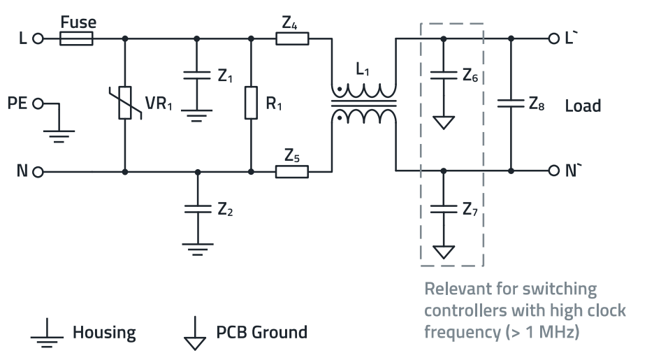
Figure 8: Circuit diagram of the line filter with transient protection.
The maximum permissible leakage current on PE is 3.5 mA according to DIN VDE 0701-0702 for electrical devices with rated voltages up to 1000 VAC/1500 VDC. For safety reasons, a maximum leakage current of ILEAK = 2.6 mA is assumed in the example, from which the maximum capacitance of the Y-capacitors (CY, MAX) with the mains filter frequency f = 50 Hz and the worst-case voltage of VMAINS = 257 V is calculated as follows
 (7)
(7)
Where:
- CY, MAX is the maximum capacitance of the Y-capacitor (F).
- ILEAK is the maximum leakage current (A).
- f is the mains frequency (Hz).
- VMAINS is the possible maximum value of the mains voltage.
Substituting the known values in (7),
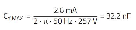
Thus, the maximum possible capacitance value of the Y-capacitor is therefore approximately 33 nF.
Step 1: Determination of L1
When designing the common-mode choke L1, the current carrying capacity (rated current Ir) depends on the load, the maximum ambient temperature and the maximum permissible leakage current must be considered.
The inductance of the common mode choke is defined depending on the current waveform of the AC-DC converter. For sinusoidal current consumption, a high inductance > 10 mH is used, while for non-sinusoidal current consumption, such as a switching regulator, low inductances in the range of 1 to 10 mH are used. In our example, a sinusoidal current is drawn and a common-mode choke with 10 mH is selected. The current-compensated mains choke WE CMB 744825410 can be used.
In the next step, the Y-capacitors Z1 and Z2, and the X-capacitor Z8 are selected.
Step 2: Determination of Z1, Z2 and Z8
Practical experience for the required minimum attenuation at 150 kHz is 20 dB in differential mode and 40 dB in commonmode. Common values for the filter corner frequencies are 15 kHz in differential mode and 10 kHz in common-mode. The corner frequency represents the frequency at which the attenuation of a filter is 3 dB. Given the required comer frequencies and required attenuation, the capacitances can be calculated:
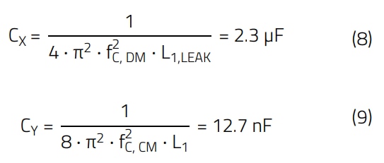
Where:
- fC, DM is the corner frequency of the differential-mode filter (Hz).
- fC, CM is the corner frequency of the common-mode filter (Hz).
- L1 is the inductance of the common-mode choke (H).
- L1,LEAK is the leakage inductance (H), which derived from L1/200 (empirical value).
Based on these values, for this example a capacitance of 2.2 µF is chosen for CX and a capacitance of 3 × 4.7 nF = 14.1 nF for CY. For the Y-capacitors the MLCC Safety Capacitors are used (WCAP-CSSA Interference Suppression). This results for the attenuation are shown in Figure 9.
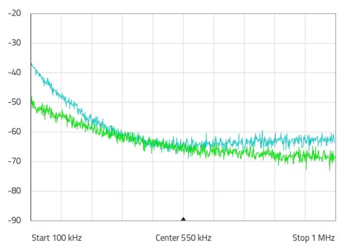
Figure 9: Differential-mode (green) and common-mode (blue) attenuation by Z1, Z2 and Z8.
The required attenuation of 20 dB at 150 kHz is exceeded by 32 dB in differential mode. The common-mode attenuation of 40 dB at 150 kHz can also be easily achieved with 43 dB.
For transient protection, a disk varistor is used in parallel to the X-capacitor, which is selected next.
Step 3: Determination of VR1
There are various approaches to the selection process, such as empirical testing of similar products, selection based on the specific electrical environmental conditions, or the surge test according to IEC/EN 61000-4-5 as a fundamental EMC test. The following section uses the IEC/EN 61000-4-5 standard as the basis.
When selecting the disk varistor, the maximum operating voltage (VDC/RMS) is determined. For safety reasons, this is calculated with a buffer of typically 15% above the supply voltage. With the mains voltage of 230 VAC, the maximum operating voltage is VRMS = 264.5 VAC.
As can be seen in Table 4, the size of the varistors depends on the peak current to be clamped. The higher the rated current, the larger the component.
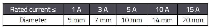
Table 4: Ratio of rated current to the diameter of varistors.
The disk varistor WE-VD 820443011E with a maximum operating voltage of VRMS = 300 V is used as the basis for the decision.
An excerpt from the data sheet can be seen in Table 5.
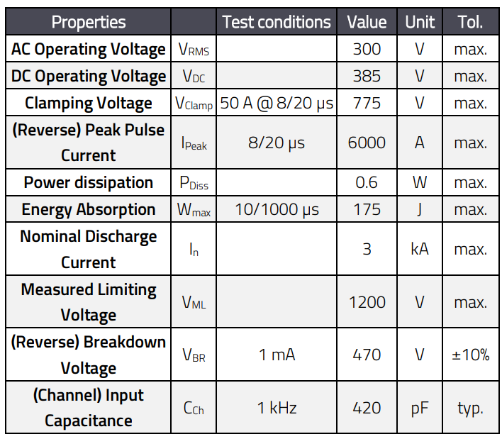
Table 5: Electrical properties of the disk varistor WE-VD 820443011E.
According to the IEC/EN 61000-4-5 standard, the voltage of the test pulse for surge between a conductor and a return conductor is VSURGE = 2 kV and the source impedance is 2 Ω for low voltage network connections between live conductor and neutral conductor.
The breakdown voltage (VVAR or VBR) can be found in the varistor datasheet (shown in Table 5). The peak current IPEAK can be calculated as follows:
 (10)
(10)
Where:
- ICLAMP, MAX is the peak current of the varistor (A).
- VSURGE is the test pulse for surge (V).
- VBR is the varistor voltage or breakdown voltage at 1 mA (V).
- ZSOURCE is the source impedance according to IEC/EN 61000-4-5 (Ω).
By substituting the known values into (10), the clamped peak current is obtained:
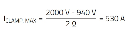
To simplify our calculation, we specify that the clamping voltage during the current surge is twice the breakdown voltage VBR. This value is slightly higher than the actual clamping voltage of the varistor at the surge current (refer to the diagram of the rated current vs. voltage in the datasheet).
Approximation: VCLAMP ~ 2 VBR.
Considering a tolerance of 10%, the maximum clamping current is 583 A and is therefore below the maximum peak current of the varistor (6000 A).
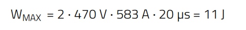
Energy consumption and power loss calculation:
To further simplify the calculation, it is assumed that the pulse is a rectangular signal that maintains its maximum current value over its 20 µs duration. Then the energy can be calculated with twice the breakdown voltage VBR and ICLAMP, MAX:
 (11)
(11)
Where:
- ICLAMP, MAX is the maximum clamping current.
- VBR is the varistor breakdown voltage at 1 mA (V).
- WMAX is the energy consumption of the varistor (J).
By substituting the known values into (11), the energy to be absorbed by the varistor is calculated:
The IEC/EN 61000-4-5 standard requires at least one surge impulse per minute during testing. The varistor must be able to dissipate this energy. The power requirement can be calculated from the energy and the time between two surge pulses as shown in (12).
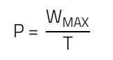 (12)
(12)
Where:
- P is the power dissipated by the varistor (W).
- WMAX is the energy consumption of the varistor (J).
- T is the time between two surge pulses (s).
Using the known values, the power is calculated according to the (12):
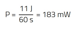
The varistor would therefore also be suitable for a surge interval of 20 seconds, whereby the power would then correspond to 549 mW and would therefore be below the maximum power loss of the selected varistor (600 mW).
5. CONCLUSION
This support note has explained the basis for transient suppression and basic EMI filtering for both data and power interfaces with worked examples of each that apply the principles discussed.
IMPORTANT NOTICE
The Application Note is based on our knowledge and experience of typical requirements concerning these areas. It serves as general guidance and should not be construed as a commitment for the suitability for customer applications by Würth Elektronik eiSos GmbH & Co. KG. The information in the Application Note is subject to change without notice. This document and parts thereof must not be reproduced or copied without written permission, and contents thereof must not be imparted to a third party nor be used for any unauthorized purpose. Würth Elektronik eiSos GmbH & Co. KG and its subsidiaries and affiliates (WE) are not liable for application assistance of any kind. Customers may use WE’s assistance and product recommendations for their applications and design. The responsibility for the applicability and use of WE Products in a particular customer design is always solely within the authority of the customer. Due to this fact it is up to the customer to evaluate and investigate, where appropriate, and decide whether the device with the specific product characteristics described in the product specification is valid and suitable for the respective customer application or not. The technical specifications are stated in the current data sheet of the products. Therefore, the customers shall use the data sheets and are cautioned to verify that data sheets are current. The current data sheets can be downloaded at www.we-online.com. Customers shall strictly observe any product-specific notes, cautions and warnings. WE reserves the right to make corrections, modifications, enhancements, improvements, and other changes to its products and services. WE DOES NOT WARRANT OR REPRESENT THAT ANY LICENSE, EITHER EXPRESS OR IMPLIED, IS GRANTED UNDER ANY PATENT RIGHT, COPYRIGHT, MASK WORK RIGHT, OR OTHER INTELLECTUAL PROPERTY RIGHT RELATING TO ANY COMBINATION, MACHINE, OR PROCESS IN WHICH WE PRODUCTS OR SERVICES ARE USED. INFORMATION PUBLISHED BY WE REGARDING THIRD-PARTY PRODUCTS OR SERVICES DOES NOT CONSTITUTE A LICENSE FROM WE TO USE SUCH PRODUCTS OR SERVICES OR A WARRANTY OR ENDORSEMENT THEREOF. WE products are not authorized for use in safety-critical applications, or where a failure of the product is reasonably expected to cause severe personal injury or death. Moreover, WE products are neither designed nor intended for use in areas such as military, aerospace, aviation, nuclear control, submarine, transportation (automotive control, train control, ship control), transportation signal, disaster prevention, medical, public information network etc. Customers shall inform WE about the intent of such usage before design-in stage. In certain customer applications requiring a very high level of safety and in which the malfunction or failure of an electronic component could endanger human life or health, customers must ensure that they have all necessary expertise in the safety and regulatory ramifications of their applications. Customers acknowledge and agree that they are solely responsible for all legal, regulatory and safety-related requirements concerning their products and any use of WE products in such safety-critical applications, notwithstanding any applicationsrelated information or support that may be provided by WE. CUSTOMERS SHALL INDEMNIFY WE AGAINST ANY DAMAGES ARISING OUT OF THE USE OF WE PRODUCTS IN SUCH SAFETYCRITICAL APPLICATION.
DIRECT LINK
SN024 | Transient suppression at different interfaces
USEFUL LINKS:
Application Notes : https://we-online.com/en/support/knowledge/application-notes
Services: https://we-online.com/en/products/components/service
Contact : https://we-online.com/en/support/contact
CONTACT INFORMATION
Würth Elektronik eiSos GmbH & Co. KG
Max-Eyth-Str. 1, 74638 Waldenburg, Germany
Tel.: +49 (0) 7942 / 945 – 0
Email: appnotes@we-online.de