element14 Community
element14 Community
    Register Log In
  • Site
  • Search
  • Log In Register
  • About Us
  • Community Hub
    Community Hub
    • What's New on element14
    • Feedback and Support
    • Benefits of Membership
    • Personal Blogs
    • Members Area
    • Achievement Levels
  • Learn
    Learn
    • Ask an Expert
    • eBooks
    • element14 presents
    • Learning Center
    • Tech Spotlight
    • STEM Academy
    • Webinars, Training and Events
    • Learning Groups
  • Technologies
    Technologies
    • 3D Printing
    • FPGA
    • Industrial Automation
    • Internet of Things
    • Power & Energy
    • Sensors
    • Technology Groups
  • Challenges & Projects
    Challenges & Projects
    • Design Challenges
    • element14 presents Projects
    • Project14
    • Arduino Projects
    • Raspberry Pi Projects
    • Project Groups
  • Products
    Products
    • Arduino
    • Avnet Boards Community
    • Dev Tools
    • Manufacturers
    • Multicomp Pro
    • Product Groups
    • Raspberry Pi
    • RoadTests & Reviews
  • Store
    Store
    • Visit Your Store
    • Choose another store...
      • Europe
      •  Austria (German)
      •  Belgium (Dutch, French)
      •  Bulgaria (Bulgarian)
      •  Czech Republic (Czech)
      •  Denmark (Danish)
      •  Estonia (Estonian)
      •  Finland (Finnish)
      •  France (French)
      •  Germany (German)
      •  Hungary (Hungarian)
      •  Ireland
      •  Israel
      •  Italy (Italian)
      •  Latvia (Latvian)
      •  
      •  Lithuania (Lithuanian)
      •  Netherlands (Dutch)
      •  Norway (Norwegian)
      •  Poland (Polish)
      •  Portugal (Portuguese)
      •  Romania (Romanian)
      •  Russia (Russian)
      •  Slovakia (Slovak)
      •  Slovenia (Slovenian)
      •  Spain (Spanish)
      •  Sweden (Swedish)
      •  Switzerland(German, French)
      •  Turkey (Turkish)
      •  United Kingdom
      • Asia Pacific
      •  Australia
      •  China
      •  Hong Kong
      •  India
      •  Korea (Korean)
      •  Malaysia
      •  New Zealand
      •  Philippines
      •  Singapore
      •  Taiwan
      •  Thailand (Thai)
      • Americas
      •  Brazil (Portuguese)
      •  Canada
      •  Mexico (Spanish)
      •  United States
      Can't find the country/region you're looking for? Visit our export site or find a local distributor.
  • Translate
  • Profile
  • Settings
PCB Design, Prototyping and Production
  • Products
  • More
PCB Design, Prototyping and Production
PCB Forum Good PCB design practices
  • Blog
  • Forum
  • Documents
  • Leaderboard
  • Files
  • Members
  • Mentions
  • Sub-Groups
  • Tags
  • More
  • Cancel
  • New
Join PCB Design, Prototyping and Production to participate - click to join for free!
Actions
  • Share
  • More
  • Cancel
Forum Thread Details
  • Replies 12 replies
  • Subscribers 122 subscribers
  • Views 2350 views
  • Users 0 members are here
  • kicad
  • pcb
  • pcb prototyping
  • pcb design
Related

Good PCB design practices

rsjawale24
rsjawale24 over 2 years ago

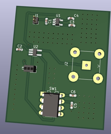
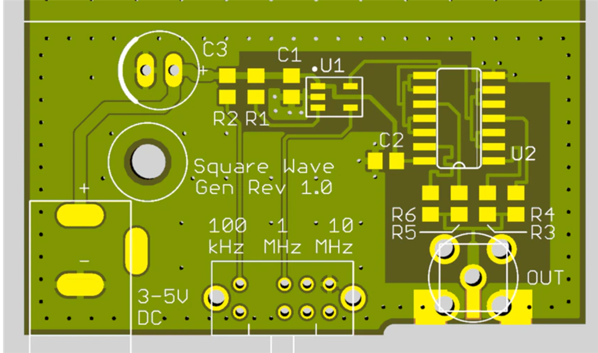
I'm working on an oscillator design using an off the shelf integrated circuit-based oscillator.

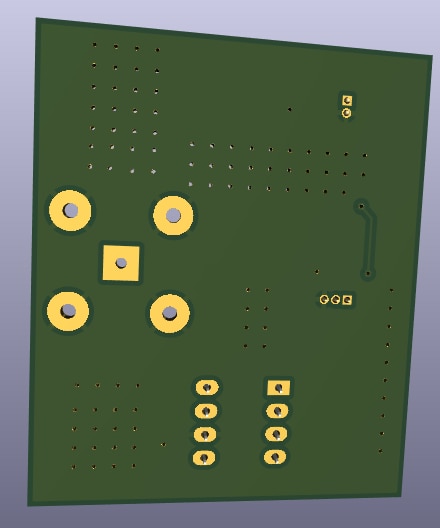
I have made two large gnd planes in the PCB, the top layer as well as the bottom layer. 

Is this a good practice esp. for making PCBs for applications like oscillators?

I have also added plenty of vias to connect the two layers. 

I just wanted suggestions (if any) before I send the PCB for fabrication. 

image

image

image

  • Sign in to reply
  • Cancel

Top Replies

  • wolfgangfriedrich
    wolfgangfriedrich over 2 years ago +2
    If you have top and bottom ground plane, it is essential to stitch them together with a lot of vias, so that is good. They should be positioned all the way up to the edge of the board. Also more vias at…
  • shabaz
    shabaz over 2 years ago in reply to shabaz +2
    EDIT: In fact, it looks like your project is doing a similar thing to mine, except for the sharper edges. Also, I'm using a multi-position slide-switch instead of a DIP switch, but it's all fairly similar…
  • wolfgangfriedrich
    wolfgangfriedrich over 2 years ago +2
    Some more ideas: 1) If you rotate C2 clockwise 90deg and move it closer to pins 1,2 of U2, the power trace could stay on the top layer. Also the power trace should be much thicker, 1mm (25 mil) as a…
  • wolfgangfriedrich
    wolfgangfriedrich over 2 years ago

    If you have top and bottom ground plane, it is essential to stitch them together with a lot of vias, so that is good. They should be positioned all the way up to the edge of the board. Also more vias at the top copper island between SW1 and U2.

    For your design, I assume the clock signal is from U2 pin5 the SMA connector. If you are using a 50 Ohm coax cable, the trace on the board should be 50 Ohm impedance as well. The ground plane on the bottom under the trance is absolutely required to make it a microstrip conductor for a controlled impedance signal. The ground plane on top is tricky in this case. In your layout, it is close enough to the signal trance to make it a co-planar waveguide. If you want to top ground plane have no impact on your impedance calculation it should be pulled bck from the trace >5x trace height over the bottom ground plane. 

    Saturn PCB calculator is a good tool for impadance calculation.

    • Cancel
    • Vote Up +2 Vote Down
    • Sign in to reply
    • Cancel
  • shabaz
    shabaz over 2 years ago

    For RF boards usually there would be vias right at the edge of the board as Wolfgang says, because the electric field can be terminated toward it (probably requires a textbook for a better explanation!). 

    The chip you're using (LTC1799) doesn't have particularly fast edges or clock rate, so I think you'll be OK, but worth adding in vias. 

    If it helps, there's a project using that chip here:  Building a Fast Edge Square Wave Generator 

    (the output was connected to buffers to sharpen up the edges for that project). As you can see, I did as Wolfgang refers to, with the top ground plane pulled back where it wasn't needed. The top plane is really useful for preventing the board from warping, but occasionally gets in the way. I have the tiniest 50 ohm trace because the rest of it wasn't 50 ohm characteristic impedance.

    image

    • Cancel
    • Vote Up 0 Vote Down
    • Sign in to reply
    • Cancel
  • shabaz
    shabaz over 2 years ago in reply to shabaz

    EDIT: In fact, it looks like your project is doing a similar thing to mine, except for the sharper edges. Also, I'm using a multi-position slide-switch instead of a DIP switch, but it's all fairly similar.

    If you prefer, you could just use the Gerber files at the blog post I mentioned, if this helps.

    • Cancel
    • Vote Up +2 Vote Down
    • Sign in to reply
    • Cancel
  • shabaz
    shabaz over 2 years ago in reply to shabaz

    (Or use it as a reference, because the output traces were quite reasonable with it).

    • Cancel
    • Vote Up 0 Vote Down
    • Sign in to reply
    • Cancel
  • wolfgangfriedrich
    wolfgangfriedrich over 2 years ago in reply to shabaz

    I agree with everything shabaz said. If fact, after seeing his board, you should check your through holes of the SMA footprint if they match the connector that you have selected. Their diameter looks very small for every SMA part I have ever seen. But then, maybe it is not SMA; could also be right angle BNC and my concern is not valid at all. 

    • Cancel
    • Vote Up +1 Vote Down
    • Sign in to reply
    • Cancel
  • wolfgangfriedrich
    wolfgangfriedrich over 2 years ago

    Some more ideas:

    1) If you rotate C2 clockwise 90deg and move it closer to pins 1,2 of U2, the power trace could stay on the top layer. Also the power trace should be much thicker, 1mm (25 mil) as a ballpark.

    2) Moving U2 closer to J2 and making the trace from pin5 to the connector center pin a straight line.

    3) SW: the traces connecting pins 1, 2, and 3 routed on the outside of the footprint would make the design more obvious when looking at the PCB and easier to cut if needed. Same for U1 pins1 and 3.

    4) If SW1 is a regular DIP8 footprint, the 2 jumpers J1 and J3 look like a pin distance of 1.27mm (50mil), which is half the size of a regular 0.1" jumper. I once had an eval board with those tiny bastards, they were terrible to handle (2nd picture on the linked post).

     Vishay microBUCK SiC461 Eval Board 

    • Cancel
    • Vote Up +2 Vote Down
    • Sign in to reply
    • Cancel
  • shabaz
    shabaz over 2 years ago in reply to wolfgangfriedrich

    1.27mm pin headers are the worst! : ) The board size looks spacious so normal 0.1" would fit anyway. 

    • Cancel
    • Vote Up +1 Vote Down
    • Sign in to reply
    • Cancel
  • rsjawale24
    rsjawale24 over 2 years ago in reply to wolfgangfriedrich

    Thanks, I'll add more vias new SW1 and U2.
    No, I'm not looking for 50ohms impedance match. I'm aware about the transmission line designs Slight smile

    This osc. LTC1799 goes max upto 33MHz. I'll be using it just as a signal generator and to experiment with my new USB oscilloscope.

    • Cancel
    • Vote Up 0 Vote Down
    • Sign in to reply
    • Cancel
  • rsjawale24
    rsjawale24 over 2 years ago in reply to shabaz

    Yes, the vias along the edge of the PCB act as a wall for the electic field and the field remains confined to the board. It is called as SIW (Substrate Integrated Waveguide). However, considering that this is pretty low freq. (LTC1799 can go upto 33MHz only) so I'm have skipped things like 50 ohms line, matching and edge vias but I think It's better to add those vias as it will improve the performance.

    I'm an RF engineer so I'm well aware about those rules Slight smile But those rules are more critical above few 100's of MHz and GHz range, so I decided to skip it.

    Another reason to not include the 50 ohm trace is my oscilloscope only has a High Z port. So designing a 50 ohms trace and using 50 ohms connector will anyway give a mismatch. Also, I tried assembling LTC1799 on a small perfboard and directly connected the probe at the output, it just worked fine.

    Anyway, thanks for the inputs. I'll do slight changes in the design.

    • Cancel
    • Vote Up 0 Vote Down
    • Sign in to reply
    • Cancel
  • rsjawale24
    rsjawale24 over 2 years ago in reply to wolfgangfriedrich

    Yes, I have used a BNC connector

    • Cancel
    • Vote Up 0 Vote Down
    • Sign in to reply
    • Cancel
>
element14 Community

element14 is the first online community specifically for engineers. Connect with your peers and get expert answers to your questions.

  • Members
  • Learn
  • Technologies
  • Challenges & Projects
  • Products
  • Store
  • About Us
  • Feedback & Support
  • FAQs
  • Terms of Use
  • Privacy Policy
  • Legal and Copyright Notices
  • Sitemap
  • Cookies

An Avnet Company © 2025 Premier Farnell Limited. All Rights Reserved.

Premier Farnell Ltd, registered in England and Wales (no 00876412), registered office: Farnell House, Forge Lane, Leeds LS12 2NE.

ICP 备案号 10220084.

Follow element14

  • X
  • Facebook
  • linkedin
  • YouTube