element14 Community
element14 Community
    Register Log In
  • Site
  • Search
  • Log In Register
  • Community Hub
    Community Hub
    • What's New on element14
    • Feedback and Support
    • Benefits of Membership
    • Personal Blogs
    • Members Area
    • Achievement Levels
  • Learn
    Learn
    • Ask an Expert
    • eBooks
    • element14 presents
    • Learning Center
    • Tech Spotlight
    • STEM Academy
    • Webinars, Training and Events
    • Learning Groups
  • Technologies
    Technologies
    • 3D Printing
    • FPGA
    • Industrial Automation
    • Internet of Things
    • Power & Energy
    • Sensors
    • Technology Groups
  • Challenges & Projects
    Challenges & Projects
    • Design Challenges
    • element14 presents Projects
    • Project14
    • Arduino Projects
    • Raspberry Pi Projects
    • Project Groups
  • Products
    Products
    • Arduino
    • Avnet & Tria Boards Community
    • Dev Tools
    • Manufacturers
    • Multicomp Pro
    • Product Groups
    • Raspberry Pi
    • RoadTests & Reviews
  • About Us
    About the element14 Community
  • Store
    Store
    • Visit Your Store
    • Choose another store...
      • Europe
      •  Austria (German)
      •  Belgium (Dutch, French)
      •  Bulgaria (Bulgarian)
      •  Czech Republic (Czech)
      •  Denmark (Danish)
      •  Estonia (Estonian)
      •  Finland (Finnish)
      •  France (French)
      •  Germany (German)
      •  Hungary (Hungarian)
      •  Ireland
      •  Israel
      •  Italy (Italian)
      •  Latvia (Latvian)
      •  
      •  Lithuania (Lithuanian)
      •  Netherlands (Dutch)
      •  Norway (Norwegian)
      •  Poland (Polish)
      •  Portugal (Portuguese)
      •  Romania (Romanian)
      •  Russia (Russian)
      •  Slovakia (Slovak)
      •  Slovenia (Slovenian)
      •  Spain (Spanish)
      •  Sweden (Swedish)
      •  Switzerland(German, French)
      •  Turkey (Turkish)
      •  United Kingdom
      • Asia Pacific
      •  Australia
      •  China
      •  Hong Kong
      •  India
      •  Japan
      •  Korea (Korean)
      •  Malaysia
      •  New Zealand
      •  Philippines
      •  Singapore
      •  Taiwan
      •  Thailand (Thai)
      •  Vietnam
      • Americas
      •  Brazil (Portuguese)
      •  Canada
      •  Mexico (Spanish)
      •  United States
      Can't find the country/region you're looking for? Visit our export site or find a local distributor.
  • Translate
  • Profile
  • Settings
PCB Design, Prototyping and Production
  • Products
  • More
PCB Design, Prototyping and Production
PCB Forum Look for KiCAD symbol and footprint resource for an LoRa module
  • Blog
  • Forum
  • Documents
  • Leaderboard
  • Files
  • Members
  • Mentions
  • Sub-Groups
  • Tags
  • More
  • Cancel
  • New
Join PCB Design, Prototyping and Production to participate - click to join for free!
Actions
  • Share
  • More
  • Cancel
Forum Thread Details
  • Replies 10 replies
  • Subscribers 160 subscribers
  • Views 2140 views
  • Users 0 members are here
  • kicad
  • footprint
  • symbols
Related

Look for KiCAD symbol and footprint resource for an LoRa module

colporteur
colporteur over 1 year ago

image

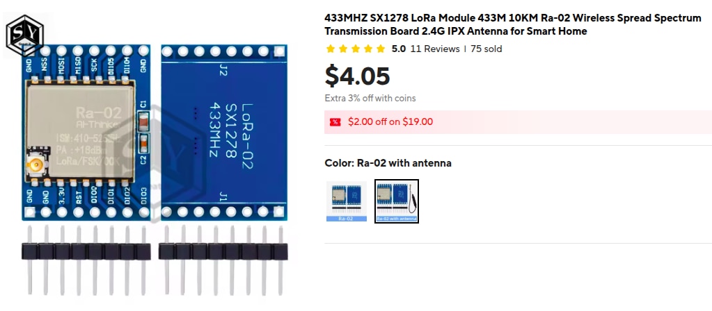
A friend has asked me to design a PCB that uses this module.

I used the capitalized word that begins with F, to voice my frustration on having to create the symbol and footprint for the beast. I need to blow off my notes from two versions of KiCAD ago. Then I thought, maybe someone in the E14 community had done it already and is willing to share.

Anyone have KiCAD 8 resources for this module?

  • Sign in to reply
  • Cancel

Top Replies

  • Gough Lui
    Gough Lui over 1 year ago +3
    Are you using the AI-Thinker Ra-02 module itself or the WHOLE unit including the blue break-out PCB? If using the break-out PCB, that's standard 2.54mm SIL header so you could merely get away with using…
  • beacon_dave
    beacon_dave over 1 year ago +3
    If all else fails, then Shabaz created a blog and video on how to create your own component symbols: /products/pcbprototyping/b/pcb-blogs/posts/kicad-quick-tutorial-creating-component-symbols and Jan…
  • shabaz
    shabaz over 1 year ago in reply to beacon_dave +2
    Thanks Dave, Also, there's a footprint tutorial too: KiCad Quick Tutorial: Creating Component Footprints with the help of a Wizard An easy way to dip toes in the water would be to copy a closely…
  • Gough Lui
    Gough Lui over 1 year ago

    Are you using the AI-Thinker Ra-02 module itself or the WHOLE unit including the blue break-out PCB? If using the break-out PCB, that's standard 2.54mm SIL header so you could merely get away with using two header-pin rows, making sure the rows are properly spaced in the PCB layout.

    Otherwise, if you're only using the Ra-02 module, the symbol/footprint/model can be downloaded from here - www.snapeda.com/.../

    • Cancel
    • Vote Up +3 Vote Down
    • Sign in to reply
    • Cancel
  • beacon_dave
    beacon_dave over 1 year ago

    If all else fails, then Shabaz created a blog and video on how to create your own component symbols:

    /products/pcbprototyping/b/pcb-blogs/posts/kicad-quick-tutorial-creating-component-symbols

    and Jan shows off alternate pin function definitions:

    /products/pcbprototyping/f/forum/54473/kicad-8-alternative-pin-functions

    • Cancel
    • Vote Up +3 Vote Down
    • Sign in to reply
    • Cancel
  • Jan Cumps
    Jan Cumps over 1 year ago

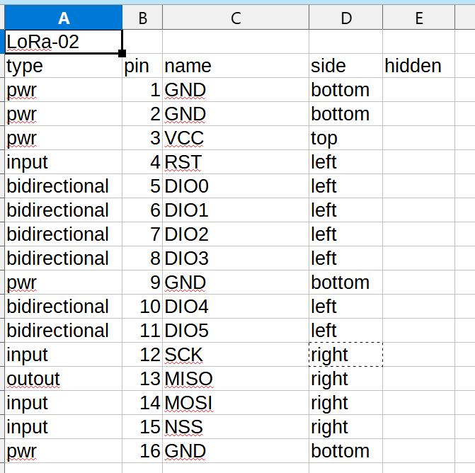
    I made a schema symbol with KiPart  KiCAD lovers, check out KiPart 

    image

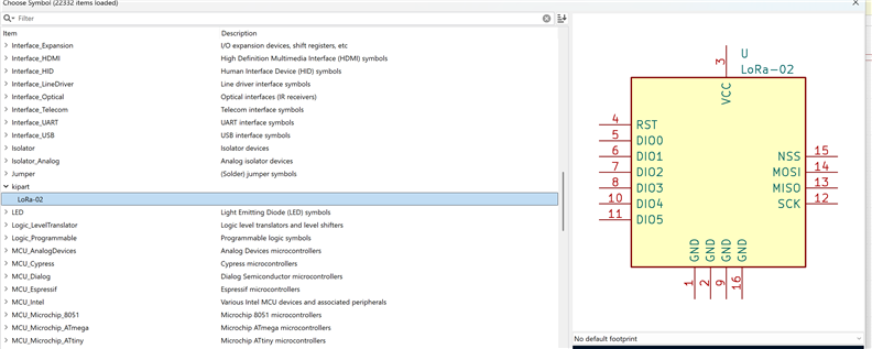
    Imported the resulting library in KiCad, and migrated it (because KiPart makes legacy .lib libraries)

    image

    LoRa-02.zip

    • Cancel
    • Vote Up +1 Vote Down
    • Sign in to reply
    • Cancel
  • colporteur
    colporteur over 1 year ago in reply to Jan Cumps

    I vaguely recall this but never had a reason to invest. Looks like I do now. Thanks J.

    • Cancel
    • Vote Up 0 Vote Down
    • Sign in to reply
    • Cancel
  • Jan Cumps
    Jan Cumps over 1 year ago in reply to colporteur

    I attached the library to the comment above

    • Cancel
    • Vote Up +1 Vote Down
    • Sign in to reply
    • Cancel
  • shabaz
    shabaz over 1 year ago in reply to beacon_dave

    Thanks Dave,

    Also, there's a footprint tutorial too:

     KiCad Quick Tutorial: Creating Component Footprints with the help of a Wizard 

    An easy way to dip toes in the water would be to copy a closely similar symbol or footprint (e.g. a 16-pin DIP IC isn't that dissimilar from what's required, just that the rows need to be farther apart) using Save As, and then editing that. Or use the Wizard, since it's very well geared up for pins/pads in dual rows, since that's a popular form-factor.

    • Cancel
    • Vote Up +2 Vote Down
    • Sign in to reply
    • Cancel
  • colporteur
    colporteur over 1 year ago in reply to shabaz

    I'm in a quandary. Member solutions gave me an easy way out. Thanks folks! I want to do the work and put in the effort. I get so much from learning. Time constraints are making that hard.

    • Cancel
    • Vote Up 0 Vote Down
    • Sign in to reply
    • Cancel
  • colporteur
    colporteur over 1 year ago in reply to Jan Cumps

    Saw what you posted and wanted to immediately go down stairs and try it. Clearer head prevailed and I drank my morning coffee in the sun instead.

    • Cancel
    • Vote Up +1 Vote Down
    • Sign in to reply
    • Cancel
  • mp2100
    mp2100 over 1 year ago

    Mostly off-topic, but, you are in the US, correct?  The photo shows a 433 Mhz LoRa module.  You have use a 915 MHz board in the US.

    Allen

    • Cancel
    • Vote Up 0 Vote Down
    • Sign in to reply
    • Cancel
  • colporteur
    colporteur over 1 year ago in reply to mp2100

    No. North of the border. The symbol and foot print seemed to match.

    • Cancel
    • Vote Up 0 Vote Down
    • Sign in to reply
    • Cancel
element14 Community

element14 is the first online community specifically for engineers. Connect with your peers and get expert answers to your questions.

  • Members
  • Learn
  • Technologies
  • Challenges & Projects
  • Products
  • Store
  • About Us
  • Feedback & Support
  • FAQs
  • Terms of Use
  • Privacy Policy
  • Legal and Copyright Notices
  • Sitemap
  • Cookies

An Avnet Company © 2026 Premier Farnell Limited. All Rights Reserved.

Premier Farnell Ltd, registered in England and Wales (no 00876412), registered office: Farnell House, Forge Lane, Leeds LS12 2NE.

Follow element14

  • X
  • Facebook
  • linkedin
  • YouTube