element14 Community
element14 Community
    Register Log In
  • Site
  • Search
  • Log In Register
  • Community Hub
    Community Hub
    • What's New on element14
    • Feedback and Support
    • Benefits of Membership
    • Personal Blogs
    • Members Area
    • Achievement Levels
  • Learn
    Learn
    • Ask an Expert
    • eBooks
    • element14 presents
    • Learning Center
    • Tech Spotlight
    • STEM Academy
    • Webinars, Training and Events
    • Learning Groups
  • Technologies
    Technologies
    • 3D Printing
    • FPGA
    • Industrial Automation
    • Internet of Things
    • Power & Energy
    • Sensors
    • Technology Groups
  • Challenges & Projects
    Challenges & Projects
    • Design Challenges
    • element14 presents Projects
    • Project14
    • Arduino Projects
    • Raspberry Pi Projects
    • Project Groups
  • Products
    Products
    • Arduino
    • Avnet & Tria Boards Community
    • Dev Tools
    • Manufacturers
    • Multicomp Pro
    • Product Groups
    • Raspberry Pi
    • RoadTests & Reviews
  • About Us
  • Store
    Store
    • Visit Your Store
    • Choose another store...
      • Europe
      •  Austria (German)
      •  Belgium (Dutch, French)
      •  Bulgaria (Bulgarian)
      •  Czech Republic (Czech)
      •  Denmark (Danish)
      •  Estonia (Estonian)
      •  Finland (Finnish)
      •  France (French)
      •  Germany (German)
      •  Hungary (Hungarian)
      •  Ireland
      •  Israel
      •  Italy (Italian)
      •  Latvia (Latvian)
      •  
      •  Lithuania (Lithuanian)
      •  Netherlands (Dutch)
      •  Norway (Norwegian)
      •  Poland (Polish)
      •  Portugal (Portuguese)
      •  Romania (Romanian)
      •  Russia (Russian)
      •  Slovakia (Slovak)
      •  Slovenia (Slovenian)
      •  Spain (Spanish)
      •  Sweden (Swedish)
      •  Switzerland(German, French)
      •  Turkey (Turkish)
      •  United Kingdom
      • Asia Pacific
      •  Australia
      •  China
      •  Hong Kong
      •  India
      • Japan
      •  Korea (Korean)
      •  Malaysia
      •  New Zealand
      •  Philippines
      •  Singapore
      •  Taiwan
      •  Thailand (Thai)
      • Vietnam
      • Americas
      •  Brazil (Portuguese)
      •  Canada
      •  Mexico (Spanish)
      •  United States
      Can't find the country/region you're looking for? Visit our export site or find a local distributor.
  • Translate
  • Profile
  • Settings
Raspberry Pi
  • Products
  • More
Raspberry Pi
Raspberry Pi Forum I've killed my gertboard ! ( and havent even finished it )
  • Blog
  • Forum
  • Documents
  • Quiz
  • Events
  • Polls
  • Files
  • Members
  • Mentions
  • Sub-Groups
  • Tags
  • More
  • Cancel
  • New
Join Raspberry Pi to participate - click to join for free!
Featured Articles
Announcing Pi
Technical Specifications
Raspberry Pi FAQs
Win a Pi
Raspberry Pi Wishlist
Actions
  • Share
  • More
  • Cancel
Forum Thread Details
  • Replies 14 replies
  • Subscribers 681 subscribers
  • Views 1252 views
  • Users 0 members are here
  • raspberry_pi
  • gertboard_kit
Related

I've killed my gertboard ! ( and havent even finished it )

Former Member
Former Member over 13 years ago

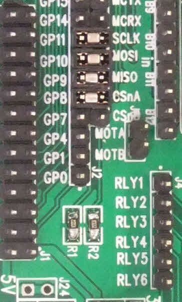
Well this is amusing.. Whilst attempting to solder one of the grains of sand in the kit,  I've managed to burn a couple of surfacemount pads on the board  image.  It's on one of the resistors,  I think I had the iron way to hot.


I was wondering ( hoping )  if anyone could advise on a way to fix it..


Thanks in advance.


Ash.

  • Sign in to reply
  • Cancel
Parents
  • Former Member
    Former Member over 13 years ago

    image


    It's the R1 pads, both of them, rather than the view above,, I have two brown marks where the pads used to be.. 


    I have invested in a decent iron since..lol


    I'll try and pick up some of the AWG30 and have a go at a repair.


    https://community.element14.com/resized-image/__size/1200x900/__key/communityserver-discussions-components-files/91/3821.contentimage_5F00_175229.html


    Ash.

    • Cancel
    • Vote Up 0 Vote Down
    • Sign in to reply
    • Cancel
  • johnbeetem
    johnbeetem over 13 years ago in reply to Former Member

    According to the Gertboard schematic from rev 1.0 of the Gertboard User Manual, R1 and R2 are both pull-ups to +3.3V.  So I think you can just connect the labeled ends of R1 and R2 using a short non-insulated jumper wire.  For the other end of R1, you could scrape the solder resist off the diagonal trace and solder a short bare wire to the exposed trace.  You'll need a sharp X-acto knife or equivalent and stop scraping as soon as you see metal.  Then pre-tin the trace by heating it up with your soldering iron while melting solder onto the trace.  This makes it much easier to solder the actual wire to R1.  Be careful not to short to the copper fill beside the trace.


    You could also make the repair on the back side of the board, soldering one end of R1 to the through-hole pin it's supposed to pull up (J11 pin 4) and solder an insulated wire to +3.3V (J7 pin 2) from the other end of R1.

    • Cancel
    • Vote Up +1 Vote Down
    • Sign in to reply
    • Cancel
Reply
  • johnbeetem
    johnbeetem over 13 years ago in reply to Former Member

    According to the Gertboard schematic from rev 1.0 of the Gertboard User Manual, R1 and R2 are both pull-ups to +3.3V.  So I think you can just connect the labeled ends of R1 and R2 using a short non-insulated jumper wire.  For the other end of R1, you could scrape the solder resist off the diagonal trace and solder a short bare wire to the exposed trace.  You'll need a sharp X-acto knife or equivalent and stop scraping as soon as you see metal.  Then pre-tin the trace by heating it up with your soldering iron while melting solder onto the trace.  This makes it much easier to solder the actual wire to R1.  Be careful not to short to the copper fill beside the trace.


    You could also make the repair on the back side of the board, soldering one end of R1 to the through-hole pin it's supposed to pull up (J11 pin 4) and solder an insulated wire to +3.3V (J7 pin 2) from the other end of R1.

    • Cancel
    • Vote Up +1 Vote Down
    • Sign in to reply
    • Cancel
Children
  • Former Member
    Former Member over 13 years ago in reply to johnbeetem

    Brilliant, thanks :-)  I dont feel quite so sad now, I was thinking of the bin for it ....


    I'll have a stab and post back..


    The new iron is much better, so hopefully I can finish the board without any further problems


    Ash>

    • Cancel
    • Vote Up 0 Vote Down
    • Sign in to reply
    • Cancel
  • Former Member
    Former Member over 13 years ago in reply to johnbeetem

    just a thought.....  could I use a standard 10K resistor in place of the SMT one?

    • Cancel
    • Vote Up 0 Vote Down
    • Sign in to reply
    • Cancel
  • Former Member
    Former Member over 13 years ago in reply to johnbeetem

    just a thought.....  could I use a standard 10K resistor in place of the SMT one?

    • Cancel
    • Vote Up 0 Vote Down
    • Sign in to reply
    • Cancel
  • johnbeetem
    johnbeetem over 13 years ago in reply to Former Member

    ash068 wrote:


    just a thought.....  could I use a standard [axial] 10K resistor in place of the SMT one?

    Sure, totally.  1/8 watt is a good size for a 10K pull-up to 3.3V, though it doesn't hurt to go larger.  You can strip the insulation off some spare wire and put it over the resistor axial leads.  You'll want to put it on the back side of the Gertboard.

    • Cancel
    • Vote Up 0 Vote Down
    • Sign in to reply
    • Cancel
  • Former Member
    Former Member over 13 years ago in reply to johnbeetem

    Superb,  Thank John, you have been very helpful.  Off to my local shop for a resistor.


    Thanks


    image

    • Cancel
    • Vote Up 0 Vote Down
    • Sign in to reply
    • Cancel
  • royleith
    royleith over 13 years ago in reply to Former Member

    As John Beetem says, the schematics show R1 connected from the 3.3V supply to the CSnA pin on J11. J11 is not easy to make out, but it is in the group of header pins next to the GPIO header pins.


    CSnA is clearly marked on the top of the board (the R1 side) as the second pin in from the end near R1. R1 and R2 are interconnected at the other end and are connected to the middle pin of J7 which is the 3.3 V set of three header pins for connecting the supply to the rest of the board. I have confirmed that R1 and R2 are connected at one end and to 3.3V with a meter, and also that R1 is connected to CSnA. R2 is connected to CSnB which is the last pin on the header. If there is anything left of the R1 connections on your Gerty you can confirm this for yourself.


    CSnA is clearly marked under the board, as well. The three pins on the 3.3V header are not marked, but easily found. I suggest making the wired resistor connection under the board to these two points. When you are done, make sure there is absolutely no connection to the two outer 3.3V supply pins. Please make sure that both of the resistor wires are fully insulated (with tubing or plastic stripped from a wire). Just leave very short bare ends for soldering. Any problem on the 3.3V side will destroy your Raspberry Pi, so check and check again and test for unintended connections.


    Roy Leith

    • Cancel
    • Vote Up 0 Vote Down
    • Sign in to reply
    • Cancel
  • Former Member
    Former Member over 13 years ago in reply to royleith

    Hi Roy,


    Thanks for your efforts.


          I've fixed the issue using John's advice. I soldered a resistor to the underside of the board, there are two 3.3v pins near to the CSnA pin, so I used that. some insulation tape on the board under the resistor took care of the insulation.

    • Cancel
    • Vote Up +1 Vote Down
    • Sign in to reply
    • Cancel
element14 Community

element14 is the first online community specifically for engineers. Connect with your peers and get expert answers to your questions.

  • Members
  • Learn
  • Technologies
  • Challenges & Projects
  • Products
  • Store
  • About Us
  • Feedback & Support
  • FAQs
  • Terms of Use
  • Privacy Policy
  • Legal and Copyright Notices
  • Sitemap
  • Cookies

An Avnet Company © 2026 Premier Farnell Limited. All Rights Reserved.

Premier Farnell Ltd, registered in England and Wales (no 00876412), registered office: Farnell House, Forge Lane, Leeds LS12 2NE.

ICP 备案号 10220084.

Follow element14

  • X
  • Facebook
  • linkedin
  • YouTube