


In the previous blog I took a simple 555 oscillator and adapted it so that it was voltage controlled (a VCO). In this blog I'm going to carry on and use that VCO as a component part of a phase-locked loop (PLL).
This is the overall circuit now. The VCO (V->I stage and 555 oscillator) are joined with a phase comparator (in the FPGA) and a filter (capacitor integrator) in a control loop.

My starting point for the phase comparator was this circuit that I found in an Application Brief in an old Xilinx databook[3].

If I'm understanding it correctly, it has some nice properties: it gives a true phase lock, with both signals locked with zero phase difference; it doesn't lock to harmonics; and the capture range is the same as the tracking range. The major disadvantage seems to be that, as it's working from edges, it will be thrown by very noisy signals, so it might be problematic with amplified low-level signals, though it shouldn't have any problems with my digital signals.
It looks a little confusing, but it's essentially four S/R flip-flops and a global reset from the 4-input NAND gate. I've drawn round the flip-flops here

The inputs are the two waveforms being compared. The outputs are two enable signals for a pair of tristate buffer outputs from the FPGA. One output pin (up) will either drive a high level (3.3V) or high impedance, the other (down) will drive either a low level (0V) or high impedance. For the filter, I had a resistor from each to a capacitor to give a simple RC filter. The Xilinx application brief indicates an integrator built with an op-amp, but my crude integrator will do for the moment. I used two resistors for safety, in case I got the logic wrong and drove both outputs at the same time, but what I've done is equivalent to joining the two outputs and having a single resistor.
To implement it in the FPGA, I've designed a phase comparator component. The gates that make up the component are themselves components that I've described with simple combinatorial statements using logic operators. The phase comparator component consists of instances of those basic components, with signal wiring to join them up to make the circuit. So it's as basic as it gets with HDL, whilst still being (notionally) portable. [I did consider using the primitive gate components that are available, rather than define my own, but I wasn't very sure how portable that would be.]
Here's the phase comparator VHDL
---------------------------------------------------------------
--- Filename: Phase-Comparator.vhd                          ---
--- Target device: LFXP2-5E-6TN144                          ---
---                                                         ---
--- Phase comparator                                        ---
---                                                         ---
--- Formed of four SR flip-flops, though that won't be very ---
--- evident looking at the signal connections  of the       ---
--- component below unless you draw the circuit.            ---
--- This implementation is at a low level - wiring          ---
--- up the component 'logic gates' that I've created.       ---
--- I'm hoping that should be safe for initial testing      ---
--- of the circuit.                                         ---
---                                                         ---
--- Might try coding it as an asynchronous state machine    ---
--- later and see whether the synthesis can get to          ---
--- something that works from a higher level description.   ---
---                                                         ---
--- Jon Clift 27th June 2022                                ---
---                                                         ---
---------------------------------------------------------------
--- Rev    Date         Comments                            ---
--- 1.0    27-Jun-22                                        ---
---------------------------------------------------------------
---
--- phase comparator component
---
--- Two input signals, vco and ref, that will be compared
--- Two outputs that are enables for the tristate buffers
--- that will cause the filter capacitor to be either pumped up or down,
--- if there is a phase error, or left alone if it's on track
---
--- this is built with simple subcomponent logic gates

library IEEE;
use IEEE.std_logic_1164.all;

entity phase_comparator_component is
  port (
    vco_in:    in  std_logic;    --- vco signal
    ref_in:    in  std_logic;    --- reference signal
    en_up:     out std_logic;    --- enable up
    en_down:   out std_logic     --- enable down
    );
end phase_comparator_component;

architecture phase_comparator_component_arch of phase_comparator_component is

signal s1, s2, s3, s4: std_logic;   --- S/R 'set' signals
signal r1, r2, r3, r4: std_logic;   --- S/R 'reset' signals
signal re: std_logic;               --- overall 'reset' signal


--- declare components that are going to be used

component nand_2
  port (
    in_a:    in  std_logic;
    in_b:    in  std_logic;
    out_o:     out std_logic
     );
end component;

component nand_3
  port (
    in_a:    in  std_logic;
    in_b:    in  std_logic;
    in_c:    in  std_logic;
    out_o:     out std_logic
     );
end component;

component nand_4
  port (
    in_a:    in  std_logic;
    in_b:    in  std_logic;
    in_c:    in  std_logic;
    in_d:    in  std_logic;
    out_o:     out std_logic
     );
end component;

begin

   --- instantiate actual components used in design
   --- they are 'wired up' within the port map statements

   G1: nand_2 port map (r1,vco_in,s1);
   G2: nand_2 port map (s1,r2,s2);
   G3: nand_2 port map (s2,re,r2);
   G4: nand_2 port map (re,s3,r3);
   G5: nand_2 port map (r3,s4,s3);
   G6: nand_2 port map (ref_in,r4,s4);
   G7: nand_3 port map (s1,s2,re,r1);
   G8: nand_3 port map (s3,s4,re,r4);
   G9: nand_4 port map (s1,s2,s3,s4,re);

   en_down <= r1;
   en_up <= r4;

end phase_comparator_component_arch;

--- following are the gate components
--- it should be fairly obvious what they're doing

--- two input nand gate component

library IEEE;
use IEEE.std_logic_1164.all;

entity nand_2 is
  port (
    in_a:    in  std_logic;
    in_b:    in  std_logic;
    out_o:     out std_logic
     );
end nand_2;

architecture nand_2_arch of nand_2 is
begin
   out_o <= not (in_a and in_b);
end nand_2_arch;

--- three input nand gate component

library IEEE;
use IEEE.std_logic_1164.all;

entity nand_3 is
  port (
    in_a:    in  std_logic;
    in_b:    in  std_logic;
    in_c:    in  std_logic;
    out_o:     out std_logic
     );
end nand_3;

architecture nand_3_arch of nand_3 is
begin
   out_o <= not ((in_a and in_b) and in_c);
end nand_3_arch;

--- four input nand gate component

library IEEE;
use IEEE.std_logic_1164.all;

entity nand_4 is
  port (
    in_a:    in  std_logic;
    in_b:    in  std_logic;
    in_c:    in  std_logic;
    in_d:    in  std_logic;
    out_o:     out std_logic
     );
end nand_4;

architecture nand_4_arch of nand_4 is
begin
   out_o <= not (((in_a and in_b) and in_c) and in_d);
end nand_4_arch;
The flip-flops mean that there is memory there, so, in theory, I could have described it behaviourally as a state machine, but I wasn't convinced that the synthesis could manage a non-clocked state machine. Wiring up simple logic components seemed safer.
The top-level design then incorporates the phase comparator, along with the control of the tristate buffers, and a clocked divider to get a 10kHz reference waveform from the 50MHz oscillator on the FPGA board to compare the vco input with. I can go on and eleborate that if it works, but that's the minimum I need for a first test.
---------------------------------------------------------------
--- Filename: Lattice-555-PLL.vhd                           ---
--- Target device: LFXP2-5E-6TN144                          ---
---                                                         ---
--- Simple PLL with 555 VCO                                 ---
---                                                         ---
---                                                         ---
--- Jon Clift 27th June 2022                                ---
---                                                         ---
---------------------------------------------------------------
--- Rev    Date         Comments                            ---
--- 1.0    27-Jun-21                                        ---
---------------------------------------------------------------

library IEEE;
use IEEE.std_logic_1164.all;
use ieee.std_logic_arith.all;
use ieee.std_logic_unsigned.all;

--- top level

entity Lattice_555_PLL is
  port (
    clk_in:    in  std_logic;   --- input clock (50MHz osc)
    in_vco:    in  std_logic;   --- vco signal (from 555 VCO)
    out_ref:   out  std_logic;  --- output ref signal (for test)
    out_up:    out std_logic;   --- up
    out_down:  out std_logic    --- down
    );
end entity Lattice_555_PLL;

architecture Lattice_555_PLL_arch of Lattice_555_PLL is

--- declare signals

signal prescaler1: std_logic_vector(11 downto 0);
signal fifty_micro_en: std_logic;
signal vco_in: std_logic;
signal ref_in: std_logic;
signal en_up: std_logic;
signal en_down: std_logic;

--- declare components

component phase_comparator_component
  port (
    vco_in:    in  std_logic;
    ref_in:    in  std_logic;
    en_up:     out std_logic;
    en_down:   out std_logic
     );
end component;

begin

   --- instantiate a phase comparator

   C1: phase_comparator_component port map (in_vco,ref_in,en_up,en_down);

   --- clocked process to generate 10kHz reference signal

   clocked_stuff: process (clk_in)
      begin
         if (clk_in'event and clk_in='1') then

            --- prescaler down to 50us period (divide by 2500 from 50MHz clock)

            if (prescaler1(11 downto 0) = "100111000011") then       --- if 2499
               prescaler1(11 downto 0) <= "000000000000";            ---   reset to 0
               fifty_micro_en <= '1';                                ---   and set enable (for one cycle)
            else                                                     --- else
               prescaler1 <= prescaler1 + 1;                         ---   count down
               fifty_micro_en <= '0';                                ---   and keep enable low rest of time
            end if;

         --- toggle on the enable to give a 10kHz ref_in

            if (fifty_micro_en = '1') then                           --- if enabled, toggle ref_in
               ref_in <= not ref_in;
            end if;

         end if;
      end process clocked_stuff;

   out_ref <= ref_in;   --- push ref_in to an output pin so it can be scoped

   --- tristate output control

   out_up <= '1' when en_up = '0' else 'Z';
   out_down <= '0' when en_down = '0' else 'Z';

end Lattice_555_PLL_arch;
My first attempt, using a Max II CPLD and Quartus for the IDE, failed to work properly, though it did appear to be trying to do something. Since the RTL view, after the synthesis, matches the circuit, that might suggest that the problem comes later from the placement and fitting optimisation.
When I tried it with an Lattice XP2, using Diamond for the design, it worked fine (at least, it did when I got my pin numbering right in the constraints).
Here's the voltage on the timing capacitor of the 555 (blue trace), along with the 10kHz reference that it's locked to (yellow trace).

And this is all the jitter. That's viewed over 5 seconds.
I've adapted my top level design so that the reference frequency swaps between 10kHz and 5kHz at half second intervals. This constitutes a step change in frequency, so the loop can't track it and has to relock on each change. Here's a video of that. It nicely shows how the locking behaves.
I've brought a signal out of the FPGA that indicates when that step change happens, so that I can look at what the control voltage does. The yellow trace is the point at which the frequency change happens, the blue trace is the voltage on the filter capacitor (the probe will load the capacitor, so the voltage is slightly inaccurate - I just want to see visually what it's doing).
This is stepping down from 10kHz to 5kHz

this is stepping up from 5kHz to 10kHz
Both take a long time to finally settle.
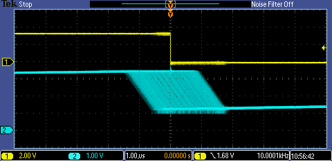
This next trace shows the initial reaction of the phase comparator when the frequency of the reference suddenly increases.
Yellow is the reference signal, blue is the 'up' output from the FPGA. Because the up output only drives high and is tristate at other times, the low part of the waveform reflects the current voltage that's on the filter capacitor. In this initial part of the reaction to the change, the frequencies are a long way apart and the up output is pumping the capacitor frantically to get the two aligned again. The waveform is quite complicated because, although the capacitor waveform is analogue and continuous, this one is kind of discrete time (but with two periods mixed up, one of which is varying; good luck with analysing that: way above my pay grade!). The situation is further complicated because the circuit is a phase lock and not simply a frequency lock, so the phase also needs to be nudged into alignment (by momentarily either speeding up or slowing down the VCO).
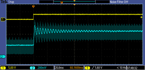
If I look at it that on a longer timescale, I see this. The capacitor voltage has overshot and so then has to be brought back down by the 'down' output from the FPGA.
Here's the down output. This time the output drives to ground with the top of the waveform reflecting the capacitor voltage when the output is tristate.
The up operates over shorter periods than the down because the control voltage is closer to gnd than +3.3V and so the current to pump the capacitor (defined by the resistor in the RC circuit) is less for down than up.
After trying to get the VHDL to work on a iCE40UP-5K part (I failed), I'm now back experimenting with
the filtering. Here's the latest circuit
This settles quicker. This is the step up from 5kHz to 10kHz
This the step down down to 5kHz
The control voltage looks more noisy because the phase comparator can now pull the control voltage
momentarily. The jitter at 10kHz, though, is still about the same
and at 5kHz
is looking more reasonable.
If you want to experiment with the VCO circuit, be aware that there's some mode where the voltage to
current stage can 'latch up' and stop working (the voltage at the 555 timing capacitor sits at about 1V
and doesn't move). Once the oscillator is running it's fine, but sometimes it doesn't start. That seems
to be particularly the case when the FPGA board is powered via the USB and the analogue part only has
the power applied later. I haven't investigated it any further.
Next blog: 555 Frequency Synthesizer
If you found this interesting and would like to see more blogs I've written, a list can be found here: /members-area/b/blog/posts/jc2048-blog-index-new-version
References
[1] https://www.st.com/en/clocks-and-timers/ne555.html
[2] https://www.ti.com/lit/ds/symlink/ne555.pdf
[3] Frequency/Phase Comparator for Phase-locked-Loops. Peter Alfke. Page 6-41, The Programmable Gate Array Data Book, Xilinx, 1989.
Top Comments
-

shabaz
-
Cancel
-
Vote Up
0
Vote Down
-
-
Sign in to reply
-
More
-
Cancel
-

jc2048
in reply to shabaz
-
Cancel
-
Vote Up
0
Vote Down
-
-
Sign in to reply
-
More
-
Cancel
-

shabaz
in reply to jc2048
-
Cancel
-
Vote Up
0
Vote Down
-
-
Sign in to reply
-
More
-
Cancel
-

jc2048
in reply to shabaz
-
Cancel
-
Vote Up
0
Vote Down
-
-
Sign in to reply
-
More
-
Cancel
-

shabaz
in reply to jc2048
-
Cancel
-
Vote Up
0
Vote Down
-
-
Sign in to reply
-
More
-
Cancel
Comment-

shabaz
in reply to jc2048
-
Cancel
-
Vote Up
0
Vote Down
-
-
Sign in to reply
-
More
-
Cancel
Children