


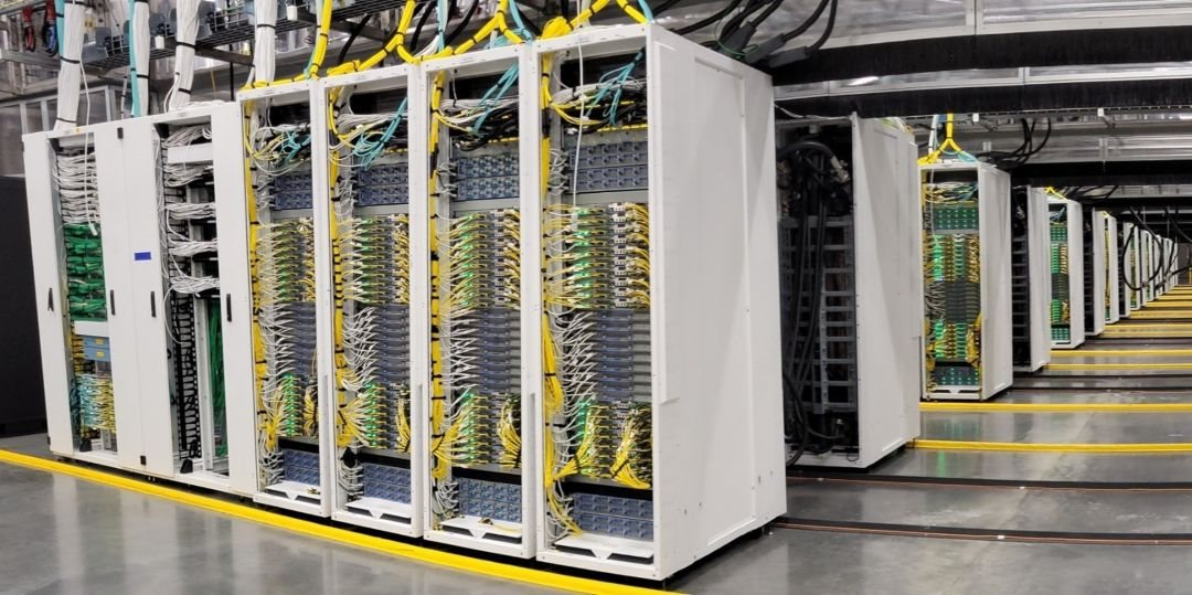
Microsoft’s AI infrastructure servers in a data center. (Image Credit: Microsoft)
AI infrastructure is constantly expanding, and efficiently moving data is as important as processing it. That’s where silicon photonics comes into play for next-gen data centers. According to STMicroelectronics, manufacturing, packaging, and testing photonic devices at scale is the next biggest challenge. To address that, the company is ramping production of its PIC100 silicon photonics platform on 300 mm wafers. STMicroelectronics wants to combine optical performance with the manufacturing scale required for producing photonic chips in large volumes.
Years ago, STMicroelectronics started developing silicon photonics, and this recent push builds on that earlier work. Its PIC25 platform supported 25-GBaud signaling and 50G-per-lane applications. However, the market wasn’t ready for widespread adoption as the technology launched before it had high demand. Building more data centers has changed that due to growing bandwidth requirements exposing copper interconnect limitations.
Although copper works well for short electrical connections, it can struggle to maintain signal quality while controlling power usage when AI systems are scaled. Optical links improve signal integrity, reduce losses, and provide extended range while allowing optical engines to be closer to processors and switch ASICs. The industry is shifting toward near-packaged optics and co-packaged optics. These approaches may create challenges for thermal management, serviceability, and reliability.
The company’s plan involves packaging. To make connections shorter between photonic and electronic components, it is working on through-silicon vias (TSVs) for the silicon photonics and BiCMOS platforms. Additionally, it’s pairing laser drives with packaging technologies like photonic chips, MCUs, and control electronics. This supplies more components essential for optical interconnects.
Usually, the company doesn’t supply AI data centers. Optical module makers and system companies receive photonic and electronic components. These companies then use those parts to develop transceivers and optical engines. For example, Sicoya recently showcased a 1.6T OSFP optical module based on STMicroelectronics’ PIC100 platform. Designed for AI networking, it uses 8 lanes at 200G/lane and combines photonics integrated circuits (PICs) and electronic integrated circuits (EICs).
In addition, Sicoya used die stacking to place the transimpedance amplifier (TIA) atop the PIC, forming shorter connections between the photonic and electronic components. Doing so shortens signal paths and improves integration. With this demonstration, Sicoya showed that optical interconnects don’t just require high performance. Integrating photonic devices, electronics, and packaging them for large-scale production is just as important.
Have a story tip? Message me here at element14.