element14 Community
element14 Community
    Register Log In
  • Site
  • Search
  • Log In Register
  • Community Hub
    Community Hub
    • What's New on element14
    • Feedback and Support
    • Benefits of Membership
    • Personal Blogs
    • Members Area
    • Achievement Levels
  • Learn
    Learn
    • Ask an Expert
    • eBooks
    • element14 presents
    • Learning Center
    • Tech Spotlight
    • STEM Academy
    • Webinars, Training and Events
    • Learning Groups
  • Technologies
    Technologies
    • 3D Printing
    • FPGA
    • Industrial Automation
    • Internet of Things
    • Power & Energy
    • Sensors
    • Technology Groups
  • Challenges & Projects
    Challenges & Projects
    • Design Challenges
    • element14 presents Projects
    • Project14
    • Arduino Projects
    • Raspberry Pi Projects
    • Project Groups
  • Products
    Products
    • Arduino
    • Avnet & Tria Boards Community
    • Dev Tools
    • Manufacturers
    • Multicomp Pro
    • Product Groups
    • Raspberry Pi
    • RoadTests & Reviews
  • About Us
    About the element14 Community
  • Store
    Store
    • Visit Your Store
    • Choose another store...
      • Europe
      •  Austria (German)
      •  Belgium (Dutch, French)
      •  Bulgaria (Bulgarian)
      •  Czech Republic (Czech)
      •  Denmark (Danish)
      •  Estonia (Estonian)
      •  Finland (Finnish)
      •  France (French)
      •  Germany (German)
      •  Hungary (Hungarian)
      •  Ireland
      •  Israel
      •  Italy (Italian)
      •  Latvia (Latvian)
      •  
      •  Lithuania (Lithuanian)
      •  Netherlands (Dutch)
      •  Norway (Norwegian)
      •  Poland (Polish)
      •  Portugal (Portuguese)
      •  Romania (Romanian)
      •  Russia (Russian)
      •  Slovakia (Slovak)
      •  Slovenia (Slovenian)
      •  Spain (Spanish)
      •  Sweden (Swedish)
      •  Switzerland(German, French)
      •  Turkey (Turkish)
      •  United Kingdom
      • Asia Pacific
      •  Australia
      •  China
      •  Hong Kong
      •  India
      •  Japan
      •  Korea (Korean)
      •  Malaysia
      •  New Zealand
      •  Philippines
      •  Singapore
      •  Taiwan
      •  Thailand (Thai)
      •  Vietnam
      • Americas
      •  Brazil (Portuguese)
      •  Canada
      •  Mexico (Spanish)
      •  United States
      Can't find the country/region you're looking for? Visit our export site or find a local distributor.
  • Translate
  • Profile
  • Settings
FPGA
  • Technologies
  • More
FPGA
Blog Learning AMD Zynq: a project to generate a set of PWM signals. 1 - problem statement and possible approach
  • Blog
  • Forum
  • Documents
  • Quiz
  • Events
  • Polls
  • Files
  • Members
  • Mentions
  • Sub-Groups
  • Tags
  • More
  • Cancel
  • New
Join FPGA to participate - click to join for free!
  • Share
  • More
  • Cancel
Group Actions
  • Group RSS
  • More
  • Cancel
Engagement
  • Author Author: Jan Cumps
  • Date Created: 21 Apr 2023 11:42 AM Date Created
  • Views 5042 views
  • Likes 12 likes
  • Comments 36 comments
  • pynq-z2
  • amdzynqultrasoundpulse
  • zynq
  • fpga
  • vivado
  • vhdl
  • pynq
  • spartan
Related
Recommended

Learning AMD Zynq: a project to generate a set of PWM signals. 1 - problem statement and possible approach

Jan Cumps
Jan Cumps
21 Apr 2023
Learning AMD Zynq: a project to generate a set of PWM signals. 1 - problem statement and possible approach

 yepe has to resolve this problem for a project assignment:

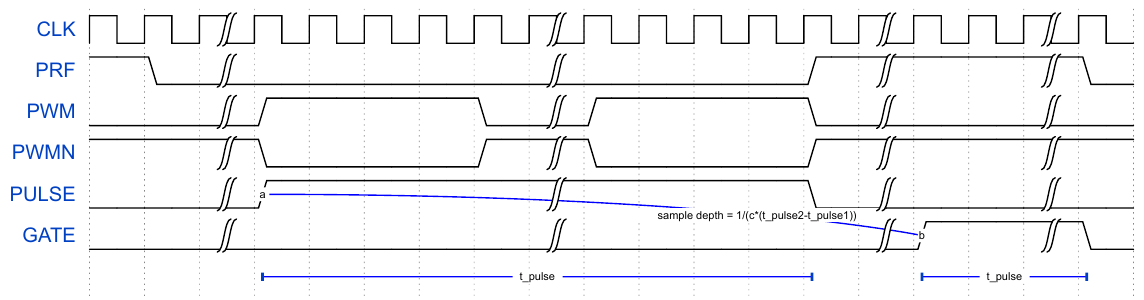
Hi Jan Cumps, I hope you don't mind if I ask a question regarding the PYNQ half-bridge PWM driver. I am working on a student project for school and I need to drive a half-bridge for an ultrasound pulser. I was working through your great tutorial and I had the complementary pwm output on my board PYNQ Z1. However, I have to make certain changes to the operation to make it compatible with my needs which I attempted to do, but I could not determine the best approach. First off, I need to simplify that I only need 50% duty cycle and no other duty cycles needed. I have made a timing diagram for the various waveforms:
image

CLK should be a continuous 20 MHz signal, PRF should be a 10 kHz 50% duty cycle signal that synchronizes the rest of the waveforms. PWM&PWMN are the complementary PWM signals with dead-time of programmable N cycles with a timed delay from a falling edge of PRF. PULSE should be equal to the length of the PWM pulse train, and GATE is equal to pulse but with a programmable delay. The PWM pulse-train should be 5 MHz. The first thing I tried to do is to change your example to see if I could get a 5 MHz complementary PWM but I could not see how the frequency is determined so I was playing around with the board clocks and only could get it up to 650 kHz.

I am a biginner at vhdl so I am a bit out of my element. I have developed all the electronics and analogue demodulation circuits but I still lack the control system to tie it together. If I were to implement these signals in the PYNQ, where do you propose to start?

My suggestion is to cut the task in simple(r) chunks:

I think that the easiest way to achieve this, as beginner, is to eat the elephant in pieces. Ignore my code, because it's not the basis for what you need.

  • make a design that can generate the clock. Confirm by probing.
  • make a design that can generate one of the easy signals, based on that clock. PWM maybe? If you can make that clock, you know that you'll be able to generate the slower ones too (edit jc: the max frequency will a function of the resolution of the dead time).
  • add PWMN to the design. That should be easy, because it's NOT PWM
  • try a separate design with the PRF logic. If you have that working, add to the original one (or keep separate, feeding it from the same clock?)
  • same for the remaining ones.

image

The advantage of little steps is that you'll get early success, and that boosts the morale.
Advantage of separate blocks for a beginner is that the code stays separate and graspable. 

The main job for each signal will will be to:

  • find out after how many ticks of the clock the signal should change
  • count the clock ticks and compare it to the figure(s) figured out above
  • set the output(s) to the desired state.

If you'd handle this different, comment below.

Capture of status after post 2:

image

link to all posts.

  • Sign in to reply

Top Comments

  • michaelkellett
    michaelkellett over 2 years ago in reply to Jan Cumps +1
    Looks to me as if it would be much better with maybe 100MHz internal clock - if the 20MHz is a fixed thing from outside then use an FPGA PLL to get up to 100M (or more). You can get really sassy with…
  • michaelkellett
    michaelkellett over 2 years ago in reply to yepe +1
    Much clearer now - thanks I'll leave Jan to get on with helping (mostly ), otherwise it'll get confusing. MK
  • yepe
    yepe over 2 years ago in reply to Jan Cumps +1
    Hi, sorry for the late response. The delay between the falling edge of the PRF and the beginning of the pulse train should be such that the end of the pulse-train is the same as the end of the low…
  • Jan Cumps
    Jan Cumps over 2 years ago

    To check if things worked, I created a constant for the duty cycle (set to 50%), and a register for the deadband. Now that I got this working, and refreshed my Pynq brain, I made both duty cycle and band a register. You recognise them as the two AXI_GPIO blocks

    image

    In the Jupyter testbed that I created, I can control both values:

    image

    I have set the resolution back to 6 bits for my tests. Because I turned the resolution into a generic in the VHDL code, I can adapt it in the block diagram.

    • Cancel
    • Vote Up 0 Vote Down
    • Sign in to reply
    • More
    • Cancel
  • Jan Cumps
    Jan Cumps over 2 years ago

    With the VHDL PWM from my previous blogs, I can get a 5 MHz differential from a 20MHz clock, if I reduce the resolution to 2 bits.
    There's virtually no wiggle room for deadband then. There are 1 clock pulse left to deal with it.


    To support that, I made the resolution bit width generic:

    --**********************************************************************
    -- Copyright (c) 2011-2014 by XESS Corp <http://www.xess.com>.
    -- All rights reserved.
    --
    -- This library is free software; you can redistribute it and/or
    -- modify it under the terms of the GNU Lesser General Public
    -- License as published by the Free Software Foundation; either
    -- version 3.0 of the License, or (at your option) any later version.
    -- 
    -- This library is distributed in the hope that it will be useful,
    -- but WITHOUT ANY WARRANTY; without even the implied warranty of
    -- MERCHANTABILITY or FITNESS FOR A PARTICULAR PURPOSE.  See the GNU
    -- Lesser General Public License for more details.
    -- 
    -- You should have received a copy of the GNU Lesser General Public
    -- License along with this library.  If not, see 
    -- <http://www.gnu.org/licenses/>.
    --**********************************************************************
    
    --*********************************************************************
    -- Module for generating repetitive pulses.
    --*********************************************************************
    
    library IEEE;
    use IEEE.std_logic_1164.all;
    
    package PulsePckg is
    
      constant HI   : std_logic := '1';
      constant LO   : std_logic := '0';
      constant ONE  : std_logic := '1';
      
    component Pwm is
      generic (
        resolution : integer := 6; -- bit width of the counter used for duty cycle
        duty_bits : integer := 4   -- bit width of the variable that holds the desired deadband 
      );
      port (
        n_reset_i : in  std_logic;          -- async reset
        clk_i  : in  std_logic;             -- Input clock.
        duty_i : in  std_logic_vector (resolution - 1 downto 0);      -- Duty-cycle input.
        band_i : in  std_logic_vector (duty_bits - 1  downto 0);      -- number of clock-ticks to keep both signals low before rising edge
        pwmA_o  : out std_logic;            -- PWM output.
        pwmB_o  : out std_logic             -- PWM output inverse.
        );
    end component;  
    
    end package;
    
    --*********************************************************************
    -- PWM module.
    --*********************************************************************
    
    library IEEE;
    use IEEE.MATH_REAL.all;
    use IEEE.std_logic_1164.all;
    use IEEE.numeric_std.all;
    use WORK.PulsePckg.all;
    
    entity Pwm is
      generic (
        resolution : integer := 6;
        duty_bits : integer := 4
      );
      port (
        n_reset_i : in  std_logic;          -- async reset
        clk_i  : in  std_logic;             -- Input clock.
        duty_i : in  std_logic_vector (resolution - 1 downto 0);      -- Duty-cycle input.
        band_i : in  std_logic_vector (duty_bits - 1 downto 0);      -- number of clock-ticks to keep both signals low before rising edge
        pwmA_o  : out std_logic;            -- PWM output.
        pwmB_o  : out std_logic             -- PWM output inverse.
        );
    end entity;
    
    architecture arch of Pwm is
      signal timer_r       : natural range 0 to 2**duty_i'length-1;
    begin
    
      clocked: process(clk_i, n_reset_i)
      begin
        pwmA_o   <= LO;
        pwmB_o   <= LO;
        
        -- async reset
        if n_reset_i = '0' then
            timer_r <= 0;
            
        elsif rising_edge(clk_i) then
          -- timer
          timer_r <= timer_r + 1;
          -- output a
          if timer_r <= unsigned(duty_i) and timer_r >= unsigned(band_i)  then
            pwmA_o <= HI;
          end if;
          -- output b
          if timer_r > to_integer(unsigned(band_i)) + to_integer(unsigned(duty_i)) then 		
            pwmB_o <= HI;
          end if;
        end if; -- rising_edge
      end process clocked;
      
      
    end architecture;

    I used a clock wizard to generate the 5 MHz:

    image

    I set the resolution to 2 bits in the block diagram:

    image

    Block design:

    image

    Output:

    image

    • Cancel
    • Vote Up 0 Vote Down
    • Sign in to reply
    • More
    • Cancel
  • Jan Cumps
    Jan Cumps over 2 years ago in reply to michaelkellett

    > This doesn't sound like PWM at all.

    I also don't see a dead time in the complimentary signals. They ramp up and down at the same time.
    I hope that by separating the requirements (and the thinking process), each signal's definition could become clearer.

    • Cancel
    • Vote Up 0 Vote Down
    • Sign in to reply
    • More
    • Cancel
  • michaelkellett
    michaelkellett over 2 years ago

    I'm a bit puzzled by the statement:

    "The PWM pulse-train should be 5 MHz."

    And the more I look the more puzzled I am:

    "First off, I need to simplify that I only need 50% duty cycle and no other duty cycles needed"

    This doesn't sound like PWM at all.

    I think it's more that yepe wants to drive a half bridge at 5MHz, but his diagram shows all the "PWM" pulses driving in the same direction.

    At this point I'm feeling I want to look at the whole menu again before I order the elephant sandwich.

    Or, rather, see a schematic of the half bridge and its load.

    MK

    • Cancel
    • Vote Up 0 Vote Down
    • Sign in to reply
    • More
    • Cancel
  • shabaz
    shabaz over 2 years ago

    The PRF signal sounded interesting, I couldn't tell if it is internally generated, or externally generated since they mention having to sync to it. If it's external then that might need a PLL. A block diagram showing all signals would also helps that they can implement it in chunks as you recommended. Maybe this is a uni project, in which case if it is a team project and they must have worked on some sort of diagrams of the system to share the work, but hasn't been shared.

    • Cancel
    • Vote Up 0 Vote Down
    • Sign in to reply
    • More
    • Cancel
<>
element14 Community

element14 is the first online community specifically for engineers. Connect with your peers and get expert answers to your questions.

  • Members
  • Learn
  • Technologies
  • Challenges & Projects
  • Products
  • Store
  • About Us
  • Feedback & Support
  • FAQs
  • Terms of Use
  • Privacy Policy
  • Legal and Copyright Notices
  • Sitemap
  • Cookies

An Avnet Company © 2026 Premier Farnell Limited. All Rights Reserved.

Premier Farnell Ltd, registered in England and Wales (no 00876412), registered office: Farnell House, Forge Lane, Leeds LS12 2NE.

ICP 备案号 10220084.

Follow element14

  • X
  • Facebook
  • linkedin
  • YouTube