


Table of Contents
Introduction
The recent releases of KiCad support built-in SPICE simulation.
I was busy working on a schematic to ultimately convert into a printed circuit board for a new measurement amplifier version 4 (here is version 3), but while I was at it, I wished to simulate it. It was possible to steer the schematic toward that purpose very easily!
This blog post shows how to (at least minimally) get going with simulation.
If you want to play along, you can download a zip file containing the KiCad project discussed here and try it out! I’m using KiCad 8.0. The end result will be converted into a real circuit, so any contributions will be welcome.
If you're totally new to KiCad, you may want to view a YouTube 50-minute KiCad course.
Create the Schematic
The schematic for simulation is created just as if you were creating a schematic for PCB design. You use the same component symbols. Nothing is different. Here’s my circuit (it’s actually more of a sub-circuit because I have not completed it! This is just the gain stage sub-circuit for a larger project, which will be a measurement amplifier):
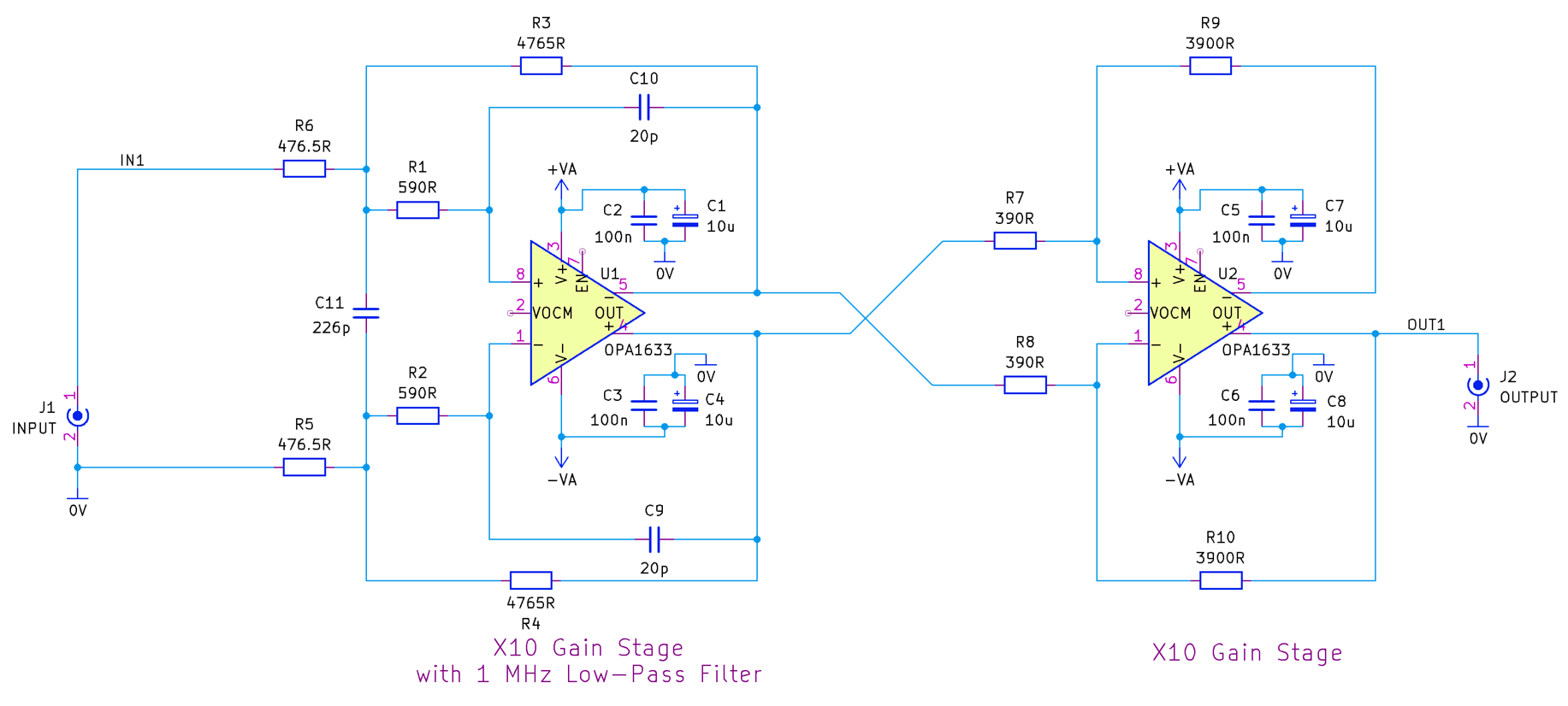
As you can see, it looks like any other schematic. I used regular component symbols. A key thing is to label your inputs and outputs (press the L key to add labels). It will work without labels, but adding labels will make the signals easier to locate in the end simulation results.
Adding SPICE models
The resistors and capacitors in the above circuit have built-in ideal component SPICE models, and they can be ignored (generally!). However, the circuit contains two OPA1633 op-amps and two coaxial connectors (J1 and J2). The simulation needs to know what to do with these components.
The connectors are easy to deal with. Open the connector symbol in the KiCad Symbol Editor, and then click on File->Symbol Properties. In the pop-up window that appears, click on Simulation Model at the bottom of the window. I chose a built-in SPICE model, namely that of a capacitor, and set it to 1e-14 Farads, i.e., 0.01 pF. That’s it!

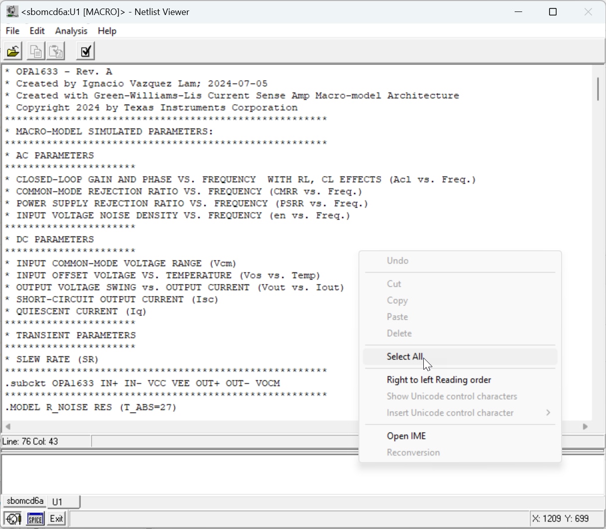
Next, the OPA1633 needs a SPICE model. I went to the manufacturer's website (Texas Instruments, and looked for a SPICE file. I didn’t find it, so I resorted to downloading whatever model they had, which was a Tina-TI schematic file (.tsc suffix). Within the Tina-TI software, it is possible to double-click on the op-amp symbol in the opened schematic and then click on Enter Macro. You’ll now see the SPICE model. Right-click and select all, and then copy it to the clipboard. Paste it into an empty file, and save it with the filename opa1633.lib in the folder C:\Users\myusername\Documents\KiCad\8.0\simulation (modify that path to suit your system).
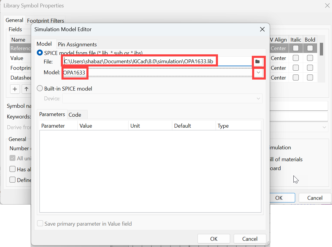
Next, open the symbol in the Symbol Editor in KiCad (there isn’t an OPA1633 symbol in KiCad by default, but I’m assuming you already know how to create new symbols since that’s core to general schematic entry; it is covered in the 50-minute KiCad training video mentioned earlier), and then, as before, click on File->Symbol Properties and then click on Simulation Model. This time, select SPICE model from file, and then click on the file icon and select the SPICE model lib file. In the Model row, click on the drop-down chevron and select OPA1633 (this is derived from the content in the SPICE model file). Don’t click on OK yet; keep the window open for the next part.
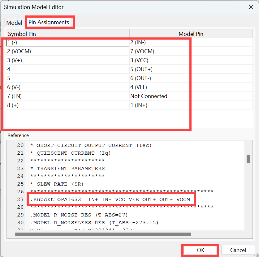
This next part is the trickiest bit. The aim is to tell the simulation software how to map the nodes in the SPICE model, to the pin numbers in the graphical symbol. Click on Pin Assignments. Take a look at the SPICE model text, and look for the .subckt OPA1633 line. The SPICE model connection names are listed there. You need to map those names (under Model Pin in the table) to the connection names in the graphical symbol (incidentally, the numbers against each name in the Model Pin list can be ignored; that's the sequence number for the entries on the .subckt OPA1633 line). Once that’s done, click on OK.
Adding Simulation Voltages
The schematic requires simulated voltages for power supplies and for stimulus. These are added into the schematic using the normal add component dialog (i.e. press ‘A’ to add a component), and using the Simulation_SPICE library.
I used the component called VDC to simulate the DC power supply. My circuit needs two power rails, so there are two VDC components, set to 7V. You’ll also need a GND component from that same library, you can see in the screenshot below how I attached it to my 0V rail.
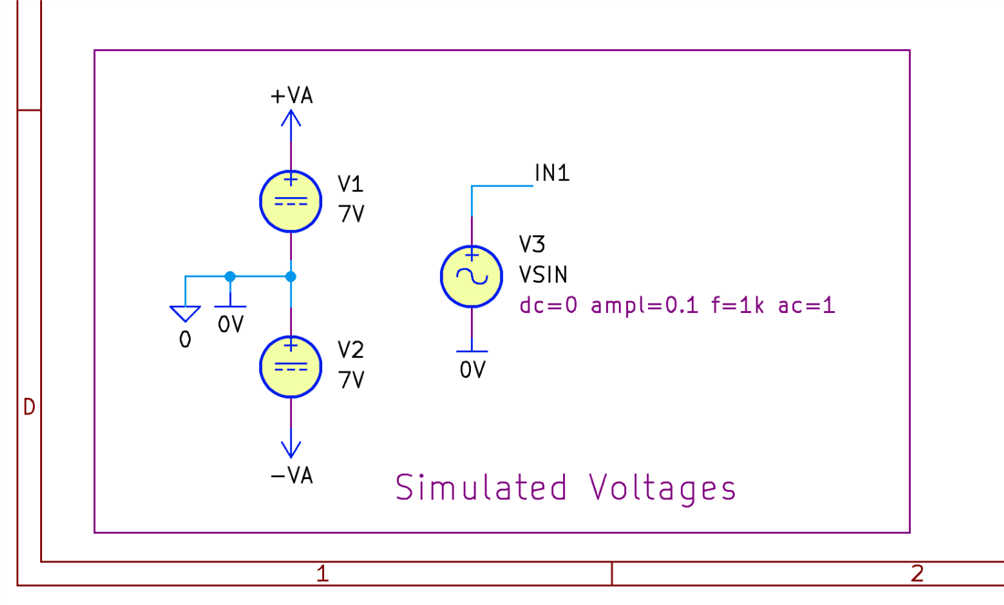
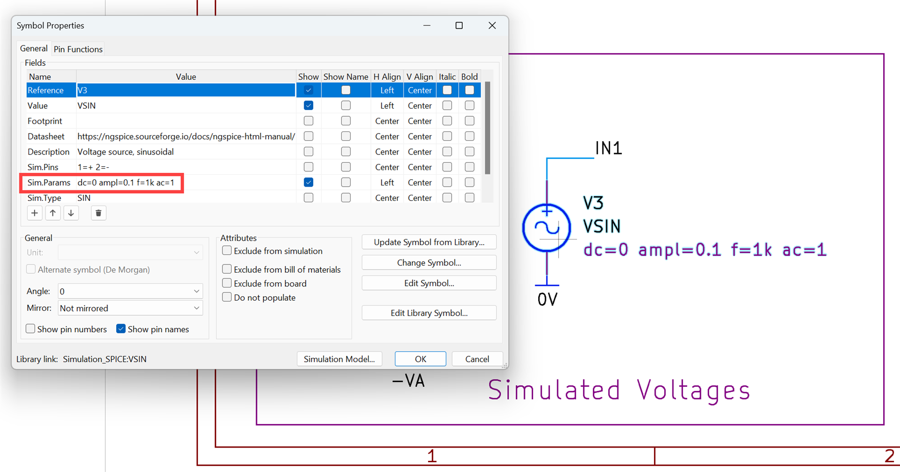
The circuit is an amplifier, and I wanted to test with a sine wave. That requires a VSIN component.
You’ll need to set the amplitude and frequency. This is achieved by editing a string as shown below. This is a bit clunky (because it has its roots in SPICE, but deserves a proper menu). Anyway, as you can see, I’ve set an amplitude of 0.1 V, and a frequency of 1 kHz.
Now you’re ready to simulate!
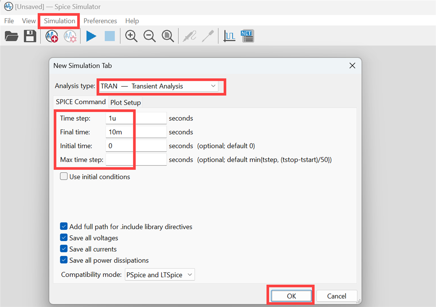
Running a Simulation
From the Schematic Editor, click on Inspect->Simulator. Next, click on Simulation->New Analysis Tab (or just press the triangular Run icon). A New Simulation window appears. The most common/basic simulation is probably Transient Analysis, TRAN, which shows an output that looks like an oscilloscope view. The screenshot below shows how it is configured. I decided that I wanted SPICE to compute an output every microsecond, for a total of 10 msec.
When you click on OK, the simulation will run, and a blank chart area will appear. Signals will be listed on the right. Locate in the list, the signal names corresponding to the labels that were in the schematic (I called them IN1 and IN2), they should be near the top of the list, and click in the adjacent boxes to enable the plotted output!
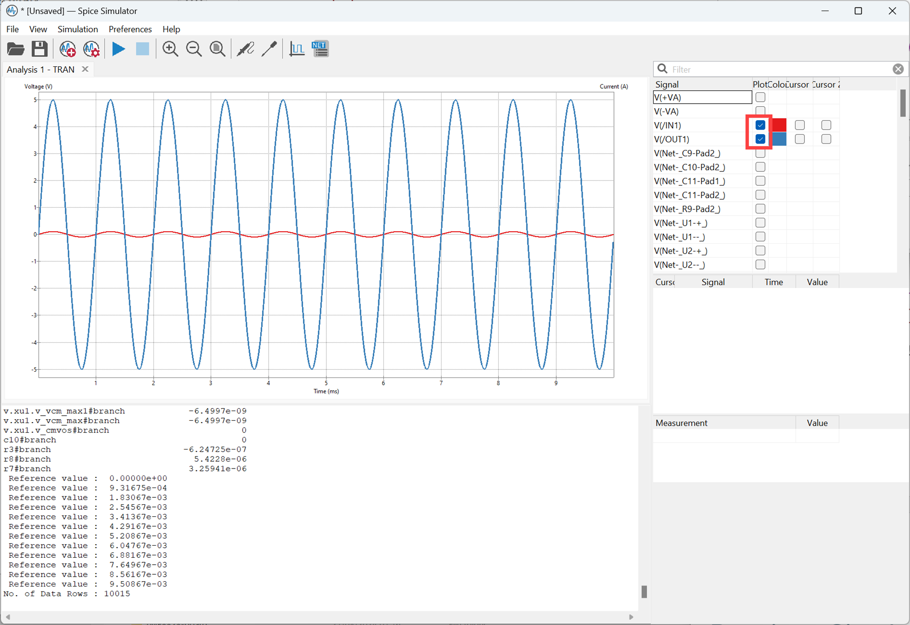
To improve the display, click on View->Dark Mode Plots to disable it, to make the background white (if it was originally black). Also, click on View->Show Legend to display a color key legend on the chart. The text is all quite tiny, I don’t know of a way to increase the size within KiCad.
I also don’t know of a way to enable cursors on the chart. Fortunately, it is possible to save the output in CSV format (click on File->Export Current Plot as CSV) and examine the data using other tools (such as Matlab or Python).

Plotting Frequency Response
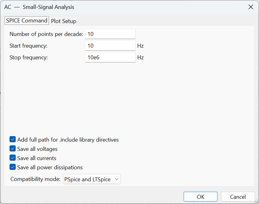
The frequency response can be plotted by running a different simulation. As before, in the simulation window, click on Simulation->New Analysis Tab and this time choose AC instead of TRAN. Populate the boxes with sensible values (in the screenshot below, you can see that I was interested in the frequency response between 10 Hz and 10 MHz.
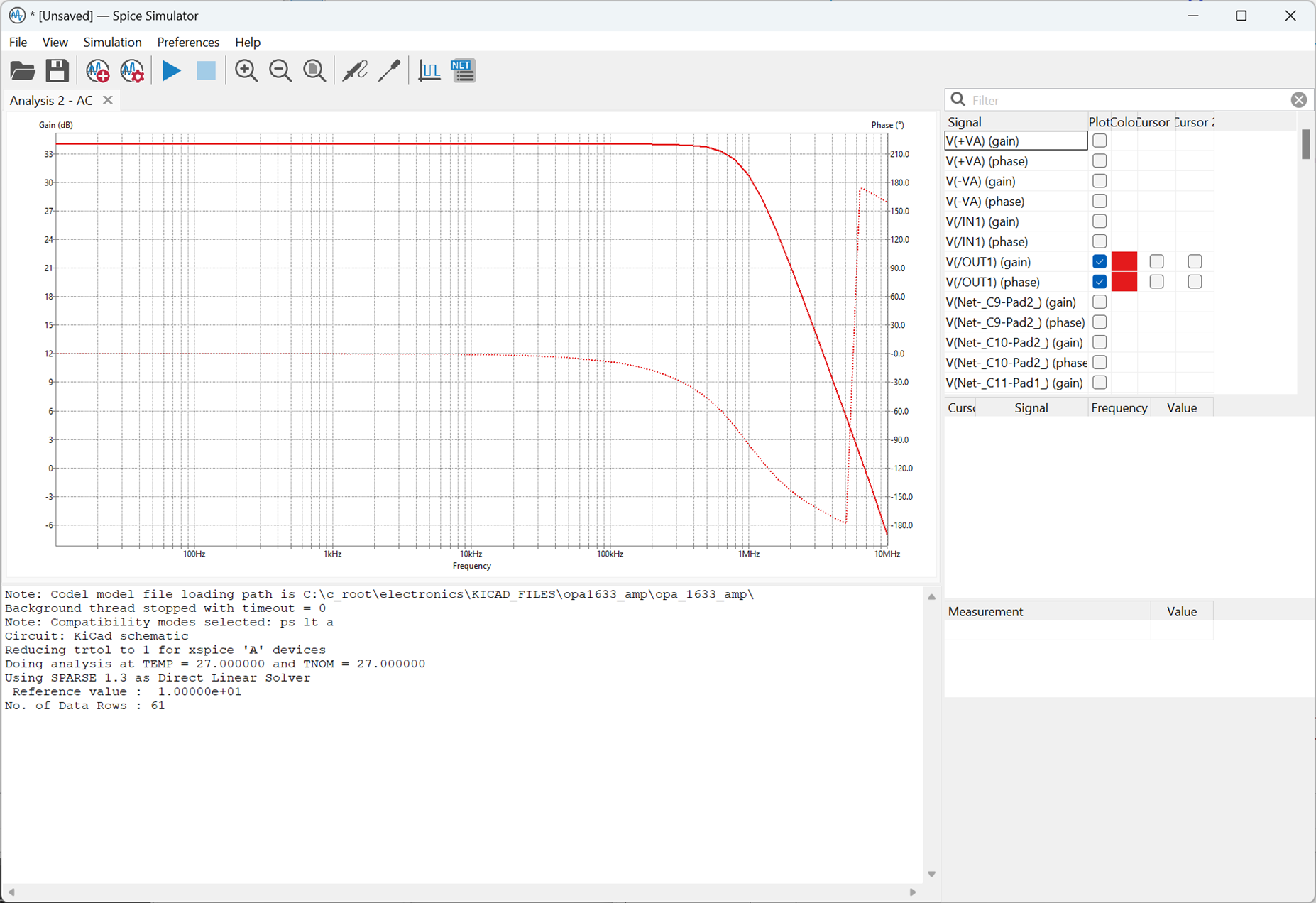
Click OK, and then click on the Run Simulation triangle. Then, select the signal of interest in the list on the right. A chart should appear!
Simulating Parts of a Circuit (Excluding some Components)
With KiCad 8, you can selectively disable some components from the simulation, by selecting a portion of circuit, then right-clicking and selecting Attributes->Exclude From Simulation.
Personally I think this is not easy to work with. A solution proposed here of sorts, is to split your circuit into separate sheets in a hierarchy, and ensure that the portions that you wish to simulate, and the portions that you do not wish to simulate, are on separate sheets. You could for instance have five sheets, where one sheet is never simulated, and the other four sheets are simulated independently.
Then, you need a way to set the Exclude from Simulation attribute on a per-sheet basis. This is currently not possible from KiCad, however there is a Python program called sim_select.py (idea by Jan Cumps ) that can do this. It will prompt the user which sheet is desired to be simulated, and it will set the attributes of all sheets accordingly.

Summary
Schematics ready for simulation are created within KiCad by assigning a SPICE model to components, and then adding voltage sources and stimulus signals from the Simulation_SPICE component library. You can find SPICE model files from electronic component manufacturer websites. Don’t forget to label your inputs/outputs.
When you bring up the Simulation window (using Inspect->Simulator), you can select a Transient Analysis, which is simplest to understand, and instruct it to compute currents and voltages at granular intervals, for a period of time. A chart of voltages can be easily plotted, that looks similar to what would be seen with an oscilloscope connected to a real circuit.
The KiCad project file can be downloaded if you wish to experiment with simulations.
If you manage to run any interesting simulations, please share the results! The KiCad project zip file is for a real circuit I intend to make and needs improving (it needs an input buffer and an output buffer that converts from differential to single-ended output), plus configurable filtering, plus the ability to high-pass-filter the input to block DC optionally. If you do give it an attempt, or even if you don't, I would appreciate any suggestions/circuit additions.
Thanks for reading!
Top Comments
-

shabaz
-
Cancel
-
Vote Up
0
Vote Down
-
-
Sign in to reply
-
More
-
Cancel
-

Jan Cumps
in reply to shabaz
-
Cancel
-
Vote Up
0
Vote Down
-
-
Sign in to reply
-
More
-
Cancel
-

shabaz
in reply to Jan Cumps
-
Cancel
-
Vote Up
0
Vote Down
-
-
Sign in to reply
-
More
-
Cancel
-

Jan Cumps
in reply to shabaz
-
Cancel
-
Vote Up
0
Vote Down
-
-
Sign in to reply
-
More
-
Cancel
-

shabaz
in reply to Jan Cumps
-
Cancel
-
Vote Up
0
Vote Down
-
-
Sign in to reply
-
More
-
Cancel
Comment-

shabaz
in reply to Jan Cumps
-
Cancel
-
Vote Up
0
Vote Down
-
-
Sign in to reply
-
More
-
Cancel
Children