element14 Community
element14 Community
    Register Log In
  • Site
  • Search
  • Log In Register
  • Community Hub
    Community Hub
    • What's New on element14
    • Feedback and Support
    • Benefits of Membership
    • Personal Blogs
    • Members Area
    • Achievement Levels
  • Learn
    Learn
    • Ask an Expert
    • eBooks
    • element14 presents
    • Learning Center
    • Tech Spotlight
    • STEM Academy
    • Webinars, Training and Events
    • Learning Groups
  • Technologies
    Technologies
    • 3D Printing
    • FPGA
    • Industrial Automation
    • Internet of Things
    • Power & Energy
    • Sensors
    • Technology Groups
  • Challenges & Projects
    Challenges & Projects
    • Design Challenges
    • element14 presents Projects
    • Project14
    • Arduino Projects
    • Raspberry Pi Projects
    • Project Groups
  • Products
    Products
    • Arduino
    • Avnet & Tria Boards Community
    • Dev Tools
    • Manufacturers
    • Multicomp Pro
    • Product Groups
    • Raspberry Pi
    • RoadTests & Reviews
  • About Us
    About the element14 Community
  • Store
    Store
    • Visit Your Store
    • Choose another store...
      • Europe
      •  Austria (German)
      •  Belgium (Dutch, French)
      •  Bulgaria (Bulgarian)
      •  Czech Republic (Czech)
      •  Denmark (Danish)
      •  Estonia (Estonian)
      •  Finland (Finnish)
      •  France (French)
      •  Germany (German)
      •  Hungary (Hungarian)
      •  Ireland
      •  Israel
      •  Italy (Italian)
      •  Latvia (Latvian)
      •  
      •  Lithuania (Lithuanian)
      •  Netherlands (Dutch)
      •  Norway (Norwegian)
      •  Poland (Polish)
      •  Portugal (Portuguese)
      •  Romania (Romanian)
      •  Russia (Russian)
      •  Slovakia (Slovak)
      •  Slovenia (Slovenian)
      •  Spain (Spanish)
      •  Sweden (Swedish)
      •  Switzerland(German, French)
      •  Turkey (Turkish)
      •  United Kingdom
      • Asia Pacific
      •  Australia
      •  China
      •  Hong Kong
      •  India
      •  Japan
      •  Korea (Korean)
      •  Malaysia
      •  New Zealand
      •  Philippines
      •  Singapore
      •  Taiwan
      •  Thailand (Thai)
      •  Vietnam
      • Americas
      •  Brazil (Portuguese)
      •  Canada
      •  Mexico (Spanish)
      •  United States
      Can't find the country/region you're looking for? Visit our export site or find a local distributor.
  • Translate
  • Profile
  • Settings
Open Source Hardware
  • Technologies
  • More
Open Source Hardware
Blog Simple DCR (Direct Conversion Receiver) – Part 2: Common Emitter Amplifier
  • Blog
  • Forum
  • Documents
  • Events
  • Polls
  • Members
  • Mentions
  • Sub-Groups
  • Tags
  • More
  • Cancel
  • New
Join Open Source Hardware to participate - click to join for free!
  • Share
  • More
  • Cancel
Group Actions
  • Group RSS
  • More
  • Cancel
Engagement
  • Author Author: shabaz
  • Date Created: 24 Mar 2026 3:06 AM Date Created
  • Views 277 views
  • Likes 10 likes
  • Comments 15 comments
  • 7MHz
  • 40m
  • simple_dcr
  • hf
  • radio
  • rf
  • amateur radio
Related
Recommended

Simple DCR (Direct Conversion Receiver) – Part 2: Common Emitter Amplifier

shabaz
shabaz
24 Mar 2026

Table of Contents

  • Introduction
  • Circuit Diagram
  • Dealing with Inputs and Outputs
  • Power Supply Problem!
  • Applying a Signal
  • Frequency Response
  • Loading the Amplifier
  • Testing Both Stages Together
  • Summary

For all blog posts in this series, click here, or type simple_dcr in the search box at the top of this page!

Introduction

This blog post is about a fairly popular, low-cost, easy-to-build radio receiver project, intended for speech and tones (not music) on radio channels at approximately 7 MHz. You need a radio license to transmit in the 7 MHz amateur radio band, but it’s legal for anyone to construct a receiver and listen to that band.

I decided to create a printed circuit board (PCB) and assemble the circuit.

In the first blog post, I started construction back-to-front, at the very last part of the audio power amplifier stage that connects to an 8-ohm speaker, and determined that the stage works best with an audio input limited to a ballpark of about 40-80 mV p-p, depending on how much distortion one is willing to tolerate. Beyond 80 mV p-p, the distortion is very bad.

In this blog post, I decided to continue working back-to-front and assemble the amplifier stage immediately preceding the final stage assembled in the last blog.
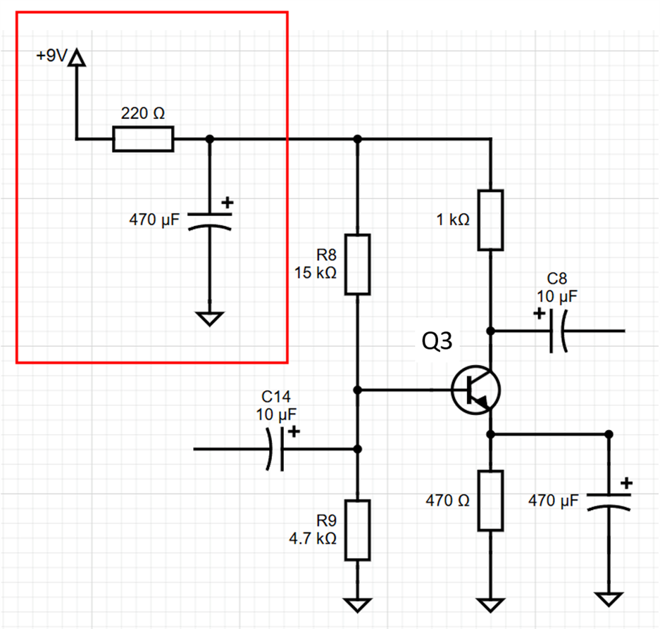
Circuit Diagram

The green portion of the circuit was constructed and tested in blog #1. For this blog 2, the blue portion was assembled. Also, the capacitor C8 was temporarily disconnected at the spot marked with X, so that the blue stage could be tested in isolation.

image

Dealing with Inputs and Outputs

Usually, one uses oscilloscope probes to view signals in a circuit under test. Sometimes I use a thin coax cable instead. It’s not recommended, but you can get away with it for some tests, especially at very low frequencies, such as for audio amplifiers. Where a coax cable becomes important is for delivering signals from a signal generator or for viewing signals at higher frequencies, provided that the cable end has a 50-ohm termination.

In any case, I used coax cables with small SMA connectors on the ends, because SMA sockets can be low-cost, and are easy to solder onto a PCB with short lengths of wire, but you could use proper oscilloscope probes as recommended.

Power Supply Problem!

For initial testing, I shorted the input of the audio amplifier (actually, I just attached an SMA attenuator because it was close at hand; that’s almost a short), and then probed the output at the output capacitor, with the last stage disconnected at the spot labelled X as discussed earlier.

You’d expect to see a flat line on the ‘scope, close to 0V (or 0V if you’ve set the oscilloscope to AC input).

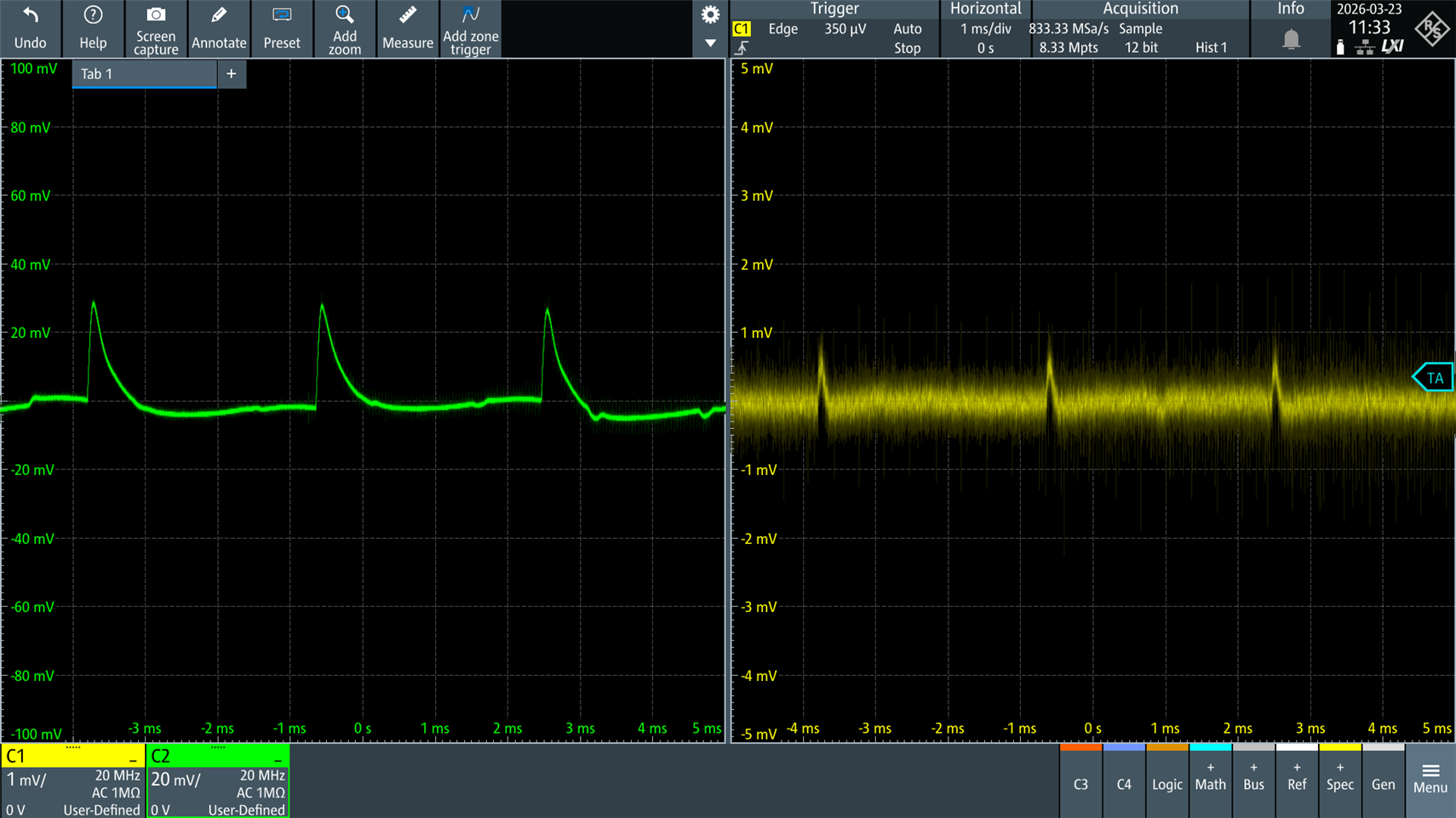
The project is intended to run from a nominal 9V supply, specifically a 9V battery. For testing, I was using a bench power supply that had an unfortunate fault: approximately 30 mV amplitude pulses at about 300 Hz (I don’t know why; I’ll open it up sometime). The power supply pulses are shown in green in the screenshot below.

The yellow trace is the amplifier stage output! It’s unusable, since if the expected output from the amplifier stage is to be about 40mV p-p, the pulses are of a similar ballpark amplitude; it would completely destroy the signal-to-noise ratio for the desired signal!

The problem occurs because the amplifier is not very good at rejecting power supply ripple. Ordinarily, this might be unnoticeable when powered by a 9V battery, but as soon as you connect any realistic power supply, the noise on the supply rail will swamp the output, because all typical power supplies have noise. The problem will be even worse for the amplifier stage that will be built in blog 3, since that stage handles even lower-amplitude signals at its input, but I’ll cross that bridge when I come to it. If you have any suggestions, please let me know! (ideally in-tune with the circuit philosophy, which is discrete parts; perhaps I need a Zener supply? The amplifier stage's current consumption will be just a few milliamperes.

image

One solution is to decouple the supply using some filtering. To do that, I disconnected the two resistors from the 9V supply rail, and inserted a resistor and capacitor as shown in the red box. Apologies for the poor circuit diagram; my PC was missing KiCad.

image

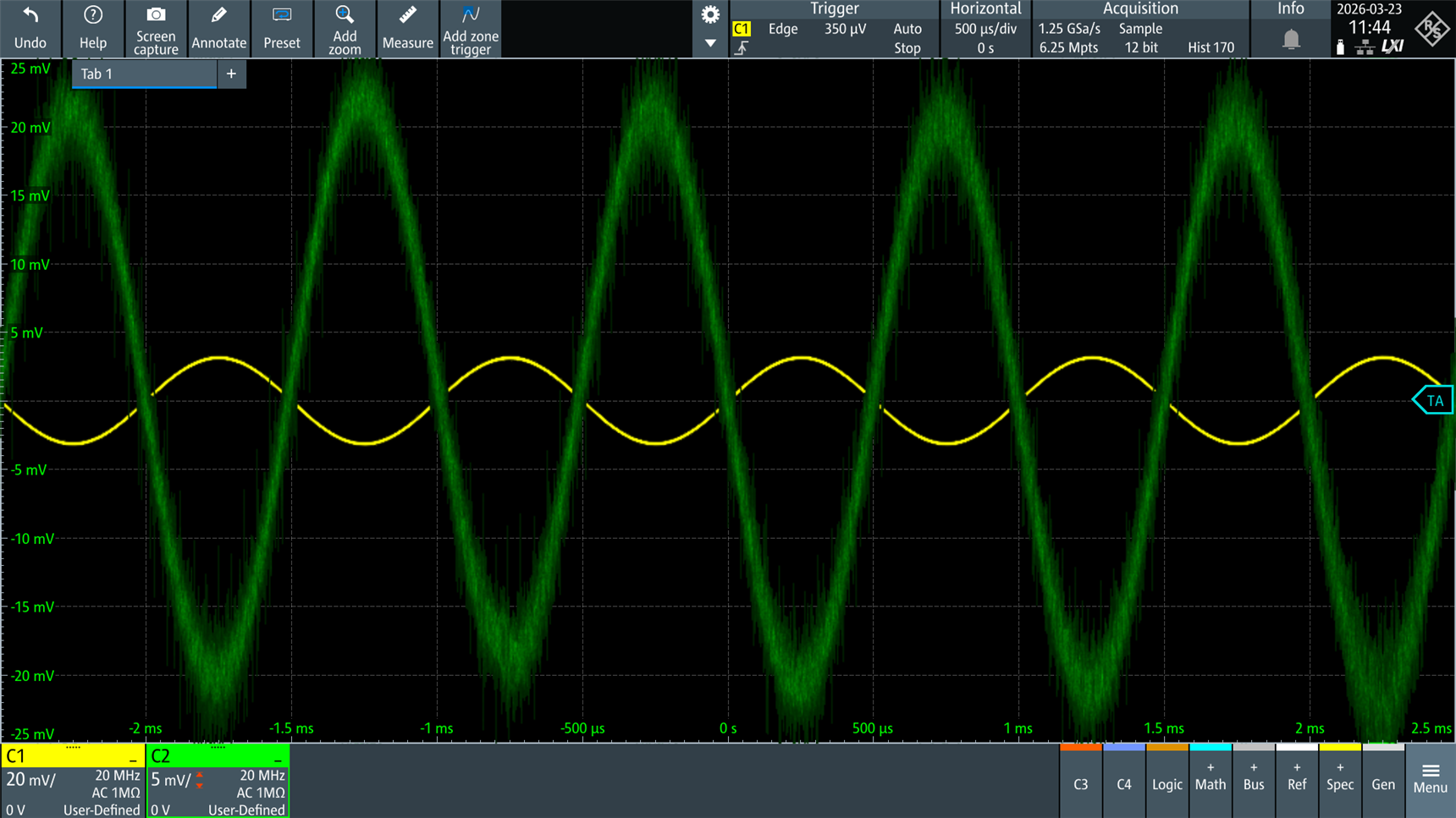
Now the result was usable. As can be seen, the 30 mV PSU spikes (green) are now just 1 mV spikes (yellow). Hopefully, most typical power supplies will have a bit less noise than my faulty PSU.

image

To summarize, the main takeaway is that such basic amplifiers need a stable power supply, especially when the output signal is expected to be low amplitude, and at a minimum, it could be a resistor and capacitor filter in the supply rail to the amplifier.

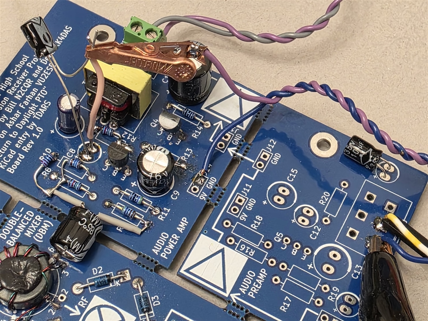
The photo here shows the extra resistor and capacitor bodged onto the PCB. The alligator clip attaches to the amplifier's output (the negative lead of capacitor C8), and the pink wire next to it is used to reconnect the amplifier to the next stage when required. The amplifier input is lower-right in the photo (where the potentiometer would normally go).

image

Applying a Signal

Now that the power supply problem was not as much of an issue, I decided to apply a sine-wave input to the amplifier. Here, there’s a test equipment-related issue to overcome: the amplifier has a gain of approximately 95, so for a desired output of 40 mV p-p (to avoid overdriving the final amplifier stage), the input signal needs to be about 0.4 mV p-p.

Typical signal generators cannot create such low-amplitude signals. I decided to attach some SMA attenuators in line to drop the amplitude a bit. It’s worth having a few attenuators on hand if you’re working with signal generators; you can DIY them too.

Decent attenuators cost a fair bit, but for very non-critical work, there are AliExpress options (this is definitely not advised for real work, because a failure would be very easy to miss, would be extremely easy to occur, and there’s a high chance it could destroy test equipment or circuitry under test, when working with higher power sources). Plus, even when functioning, they likely won’t meet the advertised specs, especially at higher frequencies. If you’re purchasing for work purposes, they absolutely need to be known brand attenuators from a distributor.

image

I applied a signal, added attenuators as required, and adjusted the signal generator output so the green output was about 40 mV p-p. The yellow signal shows the signal generator output, but the amplifier input was connected to an attenuated version of that, therefore the displayed amplitude of the yellow trace can be disregarded; the amplifier gain is about 95, so the attenuated input will have been approximately 400 uV p-p.

image

Frequency Response

The screenshot below shows the frequency response in blue over the range of 100 Hz to 10 kHz; as can be seen, it’s essentially flat. The dB value on the left is not relevant, since the signal at the amplifier input was attenuated, as mentioned earlier, whereas the oscilloscope was attached directly to the unattenuated signal.

image

Loading the Amplifier

So far, the amplifier had been tested in isolation, with capacitor C8 temporarily disconnected from the final power amplifier stage. Next, C8 was reconnected, and the frequency response was measured again at the same point in the circuit. It can be seen that the output drops with that load, reducing from the 4 dB shown in the response chart above, down to -1 dB (i.e. a 5 dB difference, which is about half the amplitude) at 100 Hz, and then falling to about – 6 dB (a 10 dB difference from the unloaded response, i.e. the output is about a third of the unloaded amplitude) by 1 kHz.

image

While the non-flat loaded response isn’t great, it’s probably not that big a deal for speech and tones.

Testing Both Stages Together

From the first blog post, we know that the final audio amplifier stage requires about 40 mV p-p before the speaker output distorts.

The amplifier stage discussed in this blog has its amplitude drop to about a third to a half as it gets loaded by the final stage, therefore the input needs to be driven to about 2 mV p-p to drive the final stage to a comfortable level.

The screenshot below shows the 2 mV p-p input in green, and the output across an 8-ohm load attached to the final stage is shown in white.

image

Here’s the frequency response (ignore the dB value, since I again used an attenuator, whereas the frequency response chart uses the direct signal generator output). While not perfect, I think it’s very acceptable for speech and tones:

image

The proof is in the pudding, so I attached a real 8-ohm speaker (rather than the 8-ohm resistor I had been using) and connected the input to an audio source. The video here shows the audio input signal; a little overdriven as you can see from the amplitude, but as you can hear, the audio is still very intelligible – and loud enough for such a basic amplifier. There is audible fan noise in the recording, picked up by the microphone; that's from the nearby power supply.

You don't have permission to edit metadata of this video.
Edit media
x
image
Upload Preview
image

Summary

A common-emitter amplifier was constructed, but the poor power-supply rejection ratio needed to be improved to prevent supply noise from swamping the low-amplitude signal. An RC filter was used to decouple the supply, and it greatly improved the output.

The frequency response isn’t flat once the amplifier is loaded with the final amplifier stage, but the overall audio can still sound reasonably intelligible, even with a bit of distortion when the input is slightly overdriven.

The combined amplifiers from this blog and blog 1 require an input signal of several millivolts peak-to-peak to produce usable volume from the 8-ohm speaker at an acceptable level of distortion. Eventually, the audio amplifier will get replaced with a better design, but for now, it’s usable.

The next step is to build the first audio amplifier stage (based around transistor Q5 in the circuit in blog 1), and try to improve the power supply rejection significantly, since it’s more critical the smaller the amplitude of wanted signals there are.

Thanks for reading!

  • Sign in to reply
  • shabaz
    shabaz 1 day ago in reply to michaelkellett

    Nice audio analyzer! I'm fairly sure I used that model at a place where they developed radio receivers/transceivers.

    Thanks for the power amp circuit too, I'll work on that PCB this week. I've updated the DC coupled pair schematic/PCB, and now also added SPICE simulation into the schematic. For anyone wishing to use SPICE with their KiCad projects: It's a bit tricky to create a schematic that can be both simulated and converted into a PCB. One trick is to link the SPICE 0 volt symbol to 0V/GND whatever using a very low resistance (and mark that resistor as absent from the board and BoM). If you don't do that, any ground fills won't work because the ground net is swallowed up and gets replaced with the SPICE 0 net.

    Also, simulation will not be possible if the schematic includes non-SPICE parts like connectors etc. The official solution is to mark those connector components as non-simulation, however that has the side-effect that the schematic shows an ugly box around them. A better solution (in my opinion) is to create a "fake" SPICE model for the connectors - I just pretended there was a very high resistance between the connector pins. Anyway, long story short, by using these two techniques, the SPICE stuff is benign when creating the PCB from the schematic, and yet it successfully simulates too.

    image

    • Cancel
    • Vote Up 0 Vote Down
    • Sign in to reply
    • More
    • Cancel
  • michaelkellett
    michaelkellett 2 days ago in reply to shabaz

    I've done some measuring on the pre-amp and the power amp.

    I used an HP8903B Audio Analyzer. It combines sig gen and distortion measuring in one box. The sign gen can do 1mV min which isn't as low as we would like for this. I have an older HP signal generator that can do better (it has a built in 100dB attenuator with 1dB steps) but the matched impedance stuff is a nuisance.

    Using the 8903B I measured the preamp with the 1k load, 8V supply.

    At 1kHz 1mV in gives 0.173V out = gain of 173 = 44.76dB - same as I measured with different gear on 28/03/2028 and as you would expect from calculation.

    The simulation predicts 44.95dB so I'm happy with that.

    The THD at that level is 0.36% and SINAD (noise and distortion) = 48.8dB

    Increasing the input gives 0.92% THD at 2mV and 2.7% at 2.5mV where the output is beginning to clip.

    I increased the load to 4k7 which gives distortion of 1.04% for 5.8mV in and 1.019V out. At 2mV input the distortion was 0.12% and SINAD = 58dB.

    I used a 22k log pot (only one I had) for the volume control and it works fine.

    I connected the power amp I described in your other radio blog and used it to drive speaker (rather a big one but I had nothing smaller readily to hand).

    I could get about 1.66V at the visible (on the scope) onset of clipping.

    At 1.5V (about 280mW into 8 ohms) output the distortion was 0.52% and SINAD 45dB.

    A figure that used to be quoted in HiFi circles for integrated amplifiers (ie those with pre amps and power amp in one box) was "Overload Margin". It's the maximum signal you can apply to the input before clipping or other bad effect at the input to the volume control, compared with the signal for full power output with the volume at max.

    In the case of this pre-amp and power amp combo it's not ideal - the preamp overloads with about 5x nominal input signal level for an overload margin of only 14dB. With radio I think 20dB is the least one should aim for and 30dB would be better.

    This could be achieved by reducing the gain of the pre-amp and increasing the gain of the power amp.

    The power amp can cope with R5 being reduced to 100R (although ideally you would then increase C2 to 22uF.

    If you increase R9 to increase the gain you will need to reduce C4 and increase R6 an R13 to keep the DC bias resistance on the bases of Q1 and Q6 balanced.

    Then you will possibly (probably) need to reduce the gain of the pre-amp because we have increased the gain of the power amp by 20dB.

    This will increase the overload margin to 34dB.

    Since this tuning is all just component values I suggest you see how it feels when you build the first one !

    Power amp design

    image

    HP Audio Analyzer 8903B

    image

    Pre amp and power amp

    image

    MK

    • Cancel
    • Vote Up 0 Vote Down
    • Sign in to reply
    • More
    • Cancel
  • shabaz
    shabaz 2 days ago in reply to michaelkellett

    Thanks for the info! I'll get the capacitor added.

    • Cancel
    • Vote Up 0 Vote Down
    • Sign in to reply
    • More
    • Cancel
  • michaelkellett
    michaelkellett 2 days ago in reply to shabaz

    Since I last posted I've built the DC coupled pair on veroboard and found I needed a 220pF cap base-collector of Q2 to make the amp stable.

    The simulation is fine without but in real life it oscillates .

    I may get time today to blog about testing it (and the power amp) but you should certainly add the 220pF to your board.

    It's also occurred to me that the vol control pot might be much better at 5k or 10k - I shall try that later.

    This is my current veroboard circuit - some of the tweaks are because I didn't have any 10uF caps with leads (or the right transistors) !

    (I have since updated my stock of cheapo electrolytics)

    I'll look forward to seeing the boards - thanks.

    image

    MK

    • Cancel
    • Vote Up 0 Vote Down
    • Sign in to reply
    • More
    • Cancel
  • shabaz
    shabaz 3 days ago in reply to michaelkellett

    Hi Michael,

    I've placed your two preamp designs into KiCad, and created PCB layouts, so that both designs can be tried out. The boards are 40x40mm, I did try to take care not to cause any feedback, not sure how successful I was, and there is an almost full ground plane on top. I've not placed the PCB order yet (working on another project, so I will include these in the same order) but will send you a board too when they arrive. All the files (KiCad 10, plus PDF etc), plus Gerber files are in Github.

    For the off-board connections, the audio inputs/outputs can either be 3.5 mm audio connectors, or normal pin headers will fit. For the 9V supply, 2.54 mm pin headers can be used, or 3.5mm to 5.08 mm screw terminal blocks.

    image

    image

    image

    image

    • Cancel
    • Vote Up 0 Vote Down
    • Sign in to reply
    • More
    • Cancel
>
element14 Community

element14 is the first online community specifically for engineers. Connect with your peers and get expert answers to your questions.

  • Members
  • Learn
  • Technologies
  • Challenges & Projects
  • Products
  • Store
  • About Us
  • Feedback & Support
  • FAQs
  • Terms of Use
  • Privacy Policy
  • Legal and Copyright Notices
  • Sitemap
  • Cookies

An Avnet Company © 2026 Premier Farnell Limited. All Rights Reserved.

Premier Farnell Ltd, registered in England and Wales (no 00876412), registered office: Farnell House, Forge Lane, Leeds LS12 2NE.

ICP 备案号 10220084.

Follow element14

  • X
  • Facebook
  • linkedin
  • YouTube