


Introduction
This blog post is a spin-off from Building Solderable In-Circuit Oscilloscope Probes
After working on those probes, Jon ( jc2048 ) mentioned that in "Electromagnetic Compatibility Engineering" by Henry Ott, there was another way of using two similar resistive probes, in an arrangement that could be useful for identifying noise/signals in ground planes on a circuit board.
After discussion and bouncing ideas (see the discussion comments at that blog post for the detail), it was possible to iterate toward something that appears to work. This blog post is intended to document it so that it doesn't get lost in the discussion comments.
Concept
The diagram here from Jon illustrates the design of the probes.
(image source: jc2048 )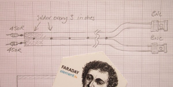
From the previous blog post, it is clear that these differential probes will offer a 1 kohm (450 + 50 + 50 + 450 ohm) resistance to the circuit under test. The connectors on the right need to be combined into a single output. To do that, a combiner/splitter type device can be used, also known as a hybrid coupler. They look like this:
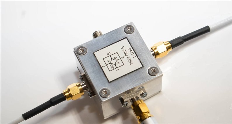
There are four connections on it. This one happens to use SMA connectors. The four connections are labelled 1, 2, S and J. The ports 1 and 2 can be used as inputs, and would be connected to the differential probes. The S port and J ports are both outputs. The S port provides the sum of the two signals with zero degrees phase shift. The J port provides the sum with 180 degrees phase shift (there are 90 degree versions too, but that is not used here).
The S port needs to be terminated in a 50 ohm load for this use-case, and the J port is attached to a spectrum analyzer (observe precautions like suitable attenuation and DC blocking if required - the low voltage tests in this blog post did not require that).
Probe Construction
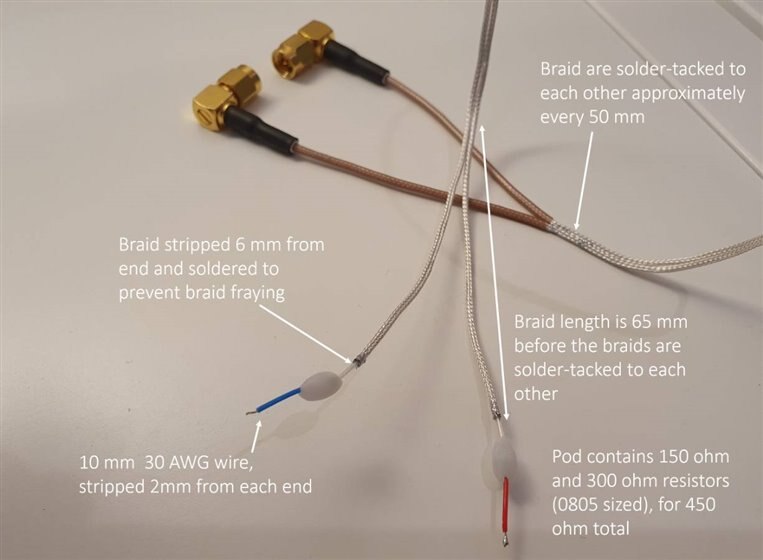
Refer to the oscilloscope probe blog post for the general idea. The overall length was about 400 mm end-to-end. The measurements in the diagram are what I used, and experimentation could yield better or worse results. Both of the coax cables should be identical length (i.e. try to match the lengths down to the millimeter), and the wire ends should be identical length too.
Connecting It Up
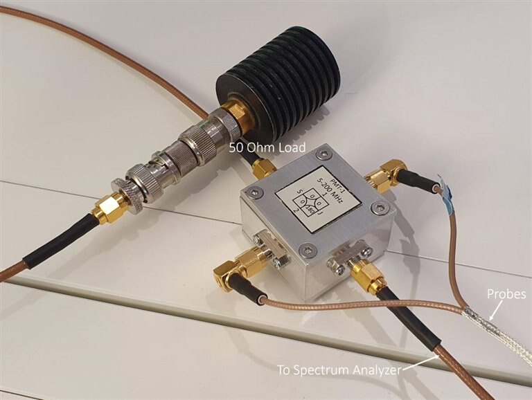
As mentioned earlier, it is good to take precautions such as inserting an attenuator and DC block if there is any risk of damaging the spectrum analyzer. The photo below shows how the connections were made. The 50 ohm load here is overkill, only a tiny screw-on load is needed. For the combiner/splitter,I used what I had which was a Minicircuits PMT-1+ device (5-200 MHz response), inserted into a metal case. The one that Jon mentioned was a ZFSCJ-2-1 device for 1-500 MHz response. I will probably purchase this one eventually: PSCJ-2-1+ for 1-200 MHz response (it's a bit lower cost).
Testing with a Bare PCB and a Signal Generator
For bare PCB testing, I took a circuit board that was intended to be an audio amplifier with input and output capacitor and an op amp circuit. The capacitors and op amp locations were all bypassed with wire. A 50 ohm resistor was placed near the end of the board (circled in yellow in the diagram below), before passing the output into the ground plane (at the green arrow location). It is a 2-layer board, and the underside is entirely a ground plane. The top side has several copper pour areas, all are ground (no power copper pour), and there are vias stitching them, all approximately spaced 8 mm apart.
The path of the signal (from the signal generator) is indicated by the yellow arrows.
The orange and blue arrows show where the input and output capacitors were intended to go, but are jumpered with bare wires. The green circled areas are ground plane where the solder mask was scraped off.
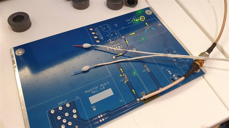
The signal generator was set to 35 MHz, -10 dBm. When I connected the differential probes across the wire links (orange or blue arrows), I saw -65 dBm on the spectrum analyzer in both cases. When I connected the probes to the green circle locations, which are ground plane (I scraped off the solder resist there), I saw -88 dBm. Of course really for a like-for-like comparison, the distance between the probes should be approximately kept similar across all measurements, I don't think it's critical at this frequency at all). And if it was a good ground plane then the distance between the probes should still result in a measurement close to the noise floor regardless of distance.
Testing with a BeagleBone Black Wireless
In order to test with a more realistic board already operational, I examined the BeagleBone Black Wireless (BBB-Wireless) circuit diagram and gerber files. The following locations were chosen for testing; they are the ends of two ceramic capacitors which drop into the ground plane. I chose these locations because as can be seen by the dashed yellow line in the gerber diagram below, the ground plane layer has a trace running through it in-between and perhaps it has a negative impact.
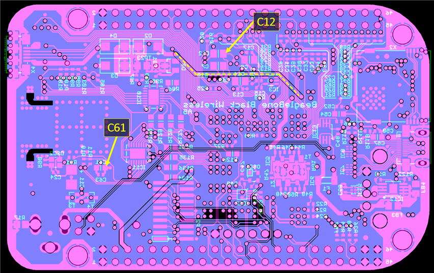
The power entry is from a 5V DC barrel socket on the BBB-Wireless, it is at the lower-left on the gerber plot shown above.
The board circuit diagram is shown below:
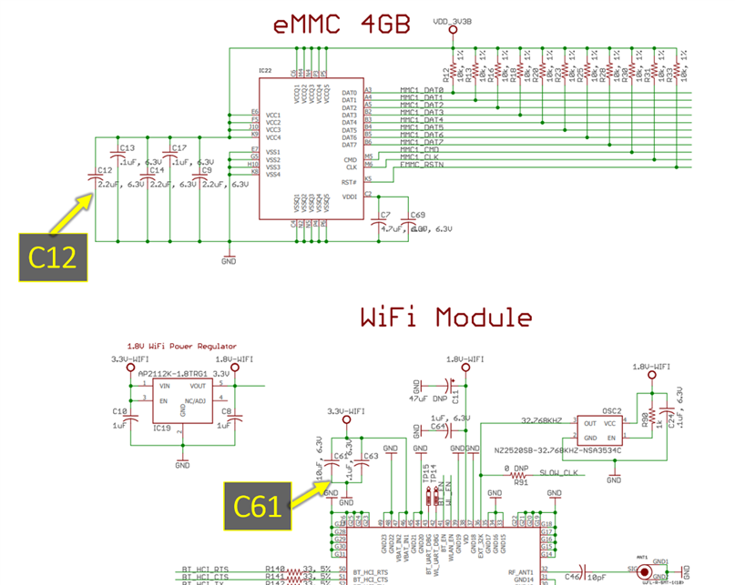
Due to the probe positions I expected to see ground plane noise whenever the eMMC memory was accessed. I did not expect to see WiFi module noise, because the power entry is more south-bound from the gerber plot.
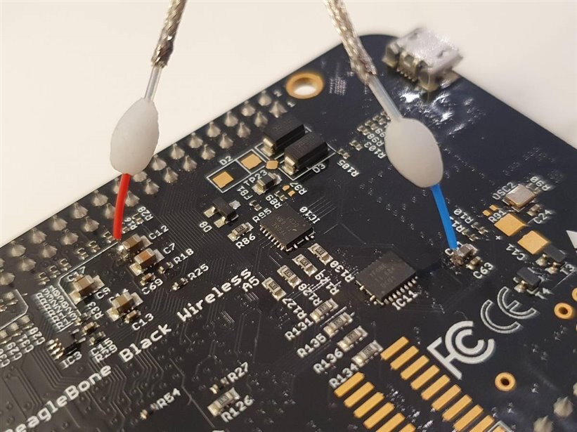
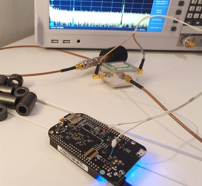
The probes were soldered into position:
The entire setup:
Network traffic was tested using iperf3 using the following commands.
Server (elsewhere, not part of the photo shown above):
iperf3 -s -f K
BBB-Wireless acting as a client (replace xx.xx.xx.xx with the IP address of the server):
iperf3 -c xx.xx.xx.xx -f -K
When the test was run, I saw no noise present on the spectrum analyzer, beyond the noise floor (depends on the spectrum analyzer settings).
This was what I was expecting anyway.
Next, to exercise the eMMC memory, the following commands were typed:
mount -t vfat /dev/mmcblk1p1 /mnt/emmc -t auto
cd /mnt/emmc
mkdir -p home/shabaz/development/disktest
cd home/shabaz/development/disktest
dd if=/dev/zero of=speedtest bs=1M count=100 conv=fdatasync
When the last command was typed, a file was written to eMMC (the eMMC chip is Kingston EMMC04G-M627-X02U). The spectrum analyzer (set up for a span of 200 MHz) showed the following:
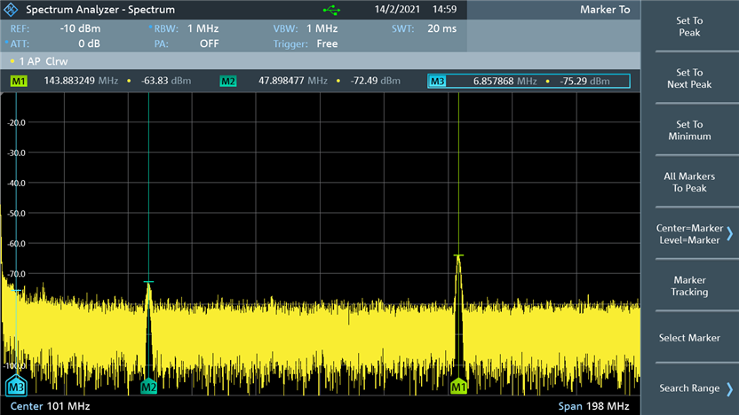
The markers M1 and M2 in the screenshot above are 148.88 MHz -63 dBm and 47.9 MHz -72 dBm respectively. Unfortunately I don't know enough about eMMC and Linux configuration to know what these signals represent!
I tried desoldering a few capacitors on the BBB-Wireless, and the noise was not impacted to any noticeable difference. Next steps could be to try to solder the probes to different locations on the BBB-Wireless. I didn't have time to try this.
Summary
With not too much effort, it is possible to assemble differential probes for measuring ground plane noise. More experimenting needs to be done, but the initial results seem promising.
I think this is a great tool for learning how currents flow in a plane, and for examining real circuits and problem-solving. It could be good to experiment further with the usability aspects of the probes too; perhaps sharp tips and insulated probe holders could be useful. genebren and jc2048 have provided some great ideas for this in the discussion comments at the previous blog post, to make use of designs that jw0752 has developed, and wooden dividers-style holders, perhaps with springy wood join.
Special thanks to Jon (jc2048 ) for helping figure the technical side of it all to get this far!
Top Comments
-

jc2048
-
Cancel
-
Vote Up
+2
Vote Down
-
-
Sign in to reply
-
More
-
Cancel
-

shabaz
in reply to jc2048
-
Cancel
-
Vote Up
+2
Vote Down
-
-
Sign in to reply
-
More
-
Cancel
Comment-

shabaz
in reply to jc2048
-
Cancel
-
Vote Up
+2
Vote Down
-
-
Sign in to reply
-
More
-
Cancel
Children