element14 Community
element14 Community
    Register Log In
  • Site
  • Search
  • Log In Register
  • About Us
  • Community Hub
    Community Hub
    • What's New on element14
    • Feedback and Support
    • Benefits of Membership
    • Personal Blogs
    • Members Area
    • Achievement Levels
  • Learn
    Learn
    • Ask an Expert
    • eBooks
    • element14 presents
    • Learning Center
    • Tech Spotlight
    • STEM Academy
    • Webinars, Training and Events
    • Learning Groups
  • Technologies
    Technologies
    • 3D Printing
    • FPGA
    • Industrial Automation
    • Internet of Things
    • Power & Energy
    • Sensors
    • Technology Groups
  • Challenges & Projects
    Challenges & Projects
    • Design Challenges
    • element14 presents Projects
    • Project14
    • Arduino Projects
    • Raspberry Pi Projects
    • Project Groups
  • Products
    Products
    • Arduino
    • Avnet Boards Community
    • Dev Tools
    • Manufacturers
    • Multicomp Pro
    • Product Groups
    • Raspberry Pi
    • RoadTests & Reviews
  • Store
    Store
    • Visit Your Store
    • Choose another store...
      • Europe
      •  Austria (German)
      •  Belgium (Dutch, French)
      •  Bulgaria (Bulgarian)
      •  Czech Republic (Czech)
      •  Denmark (Danish)
      •  Estonia (Estonian)
      •  Finland (Finnish)
      •  France (French)
      •  Germany (German)
      •  Hungary (Hungarian)
      •  Ireland
      •  Israel
      •  Italy (Italian)
      •  Latvia (Latvian)
      •  
      •  Lithuania (Lithuanian)
      •  Netherlands (Dutch)
      •  Norway (Norwegian)
      •  Poland (Polish)
      •  Portugal (Portuguese)
      •  Romania (Romanian)
      •  Russia (Russian)
      •  Slovakia (Slovak)
      •  Slovenia (Slovenian)
      •  Spain (Spanish)
      •  Sweden (Swedish)
      •  Switzerland(German, French)
      •  Turkey (Turkish)
      •  United Kingdom
      • Asia Pacific
      •  Australia
      •  China
      •  Hong Kong
      •  India
      •  Korea (Korean)
      •  Malaysia
      •  New Zealand
      •  Philippines
      •  Singapore
      •  Taiwan
      •  Thailand (Thai)
      • Americas
      •  Brazil (Portuguese)
      •  Canada
      •  Mexico (Spanish)
      •  United States
      Can't find the country/region you're looking for? Visit our export site or find a local distributor.
  • Translate
  • Profile
  • Settings
Test & Tools
  • Technologies
  • More
Test & Tools
Forum goal for 2023: use a conical solder tip and enjoy it
  • Blog
  • Forum
  • Documents
  • Files
  • Members
  • Mentions
  • Sub-Groups
  • Tags
  • More
  • Cancel
  • New
Join Test & Tools to participate - click to join for free!
Actions
  • Share
  • More
  • Cancel
Forum Thread Details
  • Replies 63 replies
  • Subscribers 354 subscribers
  • Views 25102 views
  • Users 0 members are here
Related

goal for 2023: use a conical solder tip and enjoy it

Jan Cumps
Jan Cumps over 2 years ago

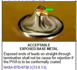
You have to challenge your habits. I have always soldered with chisel and sloped/bevel round tips.
Many irons come with a conical tip. A lot of people solder happily with it.

image

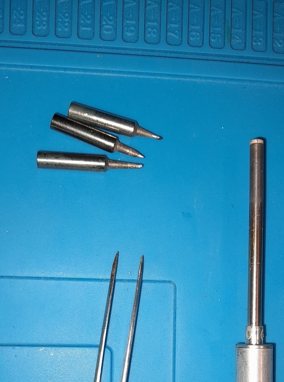
I have several, to use with an iron that I like. But I don't like soldering with the conical tips. I am not good at it.
That's going to change this year. I'm going to try and always use these tips when appropriate, and learn to love them.
The real goal is to become better at soldering with the conical versions than I am now with chisel and sloped types. And to enjoy the adaption path.

I'll keep you posted.

  • Sign in to reply
  • Cancel

Top Replies

  • shabaz
    shabaz over 2 years ago in reply to ntewinkel +5
    Hehe at least you got a choice : ) I didn't know of any other styles growing up, other than bevel. All the instructions taught everyone to use this style of tip: This is from the children's Ladybird…
  • shabaz
    shabaz over 2 years ago +4
    Maybe they are good on QFN. They look like they could be usable to drag the tip right into the corner when manually soldering QFN. I'm the same, no good with conical. Although the very finest/pointiest…
  • Gough Lui
    Gough Lui over 2 years ago +4
    I've used my conical so much that it's "turned" into a chisel :). My technique hasn't changed much really ... but I do prefer conical for the potential for fine-pitch touch-ups. Not as nice for transferring…
Parents
  • kmikemoo
    kmikemoo over 2 years ago

    I've been tempted by this thread to try a chisel tip.  Up to this point, I've only had conical.  My favorite one is the slightly offset tip (900M-T-IS).

    • Cancel
    • Vote Up +2 Vote Down
    • Sign in to reply
    • Cancel
  • Jan Cumps
    Jan Cumps over 2 years ago in reply to kmikemoo

    Seems that my post convinced more people to abandon conical than to learn it Sweat smile

    • Cancel
    • Vote Up +4 Vote Down
    • Sign in to reply
    • Cancel
  • shabaz
    shabaz over 2 years ago in reply to Jan Cumps

    It's seen a lot in videos from (say) Adafruit etc. Wrong though! (I mean if they are going to teach, they may as well try to do it properly, since it's little effort).

    • Cancel
    • Vote Up +2 Vote Down
    • Sign in to reply
    • Cancel
  • beacon_dave
    beacon_dave over 2 years ago in reply to shabaz

    Also depends if the cut is to be coated afterwards or not.

    image

    https://workmanship.nasa.gov/lib/insp/2%20books/frameset.html

    • Cancel
    • Vote Up +2 Vote Down
    • Sign in to reply
    • Cancel
  • shabaz
    shabaz over 2 years ago in reply to beacon_dave

    I think it is still cut first, i.e. this was a scenario where the soldering didn't cover the top of the joint despite it being cut beforehand. Not sure! 

    I guess this shows it must be a chemical reason, e.g. corrosion.

    • Cancel
    • Vote Up +2 Vote Down
    • Sign in to reply
    • Cancel
  • Jan Cumps
    Jan Cumps over 2 years ago in reply to shabaz

    I have an opinion®:

    the cut end of a lead is exactly the same material as all the rest of the lead. And that's exposed too.

    • Cancel
    • Vote Up +1 Vote Down
    • Sign in to reply
    • Cancel
  • beacon_dave
    beacon_dave over 2 years ago in reply to shabaz

    Yes, I was referring to the base metal sealing there.

    Strange that they let that one through though given some of the other stuff.

    I think this is the one you are after about cutting stress

    image

    • Cancel
    • Vote Up +1 Vote Down
    • Sign in to reply
    • Cancel
  • shabaz
    shabaz over 2 years ago in reply to beacon_dave

    I've not read the NASA standards, but it would be surprising if they allow component leads to be snipped on a PCB after the component is soldered. (merely from what I observed in mil-product hand assembly).  I know nothing about metallurgy/chemistry, so I'm speculating it is shock and corrosion related. But the conformal coating comment does seem to align with the corrosion theory (at the junction of the exposed copper/plating/solder perhaps, but I have no idea). 

    • Cancel
    • Vote Up +2 Vote Down
    • Sign in to reply
    • Cancel
  • hlipka
    hlipka over 2 years ago in reply to shabaz

    Here is what is done in avionics: https://www.youtube.com/watch?v=Vynb_HdEIDU . Whatever you do currently, it will not be good enough for these standards. (and yes, the cut before soldering)

    • Cancel
    • Vote Up +3 Vote Down
    • Sign in to reply
    • Cancel
  • shabaz
    shabaz over 2 years ago in reply to Jan Cumps

    You could be right, but instinctively if I see exposed copper on the end of a component, I tend to solder over it. Just habit.

    • Cancel
    • Vote Up +2 Vote Down
    • Sign in to reply
    • Cancel
  • beacon_dave
    beacon_dave over 2 years ago in reply to shabaz

    'Properly' kind of depends on which standards you are working to though.

    Also it doesn't help that some of those standards are expensive to get hold of and certification even more expensive...

    • Cancel
    • Vote Up +2 Vote Down
    • Sign in to reply
    • Cancel
  • Jan Cumps
    Jan Cumps over 2 years ago in reply to hlipka

    I saw this video series today too :). When Chris asked me to point to the Nasa videos I saw, I tried to find them back, but couldn't (maybe copyright issues?). But I found these and enjoyed watching them. There's one that takes 6 minutes to solder 1 wire into 1 connector pin <3.

    Edit:
    this one: https://youtu.be/yzkuWORme2w
    and you have to watch this one first :) : https://youtu.be/BiVkI4IooH4

    • Cancel
    • Vote Up +1 Vote Down
    • Sign in to reply
    • Cancel
Reply
  • Jan Cumps
    Jan Cumps over 2 years ago in reply to hlipka

    I saw this video series today too :). When Chris asked me to point to the Nasa videos I saw, I tried to find them back, but couldn't (maybe copyright issues?). But I found these and enjoyed watching them. There's one that takes 6 minutes to solder 1 wire into 1 connector pin <3.

    Edit:
    this one: https://youtu.be/yzkuWORme2w
    and you have to watch this one first :) : https://youtu.be/BiVkI4IooH4

    • Cancel
    • Vote Up +1 Vote Down
    • Sign in to reply
    • Cancel
Children
  • hlipka
    hlipka over 2 years ago in reply to Jan Cumps

    The video I had linked to takes about 12 minutes for one resistor. The amount of cleaning they do is kind of excessive, but the I think in avionics (or anything else where lives depend on it) you just do not take chances. This also explains why such devices are quite expensive - they just live up to a different standard that what I do at home...

    • Cancel
    • Vote Up +3 Vote Down
    • Sign in to reply
    • Cancel
  • beacon_dave
    beacon_dave over 2 years ago in reply to Jan Cumps

    It might be out of date now though... 

    "NASA has adopted IPC J-STD-001FS for all Programs and Projects, effective on October 17, 2011.  The NASA standards for soldering, NASA-STD-8739.2 and NASA-STD-8739.3, are cancelled as of October 17, 2011."

    https://nepp.nasa.gov/index.cfm/22093

    • Cancel
    • Vote Up +2 Vote Down
    • Sign in to reply
    • Cancel
  • Jan Cumps
    Jan Cumps over 2 years ago in reply to beacon_dave

    See you in an hour (of powerpoint. no soldering action)

    You don't have permission to edit metadata of this video.
    Edit media
    x
    image
    Upload Preview
    image

    • Cancel
    • Vote Up +1 Vote Down
    • Sign in to reply
    • Cancel
  • shabaz
    shabaz over 2 years ago in reply to Jan Cumps

    Slight smile

    • Cancel
    • Vote Up 0 Vote Down
    • Sign in to reply
    • Cancel
  • beacon_dave
    beacon_dave over 2 years ago in reply to Jan Cumps

    Enjoy... but haven't you skipped over NASA-STD-8739.x to IPC J-STD-001E ?

    no cheating now...  Slight smile

    • Cancel
    • Vote Up +2 Vote Down
    • Sign in to reply
    • Cancel
  • shabaz
    shabaz over 2 years ago in reply to hlipka

    I just watched the video. I'm surprised, personally I wouldn't say that my normal soldering practice is all that different, for working at a good speed. I don't think I deviate too much. I don't pre-tin, presumably it is easy for them because they have the solder bath. (I pre-tin stripped wire though, out of habit, regardless if it is solid core or stranded). I eyeball the length of the component leads instead of using that neat trick with the looped component wire, but I trim first just like they do. I form the component leads with pliers, instead of the red tool he used in the video. I certainly don't exceed 30 degrees on PCBs either, because I like the wires mostly straight, instead of combed down (I use blu-tack/putty to temporarily hold the component). (On perfboard when prototyping I will bend and use the component leads as if they were PCB tracks, but that's different). And always clean the board of flux, with this brush (it's very stiff, which works great on PCBs).

    • Cancel
    • Vote Up +2 Vote Down
    • Sign in to reply
    • Cancel
element14 Community

element14 is the first online community specifically for engineers. Connect with your peers and get expert answers to your questions.

  • Members
  • Learn
  • Technologies
  • Challenges & Projects
  • Products
  • Store
  • About Us
  • Feedback & Support
  • FAQs
  • Terms of Use
  • Privacy Policy
  • Legal and Copyright Notices
  • Sitemap
  • Cookies

An Avnet Company © 2025 Premier Farnell Limited. All Rights Reserved.

Premier Farnell Ltd, registered in England and Wales (no 00876412), registered office: Farnell House, Forge Lane, Leeds LS12 2NE.

ICP 备案号 10220084.

Follow element14

  • X
  • Facebook
  • linkedin
  • YouTube