element14 Community
element14 Community
    Register Log In
  • Site
  • Search
  • Log In Register
  • About Us
  • Community Hub
    Community Hub
    • What's New on element14
    • Feedback and Support
    • Benefits of Membership
    • Personal Blogs
    • Members Area
    • Achievement Levels
  • Learn
    Learn
    • Ask an Expert
    • eBooks
    • element14 presents
    • Learning Center
    • Tech Spotlight
    • STEM Academy
    • Webinars, Training and Events
    • Learning Groups
  • Technologies
    Technologies
    • 3D Printing
    • FPGA
    • Industrial Automation
    • Internet of Things
    • Power & Energy
    • Sensors
    • Technology Groups
  • Challenges & Projects
    Challenges & Projects
    • Design Challenges
    • element14 presents Projects
    • Project14
    • Arduino Projects
    • Raspberry Pi Projects
    • Project Groups
  • Products
    Products
    • Arduino
    • Avnet Boards Community
    • Dev Tools
    • Manufacturers
    • Multicomp Pro
    • Product Groups
    • Raspberry Pi
    • RoadTests & Reviews
  • Store
    Store
    • Visit Your Store
    • Choose another store...
      • Europe
      •  Austria (German)
      •  Belgium (Dutch, French)
      •  Bulgaria (Bulgarian)
      •  Czech Republic (Czech)
      •  Denmark (Danish)
      •  Estonia (Estonian)
      •  Finland (Finnish)
      •  France (French)
      •  Germany (German)
      •  Hungary (Hungarian)
      •  Ireland
      •  Israel
      •  Italy (Italian)
      •  Latvia (Latvian)
      •  
      •  Lithuania (Lithuanian)
      •  Netherlands (Dutch)
      •  Norway (Norwegian)
      •  Poland (Polish)
      •  Portugal (Portuguese)
      •  Romania (Romanian)
      •  Russia (Russian)
      •  Slovakia (Slovak)
      •  Slovenia (Slovenian)
      •  Spain (Spanish)
      •  Sweden (Swedish)
      •  Switzerland(German, French)
      •  Turkey (Turkish)
      •  United Kingdom
      • Asia Pacific
      •  Australia
      •  China
      •  Hong Kong
      •  India
      •  Korea (Korean)
      •  Malaysia
      •  New Zealand
      •  Philippines
      •  Singapore
      •  Taiwan
      •  Thailand (Thai)
      • Americas
      •  Brazil (Portuguese)
      •  Canada
      •  Mexico (Spanish)
      •  United States
      Can't find the country/region you're looking for? Visit our export site or find a local distributor.
  • Translate
  • Profile
  • Settings
Test & Tools
  • Technologies
  • More
Test & Tools
Documents Programmable Electronic Load - ADC and DAC BoosterPack test
  • Blog
  • Forum
  • Documents
  • Files
  • Members
  • Mentions
  • Sub-Groups
  • Tags
  • More
  • Cancel
  • New
Join Test & Tools to participate - click to join for free!
Actions
  • Share
  • More
  • Cancel
Engagement
  • Author Author: Jan Cumps
  • Date Created: 24 Nov 2017 11:12 AM Date Created
  • Last Updated Last Updated: 2 Dec 2017 10:04 AM
  • Views 4459 views
  • Likes 7 likes
  • Comments 35 comments
Related
Recommended

Programmable Electronic Load - ADC and DAC BoosterPack test

WIP


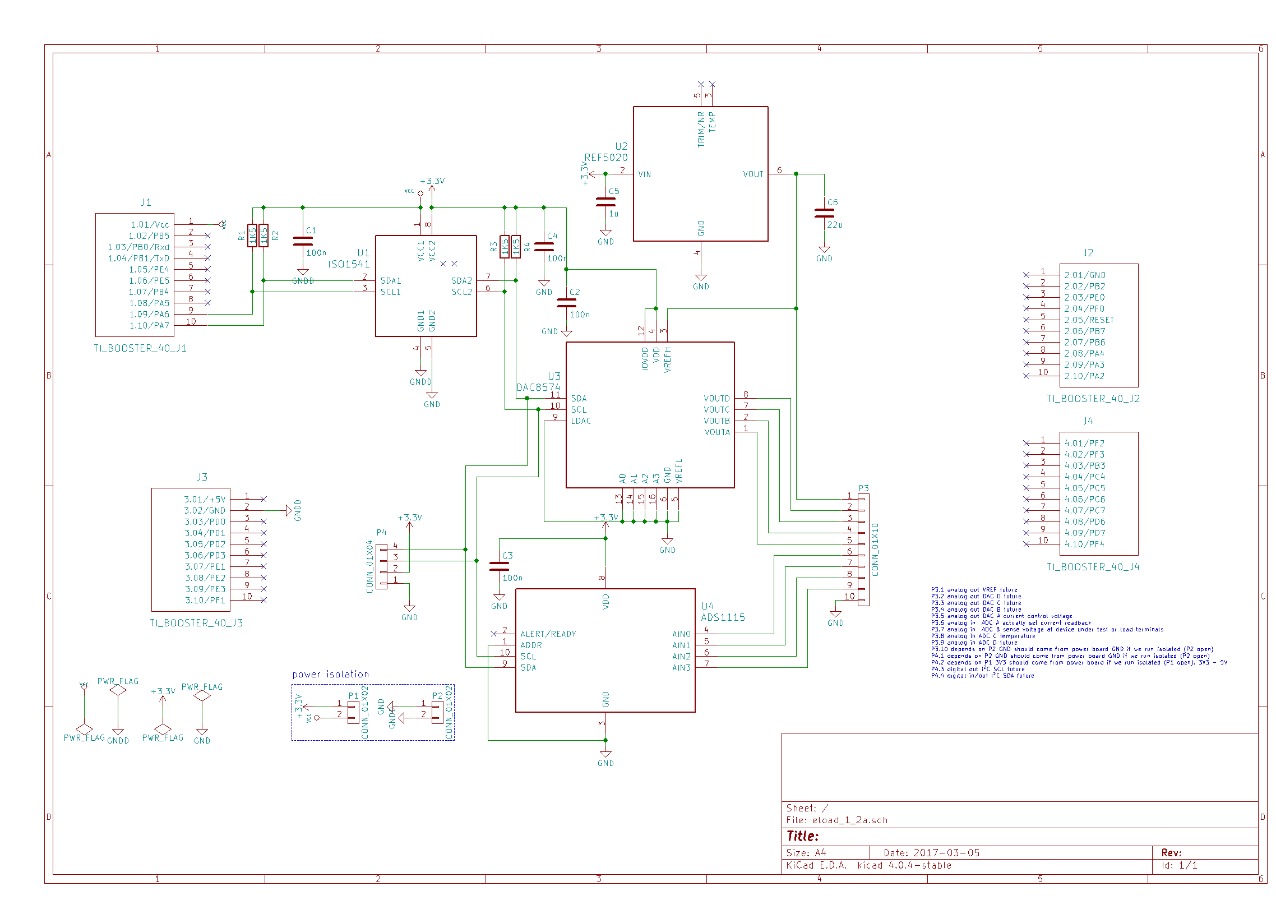
This blog documents the characteristics of the DAC/ADC BoosterPack of the electronic load that Robert Peter Oakes, jc2048 and Jan Cumps are designing.
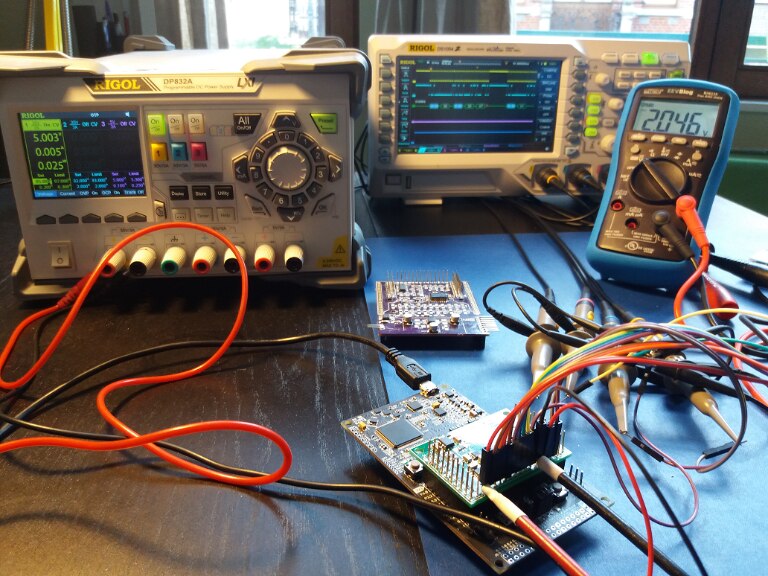
We have the same DAC/ADC BoosterPacks so we can compare the measurements of each ADC and DAC channel. Check the main document for anything related to hardware and firmware.image


Test Setup


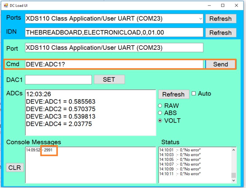
Peter has created a GUI that we can use to shoot SCPI commands. We can control the DACs and read the ADCs.

Measurements are performed with and without the power driver BoosterPack installed. We'll use 5V to power the DACs and ADCs in both situations.


image P1 and P2 on the bottom of the DAC/ADC BoosterPack have to be open. Else you'll inject 5V onto the LaunchPad 3V3 rail and you'll damage components.


It's not critical if you switch on the power supply before or after you connect the LaunchPad to your computer. The circuits are isolated.

All measurements use P3.10 as GND reference and P3.1 as reference voltage.


image


Setup without the power driver BoosterPack:

Mount the DAC/ADC BoosterPack on the LaunchPad.

Use a +5V power supply. It should be a decent one, current is approximately 5 mA.

Connect image with DAC/ADC BoosterPack P4.2  and image with P4.1.


Setup with the power driver BoosterPack:

Mount the DAC/ADC BoosterPack on the LaunchPad and the Power Driver BoosterPack on top of that.

On the Power Driver BoosterPack, bridge pins P2.4, P2.5 and P2.6 to tie both opamp inputs of opamp 3D to ground.

Use a +12V power supply. It should be a decent one, current is approximately 50 mA.

Connect image  with Power Driver BoosterPack P1.1 image  and with P1.2.


image


Measurements


In the table, the first column shows what we're measuring, the second column the SCPI command to execute with Peter's GUI.

The next columns are the measurements for Peter, Jon or Jan with and without the Power Driver BoosterPack.

The last column is for comments. We can indicate odds, errors, learnings.


JonPeterJan
Data PointSCPIWithoutWithWithoutWithWithoutWithMeasurement method
SupplyN/A4.989 V11.88 VDMM
DAC/ADC V+N/A4.989 V5.035 VDMM
VREFN/A2.046 V2.046 VDMM
ADC A GNDDEVE:ADC1?2SCPI output
ADC A VREFDEVE:ADC1?10918SCPI output
ADC ADEVE:ADC1?1138SCPI output
ADC B GNDDEVE:ADC2?12SCPI output
ADC B VREFDEVE:ADC2?10920SCPI output
ADC BDEVE:ADC2?1
SCPI output
ADC C GNDDEVE:ADC3?22SCPI output
ADC C VREFDEVE:ADC3?1092010919SCPI output
ADC CDEVE:ADC3?26868SCPI output
ADC D GNDDEVE:ADC4?83SCPI output
ADC D VREFDEVE:ADC4?1091910919SCPI output
DAC A 0DEVE:DAC1 00.000 V0.001 VDMM
DAC A maxDEVE:DAC1 655352.040 V2.040 VDMM
DAC B 0DEVE:DAC2 00.005 V0.005 VDMM
DAC B maxDEVE:DAC2 655352.046 V2.046 VDMM
DAC C 0DEVE:DAC3 00.000 V0.000 VDMM
DAC C maxDEVE:DAC3 655352.039 V V2.039 VDMM
DAC D 0DEVE:DAC4 00.000 V0.000 VDMM
DAC D maxDEVE:DAC4 655352.039 V2.039 VDMM


To resolve

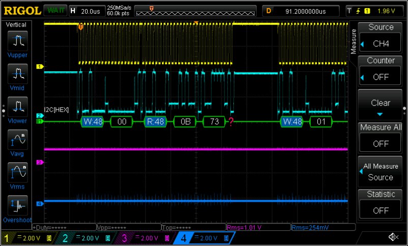
With the power driver installed, ADC C and D act strange (probably also A and B, but I didn't inject a voltage in them because they are connected to opamp pins).

In particular strange for ADC D, because that one isn't routed. Strange.

I will try to decrease the frequency of the sample speed and the i²c speed to see if it's related to that ...


Follow up: the cause is that OPAMP 3C injects -0.8V into ADC A. All measurements are off when that happens. As soon as I force ADC A positive (by tying it to ground or a positive voltage) all measurements are correct.


image


We have a separate document to analyse the summing node at zero.

  • metrology
  • boosterpack
  • msp432
  • ti-rtos
  • launchpad
  • laboratory
  • instrument
  • Share
  • History
  • More
  • Cancel
  • Sign in to reply

Top Comments

  • shabaz
    shabaz over 7 years ago +3
    Hi Jan, I was wondering, what are the expected values, is it reading a value representing 1.602V when it should read a value representing 2.048V? I'm wondering if it could be due to conversion time (i…
  • Jan Cumps
    Jan Cumps over 7 years ago in reply to shabaz +3
    yes, Shabaz, I have a controlled value of 2.040 V. Once I mount my additional driver board (self-designed so many things can be wrong ) the ADC says it’s 1.6 V. I checked signals with my scope to see if…
  • jc2048
    jc2048 over 5 years ago in reply to Andrew J +3
    Andrew J , have you read the blog I did when building Jan and Peter's load? That has some material on the low end of the DAC. Long story short, I adapted the analogue stuff after the DAC so the output…
Parents
  • shabaz
    shabaz over 7 years ago

    Hi Jan,


    I was wondering, what are the expected values, is it reading a value representing 1.602V when it should read a value representing 2.048V?

    I'm wondering if it could be due to conversion time (i.e. once the ADC has been requested to perform the conversion, the delay until the conversion result is read may be too short in the code currently). Could that be likely, or is the delay quite long for the tests you did?

    • Cancel
    • Vote Up +3 Vote Down
    • Sign in to reply
    • More
    • Cancel
  • Jan Cumps
    Jan Cumps over 7 years ago in reply to shabaz

    yes, Shabaz, I have a controlled value of 2.040 V. Once I mount my additional driver board (self-designed so many things can be wrong image ) the ADC says it’s 1.6 V. I checked signals with my scope to see if there isn’t noise or oscillation.


    I will give each of the 4 ADC units a little more time to see if this resolves my issue ...

    • Cancel
    • Vote Up +3 Vote Down
    • Sign in to reply
    • More
    • Cancel
Comment
  • Jan Cumps
    Jan Cumps over 7 years ago in reply to shabaz

    yes, Shabaz, I have a controlled value of 2.040 V. Once I mount my additional driver board (self-designed so many things can be wrong image ) the ADC says it’s 1.6 V. I checked signals with my scope to see if there isn’t noise or oscillation.


    I will give each of the 4 ADC units a little more time to see if this resolves my issue ...

    • Cancel
    • Vote Up +3 Vote Down
    • Sign in to reply
    • More
    • Cancel
Children
  • Jan Cumps
    Jan Cumps over 7 years ago in reply to Jan Cumps

    there’s also an additional i2c device on that driver board that I haven’t programmed yet. that could also be a source of issues. it’s sharing the lines with the ADC and DAC ic.

    • Cancel
    • Vote Up +2 Vote Down
    • Sign in to reply
    • More
    • Cancel
element14 Community

element14 is the first online community specifically for engineers. Connect with your peers and get expert answers to your questions.

  • Members
  • Learn
  • Technologies
  • Challenges & Projects
  • Products
  • Store
  • About Us
  • Feedback & Support
  • FAQs
  • Terms of Use
  • Privacy Policy
  • Legal and Copyright Notices
  • Sitemap
  • Cookies

An Avnet Company © 2025 Premier Farnell Limited. All Rights Reserved.

Premier Farnell Ltd, registered in England and Wales (no 00876412), registered office: Farnell House, Forge Lane, Leeds LS12 2NE.

ICP 备案号 10220084.

Follow element14

  • X
  • Facebook
  • linkedin
  • YouTube