Hello everyone.
In this eleventh blog post I will show my third experiment which I promised in my first blog post as part of Experimenting with Current Sense Amplifiers Design Challenge. In blogs #2, #3 and #4 I shown basic usage of MAX40080 Current Sense Amplifier sensor. Then in blog posts #5, #6 and #7 I introduced my libraries which I created as part contest for simplifying usage of MAX40080 CSA sensor. In blog post #8 I introduced my CLI utility for allowing use MAX40080 CSA without need of programming. In blog #9 and #10 I shown my experiments ending with analysis self-collected power consumption of Raspberry Pi. This blog post describes my main project as part of this competition.
In this blog post I upgrade setup for measuring power consumption of USB devices to support USB Type-C device (iPhone) and measure its power consumption when charging. In this project I replace Raspberry Pi by microcontroller. From current sensing point of view, project will be almost the same as previous – I will sense current flowing through USB (now Type-C) cable.
Sample Sponsors
Project shown in this blog post was supported by company Adam Tech by sending free samples of high-quality USB Type-C Receptacle USB-C31-S-RA-CS1D-BK-T/R. This part has slightly extended SMD pads, so it is possible to solder it in hand (which I successfully did). If you are interested in designing with this connector, you can download Kicad symbol and footprint library at the end of this page as part of Kicad project ZIP file.

Overview
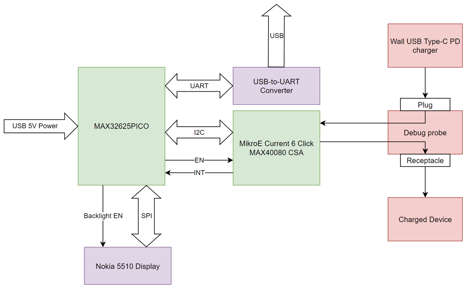
My project which I did as part of this contest is based on MAX32625 microcontroller. MAX32625 is very tiny, so I use MAX32625PICO board for using them. Current 6 Click Board is connected to this MCU including enable and interrupt wires. Outputs are shown on display usually referred by hobbyist as Nokia 5510. Current 6 Click Board is connected to the debug probe which I will show later. Debug probe has 2 USB Type-C connectors. One receptacle and one plug. All signals except power wire are directly connected from plug to receptacle. Power wire is connected to the terminal socket for connecting CSA sensor to the circuit.
Block diagram
Block diagram of project looks as follows:
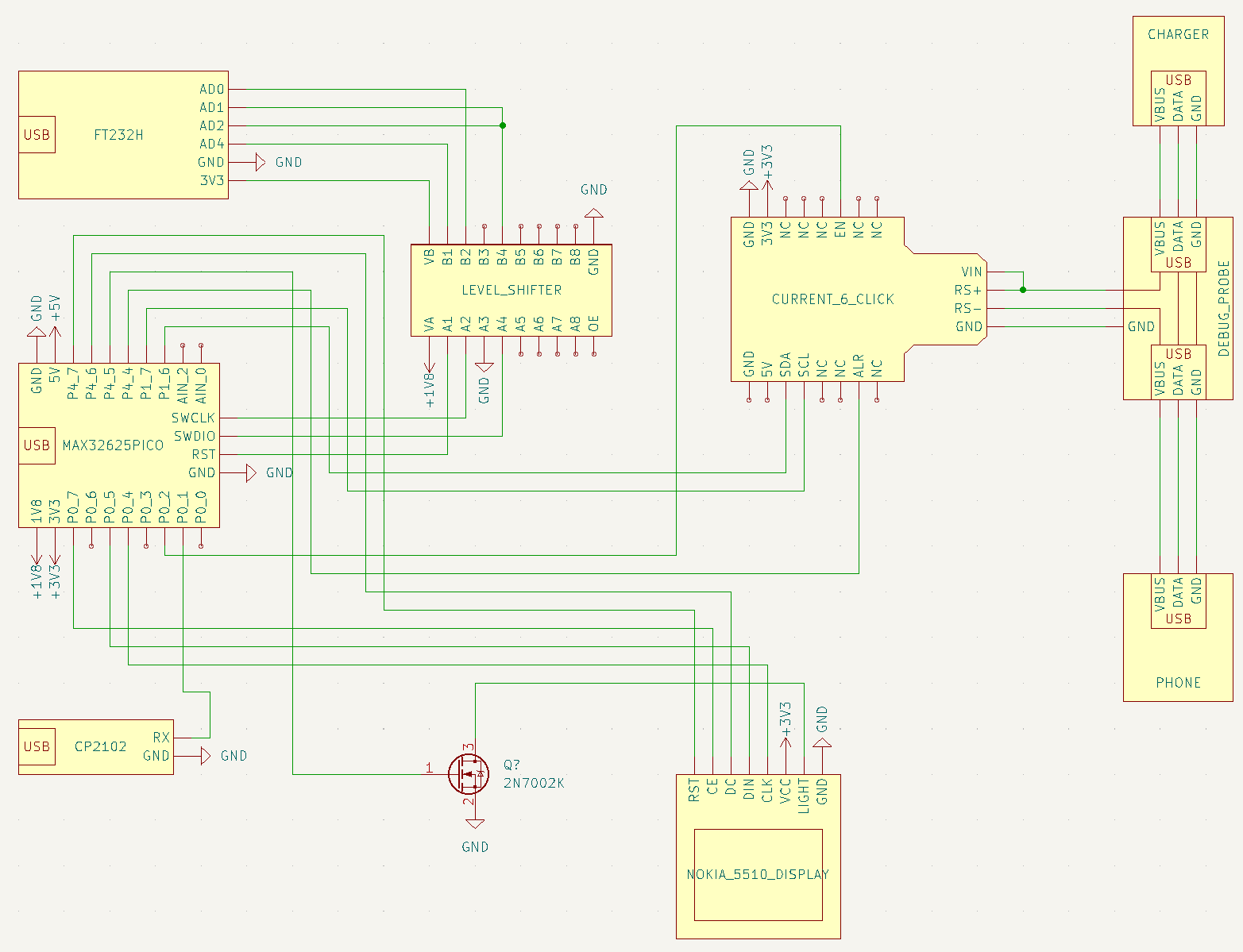
Full schematic of setup is slightly more complicated, and I also included SWD/JTAG debugger (FT232H) and required level shifter. USB to UART converter is CP2102.
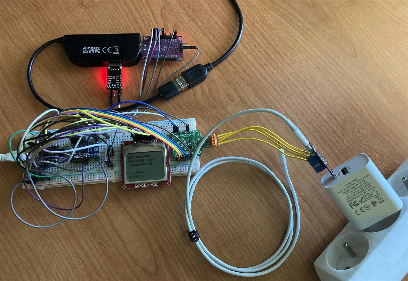
This circuit I connected on breadboard. As you can see it is lot of wires.
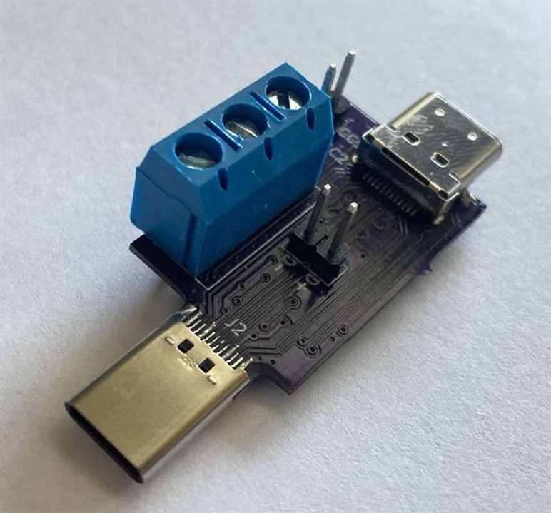
Debugging probe
For sensing current inside USB Type-C cable I used PCB which I designed. It is similar debug probe which I used in previous experiments described in blogs #9 and #10 but targets USB Type-C Rather than old legacy USB connectors.
Because USB Type-C connectors has lot of wires, schematics is more complicated than it was in previous case:
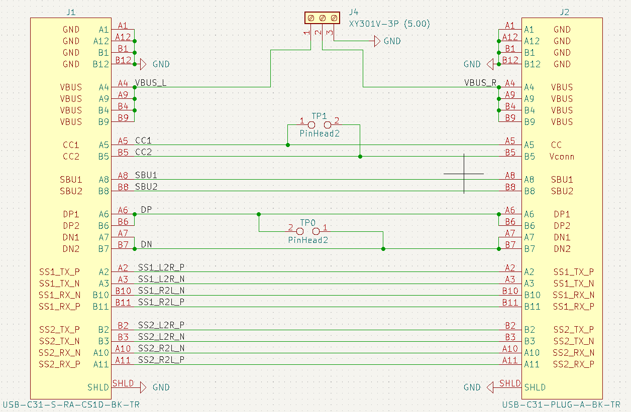
After placing components to the PCB:

Firmware
I wrote firmware for MAX32625 MCU utilizing setup described above. At development time instead of using debug probe, charger, and phone I used simpler setup with static power consumption caused by resistor.
Firmware is written in C and is based on my library which I shown in 6th blog post. I developed firmware in Eclipse IDE provided by Maxim Integrated as part of Low Power ARM Micro SDK (Win).
Firmware configures MAX40080 CSA over I2C bus and can power cycle sensor by toggling EN pin. Firmware uses interrupt from sensor. In this experiment I used sensor differently than in previous case. I configured feature called FIFO Overflow warning, which triggers interrupt when FIFO utilization reaches configured threshold (5 available samples in my case). After this happens, I collect all 5 samples at once (in fact, it is done using 5 transactions because MAX40080 does not support burst due to sending CRC byte, but transactions are executed without any delay between).
Parameters of MAX40080 configuration are following:
- Input Range is set to 50 mV for allowing sensing currents up to 5A instead of default 1A
- Operation mode of sensor is active
- Sensor store both current and voltage to the FIFO
- ADC sample rate is limited to 0.5 ksps because I am sampling both variables
- Packet Error Checking is enabled and library checks for CRC errors.
- Digital filter is set to 8 for reducing refresh rate when displaying measured values on display
- FIFO Overflow Warning and FIFO overflown are interrupts which cause INT line to assert. Other interrupts set flag in register but they do not cause INT line to fire interrupt.
- FIFO Overflow warning level is set to 5 as mentioned above.
On the display I show actual current and voltage and based on this data I show information that some device is or is not connected. This I determine based on measured current. If current is less than 10 mA (no matter of direction) then I consider this as a noise and no device is connected (or it is connected but do not consume any current). Finally I compute total consumed energy as multiplication of voltage, current and “soft-integral“ by period of time when this sample were valid.
Last feature which I added to design is capability of driving backlight of display. When no device is connected, then I turn display backlight off. I am using NMOS transistor for switching backlight.
Testing with real device
After I developed the device I unconnected testing circuit creating static power consumption by resistor and connected debug probe instead. After I connected charger (but not the phone yet) to test probe, something strange happened. My program started reporting errors on I2C bus. Sometimes it crashed with PEC error meaning that some bit error occurred while transmitting data, sometime more serious I2C errors like missing ACK and timeouts start occurring. But generally, after short period of time situation stabilized and I was sensing voltage from the power charger. But more serious behaviour happened when I also connected phone to the circuit. It starts charging but I2C communication stopped working at all. Sensor ACKed very few of requests and there were bit errors even on ACKed packets. I have no oscilloscope so I can’t see what happened with the signal on the bus, but I used logic analyser, and everything looked OK, except packets were not ACKed. After disconnecting phone from charger my program usually stuck at some software infinite loop or I2C drivers of MAX32625 or MAX40080 stuck in some deadlock state holding data line low. When investigating this issue, I noticed that simple touching and moving wires on my breadboard can make reduce this effect or make it even worse. But impact of this was not significant and even after many attemps I did not resolved it by just rearranging wires. I also tried with powering debug probe by USB Type-C port of my notebook and issue did not occured (but port is not PD capable, so it is quite useless for my experiment). I think the issue is caused by some noise coming from the charger by interconnecting grounds of charger and my circuits but cannot prove/verify/test this thought.
In this moment I realized that making these complicated projects on breadboard is not a good idea. Consequently, I implemented following techniques to try mitigating the issue:
- I implemented better error handling and reporting mechanism and removed simple infinite loop error handlers from my code.
- I implemented techniques to recover from fault state. When some hard I2C error occur, I power cycle the sensor by EN pin, restart I2C driver at MAX32625 side and reconfigure sensor again.
- I noticed that there is “significant” voltage drop about 0.15V on between GNDs of components. This is caused by non-ideal wires and it is the same issue which I faced and described in previous experiment described in blog #10. So, I used better wire for connecting grounds between parts of circuit.
- Instead of using two wire cable for connecting I2C I used four wire cable. Middle two wires I used as SDA and SCL and border two wires I connected to ground for making this cable more immune to inference with other wires on the breadboard.
After I applied these strategies, problem has significantly reduced, and I was able to collect some readings when both charger and phone was connected to the circuit, but some significant noises were still here. Unluckily I do not own oscilloscope for better analysis what is happening there. Maybe some simple filter or just capacitor can resolve this issue, but my analog knowledge is very low in this area.
Excluding this issue, I was able to see what I originally wanted to see and that’s why I did this experiment. After connecting iPhone to charger, charging started with voltage set to standard 5V used on VBUS of USB. But after short period of time (few seconds) iPhone started negotiating increasing voltage and charger accepted this and increased voltage from 5V to 9V. After switching to 9V my circuit started to be more unstable as I mentioned above and measurements were on the display interleaved with error messages, but 9V can be seen here so it is nice. In between switching voltage It looks that charger for short period of time disabled power output because my sensor noticed current near zero and MCU disabled display backlight. But after this short disconnection, 9V appeared on the VBUS and sensor started sensing it. You can see this experiment the following video:
Summary
I consider this project/experiment as partially failed. While it satisfied my expectations, and I was able to see that PD negotiation really happened and voltage changed, many I2C errors make this less usable practically. I do not recommend trying this on breadboard. I faced to lot of issues and I spend hours with debugging it. I also recommend using better wires then cheap Chinese dupont wires which are for example bundled with many non-official Arduino starter kits. They are (cheap and) good for basic tasks, but issues can arise very soon as I have seen.
Resources
At following links, you can download all resources which I created when implementing this project:
- Project schematics (PDF)
- Debug probe schematics (PDF)
- Debug probe gerbers (ZIP)
- Debug probe Kicad project (ZIP)
- Debug probe OSHPark direct link (3pcs of PCB cost $4.25 as of 2022-06-05. PCB must be 0.8mm thick and 2oz of copper should be included. Standard 1.6mm PCB wont fit into USB Type-C Plug connector)
- Firmware source code (ZIP)
- Firmware binary (ELF)
This is all from my main experiment as part of Experimenting with Current Sense Amplifiers Design Challenge. Thank you for reading this blog post. I welcome any feedback, so feel free to comment below. In next blog post I will show my last experiment. Then I most probably will write some blog post about one issue which I was discussing with Maxim support and finally, I will post summary blog post as part of this competition. Deadline is in one/two days (depending on time zone), so I will be very busy these two days. Thank you for reading it again, stay tuned for my last blogs and have a nice day.

