Introduction
In my previous blog for the Eye On Intelligence Design Challenge, I used the Zynq analog-to-digital converter (XADC) to sample the analog signal from a Wheatstone bridge load cell, amplified with an AD8226 instrumentation amplifier. The sampled data was read from a Jupyter notebook on a PYNQ distribution running on Ubuntu, using the dual-core ARM Cortex-A9 processor. The results were very promising and sufficient for my smart scale project.
Some community members suggested that a more appropriate and cost-effective solution would be to use an analog-to-digital converter specifically designed for measurements with Wheatstone bridges. Michael Kellet mentioned that TI and Analog Devices both offer ADCs designed for this purpose, which perform better than the Zynq because they can use the load cell’s excitation voltage as the reference voltage for the ADC. The TI ADS1230, for example, is a suitable low-cost ADC for this kind of application. It costs about the same as the AD8226 but includes the amplifier, ADC, and excitation referencing all in one chip.
In this new blog, I explore this path using a specialized analog-to-digital converter and designing a hardware driver that implements a simplified SPI protocol

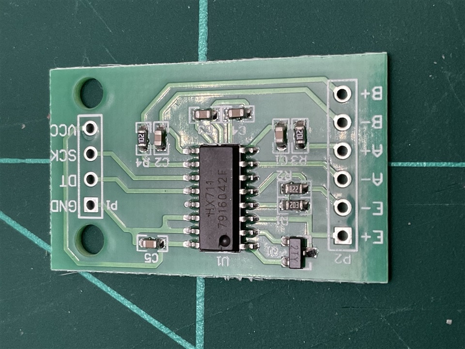
HX711: A Precision 24-Bit ADC for Weigh Scales
During the research phase for this project, I acquired a DIY scale kit that contains a similar ADC chip, the HX711. In this blog, I will explain how I managed to communicate with it from the Zynq and integrate it into the project. While this may not be the most optimal approach, it allows us to explore developing a specialized hardware accelerator for a serial protocol using the FPGA fabric, thereby freeing the system from that task. We will create a basic version of an SPI protocol, focusing on the MISO (Master Input Slave Output) communication.
The HX711 is advertised as a high-precision 24-bit Analog-to-Digital Converter (ADC) specifically designed for weigh scale and industrial control applications. This ADC offers a solution for interfacing directly with bridge sensors, simplifying the design process. HX711 Datasheet: https://cdn.sparkfun.com/assets/b/f/5/a/e/hx711F_EN.pdf
Key features of the HX711 include:
- Dual Input Channels: The HX711 can accommodate two differential input channels (A and B).
- Programmable Gain Amplifier (PGA): The on-chip PGA provides selectable gains of 32, 64, and 128, enabling precise amplification of input signals.
- On-Chip Power Supply Regulator: The integrated power supply regulator eliminates the need for external power supply components, simplifying the design.
- Flexible Clock Input: The HX711 supports both external clock sources and an internal oscillator, providing flexibility in clocking options.
- Simple Digital Interface: The device uses a simple pin-driven control interface, requiring no programming.
- Low Power Consumption: The HX711 consumes minimal power, making it suitable for battery-powered applications.
Serial Communication Protocol for HX711
The HX711 employs a simple serial communication protocol to control its operation and retrieve measurement data.
The primary pins involved are:
- PD_SCK: Serial clock input
- DOUT: Serial data output
Data Retrieval Process
The following timing diagram illustrates the data output, input, and gain selection timing and control for the serial communication.
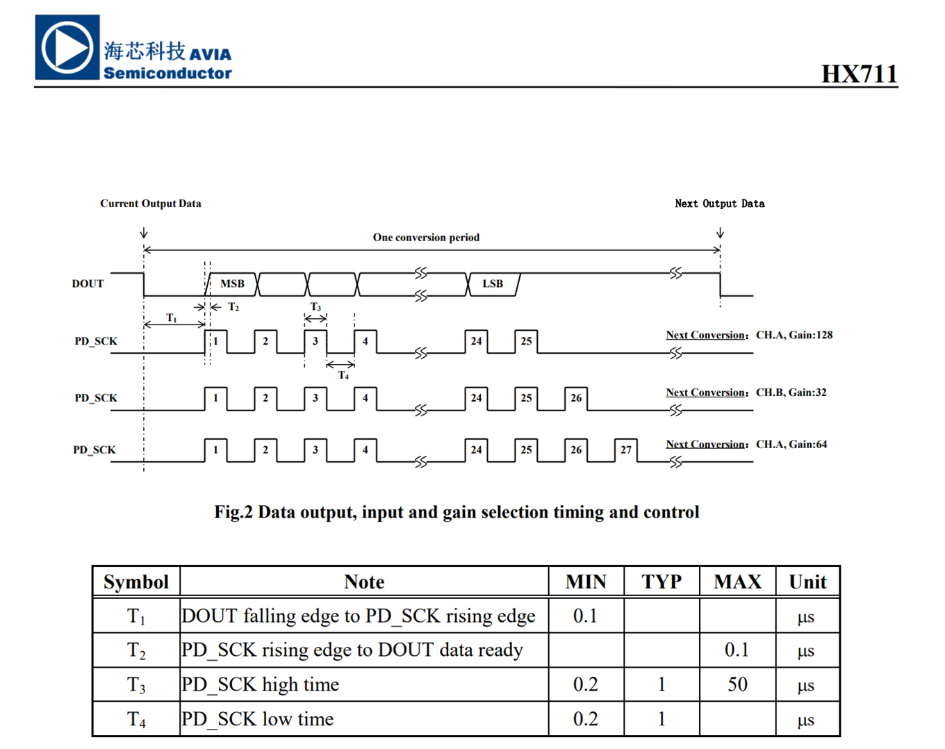
- Idle State: the HX711 is not actively transmitting data.
- DOUT is high, indicating that no data is ready.
- PD_SCK should be low.
- Data Ready:
- DOUT goes low, signaling that 24 bits of data are ready for retrieval.
- Clocking Data Out:
- Apply 25-27 positive clock pulses to PD_SCK.
- Each pulse shifts out one bit of data, starting with the most significant bit (MSB).
- After 24 bits, the 25th pulse pulls DOUT high, returning to the idle state.
- Input Channel and Gain Selection
- The number of clock pulses applied to PD_SCK determines the input channel and gain.
Hardware Implementation of an HX711 Driver in HDL (SystemVerilog) using FPGA
The HX711 driver requires precise timing and control to communicate with the sensor and extract accurate weight data. A Finite State Machine with Datapath (FSMD) is an ideal approach to implement this logic in hardware using a Hardware Description Language (HDL) like SystemVerilog.
FSMDs extend traditional Finite State Machines (FSMs) by incorporating storage elements and signal declarations. This enables more complex data processing and control within the state machine, making them well-suited for the HX711 driver.
In this implementation, the FSMD will control the timing of the clock signal, the sampling of data bits, and the selection of the gain setting. By carefully sequencing these operations, we can accurately acquire weight data from the HX711.
FSM States and Transitions:
The FSM for the HX711 driver will include the following states:
- Idle: The initial state where the driver is waiting for a start signal.
- Data Ready: The state where the driver detects that the HX711 has new data ready.
- Clocking Data: The state where the driver sends clock pulses to the HX711 to read the 24-bit data.
- Gain Selection: The state where the driver selects the desired gain setting for the HX711.
- Done: The final state where the driver has finished reading the data and is ready for the next measurement.
We will merge the idle state with the done state.
FSM Transitions:
The FSM transitions between these states based on the following conditions:
- Start Signal: A start signal initiates the data acquisition process.
- Data Ready Signal: A signal from the HX711 indicating that new data is available.
- Clock Pulse Counter: A counter that tracks the number of clock pulses sent to the HX711.
- Gain Selection Signal: A signal to select the desired gain setting.
The provided ASM chart visually represents the finite state machine (FSM) that controls the HX711 driver.
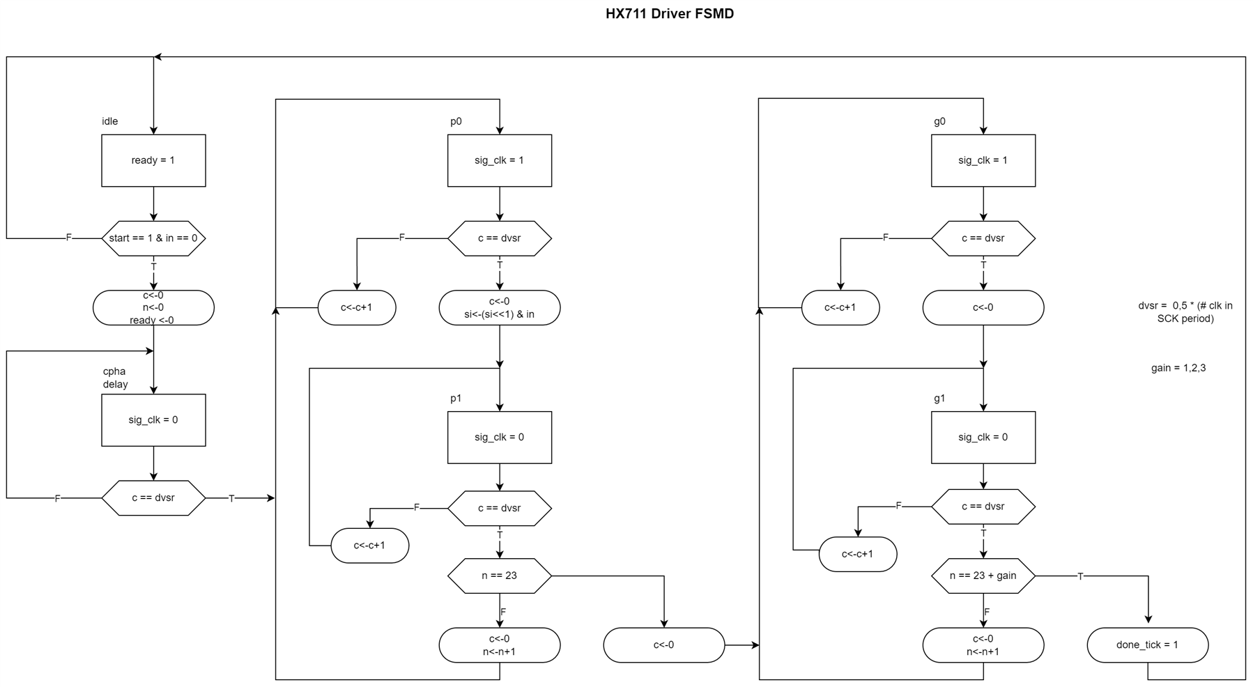
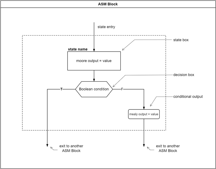
An ASM chart is a graphical representation of a digital system's behavior. It's used in digital design to visualize the sequential logic of a system.
Key Components of an ASM Chart:
- State Box: Represents a specific state of the system.
- Decision Box: Determines the next state based on a condition.
- Conditional Output Box: Generates outputs based on specific conditions.
Introduction to the HX711 Driver HDL Implementation
While I previously studied VHDL in university, I've found SystemVerilog to be a more intuitive hardware description language for digital design. Therefore, I've chosen to implement this driver using SystemVerilog.
This SystemVerilog module implements a driver for the HX711 24-bit analog-to-digital converter (ADC).
`timescale 1ns / 1ps
//////////////////////////////////////////////////////////////////////////////////

// Create Date: 10/20/2024 11:35:12 AM
// Author: Enrique Albertos (javagoza)
// Design Name: Driver for the hx711 24-Bit Analog-to-Digital Converter (ADC) for Weigh Scales
// Module Name: hx711driver_test
// Project Name: FruitVision Scale
// Target Devices: Zynq 7020
// Tool Versions: Vivado 2022.1, 2022.2
// Description: Driver
//
// Dependencies:
//
// Revision:
// Revision 0.01 - File Created
// Additional Comments:
//
//////////////////////////////////////////////////////////////////////////////////
module hx711driver (
    input clk,
    input reset,
    input logic [15:0] dvsr, // 0,5 * (# clk in SCK period)
    input logic start,
    output logic [23:0] dout,
    output logic hx711_done_tick,
    output logic ready,
    output logic sclk,
    input logic hx711_in
);

// FSM state type
typedef enum {idle, cpha_delay, p0, p1, g0, g1} state_type;

// p0, p1 hx711 signal clock half periods data in
// g0, g1 hx711 signal clock half periods gain selection
// cpha_delay to sample on the second edge

// State register
state_type state_reg;
state_type state_next;

// Clock signal generation
logic p_clk;

// Clock divider counter
logic [15:0] c_reg;
logic [15:0] c_next;

// HX711 clock signal
logic hx711_clk_reg;
logic hx711_clk_next;

// Ready signal
logic ready_i;

// Done tick signal
logic hx711_done_tick_i;

// Bit counter
logic [5:0] n_reg;
logic [5:0] n_next;

// Data input register
logic [23:0] si_reg;
logic [23:0] si_next;


// body fsm for receiving 24 bits  register
always_ff @(posedge clk, posedge reset)
    if (reset) begin
        state_reg <= idle;
        si_reg <= 0;
        n_reg <= 0;
        c_reg <= 0;
        hx711_clk_reg <= 0;
    end
    else begin
        state_reg <= state_next;
        si_reg <= si_next;
        n_reg <= n_next;
        c_reg <= c_next;
        hx711_clk_reg <= hx711_clk_next;
    end

// FSM next state logic
always_comb
begin
    state_next = state_reg; // Default state: the same
    ready_i = 0;
    hx711_done_tick_i = 0;
    si_next = si_reg;
    n_next = n_reg;
    c_next = c_reg;
    case (state_reg)
        idle: begin
                ready_i = 1; // Indicate that the data is ready
                if (start & !hx711_in) begin // Start signal and HX711 input is low
                    n_next = 0; // Reset bit counter
                    c_next =0;  // Reset clock divider counter
                    state_next = cpha_delay; // Transition to delay state
                end
            end
        cpha_delay: begin
                if (c_reg==dvsr) begin // Delay period reached
                    state_next = p0; // Transition to first clock phase
                    c_next = 0;  // Reset clock divider counter
                end
                else
                    c_next = c_reg + 1; // Increment clock divider counter
            end
        p0: begin
                if (c_reg==dvsr) begin // First clock phase completed
                    state_next = p1;  // Transition to second clock phase
                    si_next = {si_reg[22:0], hx711_in}; // Shift in new bit
                    c_next = 0; // Reset clock divider counter
                end
                else
                    c_next = c_reg + 1;  // Increment clock divider counter
            end
        p1: begin
                if (c_reg==dvsr) begin // Second clock phase completed
                    if (n_reg==23) begin // All 24 bits read
                        state_next = g0; // Transition to gain selection phase
                        c_next = 0; // Reset clock divider counter
                    end
                    else begin
                        state_next = p0;  // Transition to next bit
                        n_next = n_reg + 1;  // Increment bit counter
                        c_next = 0;  // Reset clock divider counter
                    end
                end
                else
                    c_next = c_reg + 1; // Increment clock divider counter
            end
        g0: begin
                if (c_reg==dvsr) begin // First gain selection phase completed
                    state_next = g1; // Transition to second gain selection phase
                    c_next = 0; // Reset clock divider counter
                end
                else
                    c_next = c_reg + 1;  // Increment clock divider counter
            end
        g1: begin
                if (c_reg==dvsr) begin // Second gain selection phase completed
                    hx711_done_tick_i = 1;  // Indicate data acquisition is complete
                    state_next = idle;  // Transition to idle state
                end
                else
                    c_next = c_reg + 1; // Increment clock divider counter
            end
     endcase
end

// Assign output signals
assign ready = ready_i;
assign hx711_done_tick = hx711_done_tick_i;

// Clock signal generation
assign p_clk = (state_next==p0) || (state_next == g0);
assign hx711_clk_next = p_clk;

// Output assignment
assign dout = si_reg;
assign sclk = hx711_clk_reg;


endmodule
Key Components and Functionality of my implementation. My implementation follows a design similar to most SPI circuit designs, but it only handles the master-out slave-in communication. It's a customized design to save FPGA resources.
Finite State Machine (FSM):
- The core of the driver is a state machine that controls the timing and sequence of operations for reading data from the HX711.
- The FSM transitions through the following states:
- idle: The initial state, waiting for a start signal.
- cpha_delay: A delay state to ensure proper sampling on the second clock edge.
- p0 and p1: States for the first half-period of the clock cycle, where data is sampled from the HX711.
- g0 and g1: States for the second half-period of the clock cycle, where the gain selection bits are sent to the HX711.
- done: The final state, indicating that the 24-bit data has been read.
- Timing Control:
- The dvsr input parameter controls the clock period, allowing for flexible timing adjustments.
- A counter (c_reg) is used to accurately time the clock pulses and data capture.
- Data Capture:
- The si_reg register stores the 24-bit data read from the HX711.
- The n_reg counter keeps track of the number of bits read.
- Output Signals:
- dout: Outputs the 24-bit data.
- hx711_done_tick: Indicates when a complete data acquisition cycle is finished.
- ready: Indicates whether the driver is ready to start a new measurement.
- sclk: The clock signal sent to the HX711.
Overall Operation:
- The driver waits in the idle state until a start signal is received.
- It transitions to the cpha_delay state to align with the HX711's clock phase.
- In the p0 and p1 states, the driver samples the data from the HX711 and shifts it into the si_reg register.
- In the g0 and g1 states, the driver sends the gain selection bits to the HX711.
- Once all 24 bits are read, the driver transitions to the done state and sets the hx711_done_tick signal.
Using a test bench to test our HX711 driver module
To verify the module's design, we'll create a testbench, a type of unit test. A test bench is HDL (Hardware Description Language) code designed for simulation purposes. It serves to:
- Instantiate and initialize the design.
- Generate and apply stimuli to the design.
- Monitor the design output and optionally check for functional correctness.
Additionally, a test bench can be configured to display the simulation output as a file, a waveform, or on a display screen. Its structure can be simple, applying stimuli sequentially to specific inputs.
First, we create our testbench to instantiate our HX711 driver module. Then, we assign default values for the test conditions. After that, we simulate the behaviors of the HX711 from when the signal indicates it is busy to when it has data ready. We also simulate the transmission of several values. In this test, we first simulate the transmission of the value 0xFFFFFF, followed by the value 0x000000.
`timescale 1ns / 1ps

module hx711driver_test(

    );

 // input signals
 logic clk;
 logic reset;
 logic [15:0] dvsr; // 0,5 * (# clk in SCK period)
 logic start;


 // output signals
 logic hx711_done_tick;
 logic ready;

 logic hx711_in;
 logic sclk;

 assign dvsr = 5000; // 10 kHz

 logic [23:0] dout;

 // instantiate DUT
 hx711driver driver_wrapper(
    .clk(clk),
    .reset(reset),
    .dvsr(dvsr),
    .start(start),
    .dout(dout),
    .hx711_done_tick(hx711_done_tick),
    .ready(ready),
    .hx711_in(hx711_in),
    .sclk(sclk)
 );


initial clk = 0;
always #5 clk = ~clk; // Generate a 100 MHz clock (period of 10 ns)


initial begin
 #10;
 hx711_in =1; #10
 start = 0;
 reset = 0; #10;
 reset = 1; #10;
 reset = 0; #10;
 start = 1; #10;
 hx711_in =0; #10; // data ready
 hx711_in =1; #10; // $FFFFFF
 start = 0;

 #3000000
 hx711_in =1; #10; // $FFFFFF
 hx711_in =0; // new data read 0x000000
 start = 1; #10;
 start = 0;
 #3000000
 $stop();
end


endmodule
Behavioral simulation
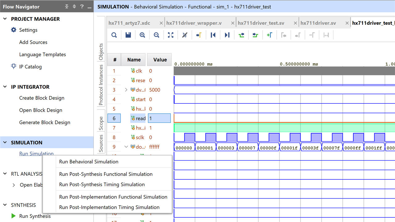
Then from the Flow Navigator, we click Run Simulation and select a simulation type to invoke the Vivado simulator workspace.
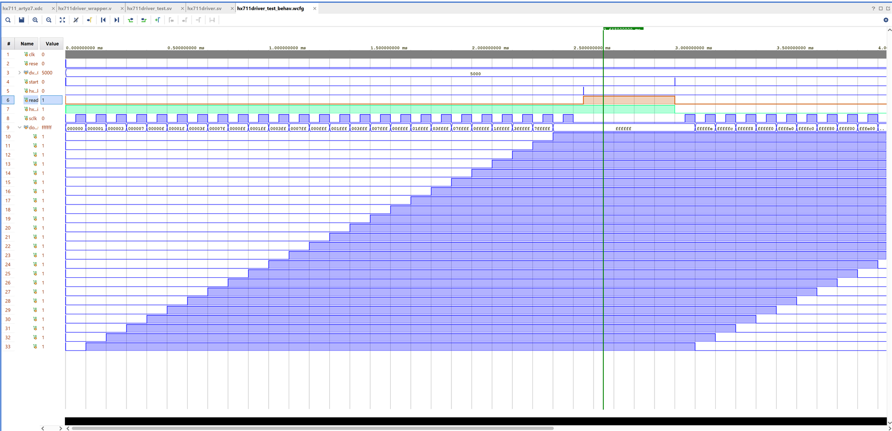
The diagram shows the two actions readings of our test bench. First, reading the FFFFFFh value, then the 000000h value, with MSB first. Data received by the serial input is shifted to the left as it comes by the line. While reading, the ready signal is low, and when data is ready, it goes high. The reading is triggered when the start signal goes high and the in signal is low. While the in signal is high, the HX711 module isn't ready.
Testing the hx711 driver with the module
Once the HX711 driver circuit was tested in simulation, I moved on to testing the driver with an HX711 module to verify its correct implementation. For this, I generated the following diagram from the Vivado block designer.

Key points of the diagram include:
- The clocking wizard to generate the clock signal.
- The Processor System Reset to manage the module reset signal.
- A Verilog wrapper of the driver written in SystemVerilog, as the Vivado block designer can only recognize RTL blocks written in VHDL or SystemVerilog.
- A constant block to adjust the divider that adjusts half of the clock signal for communication with the HX711 module, a variant of SPI serial communication
- Inputs and outputs to the outside, including:
- two push buttons on the board to force the reset and start signal,
- a digital input to receive data from the HX711,
- a digital output for the clock signal or serial communication control,
- and two LEDs for signaling readiness and completion.
- An integrated IP logic analyzer block to debug the signals from Vivado.
Wrapping the SystemVerilog Module for Vivado Integration
To integrate our SystemVerilog HX711 driver into a Vivado block design, we'll create a simple Verilog wrapper. This wrapper module will instantiate the SystemVerilog driver and expose its input and output ports to the block design environment. The process is straightforward: we just create a new Verilog module that instantiates the SystemVerilog driver and connects the input and output ports.
Once the wrapper is complete, we can incorporate it into a Vivado block design as an RTL module. This lets us combine the HX711 driver with other IP cores to generate a hardware design. In subsequent steps, we'll convert this module into an AXI-Lite IP block, enabling seamless communication between the FPGA and the Zynq ARM processor. This allows us to control the driver and retrieve weight data from the software.
`timescale 1ns / 1ps

module hx711driver_wrapper (
    input clk,
    input reset,
    input [15:0] dvsr,
    input start,
    output [23:0] dout,
    output hx711_done_tick,
    output ready,
    output sclk,
    input hx711_in
);

 // instantiate SystemVerilog driver
 hx711driver driver(
    .clk(clk),
    .reset(reset),
    .dvsr(dvsr),
    .start(start),
    .dout(dout),
    .hx711_done_tick(hx711_done_tick),
    .ready(ready),
    .hx711_in(hx711_in),
    .sclk(sclk)
 );


endmodule
Generating the Block Design Wrapper
To transform our block design into a synthesizable hardware module, we'll generate a design wrapper. Vivado provides a convenient way to automate this process with a single click. This wrapper module encapsulates the entire block design, including the HX711 driver and any other IP cores, making it ready for synthesis and implementation.
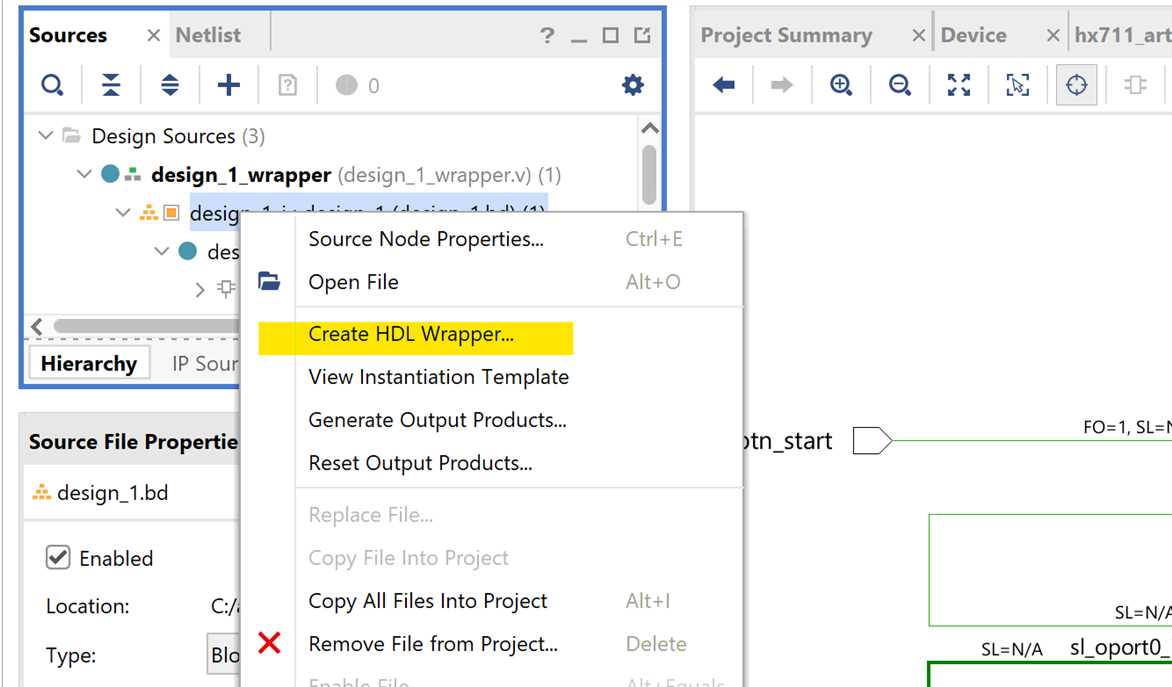
Assigning Pin Constraints
To ensure correct functionality, we'll create a constraints file to map the input and output signals of our block design to specific pins on the Arty Z7 FPGA board. This file will specify:
- Clock Signal: The clock signal that will drive the timing of our circuit.
- Input Signals: The push buttons on the board that will trigger specific actions.
- Output Signals: The LEDs that will provide visual feedback.
- HX711 Interface: The input and output signals for serial communication with the HX711 module, including the clock and data lines.
## hx711 driver, test bench constraints

## Clock Signal
set_property -dict { PACKAGE_PIN H16    IOSTANDARD LVCMOS33 } [get_ports { clk }]; #IO_L13P_T2_MRCC_35 Sch=SYSCLK
create_clock -add -name sys_clk_pin -period 10.00 -waveform {0 5} [get_ports { clk }];#set

## start button BTN0 D19
set_property PACKAGE_PIN D19 [get_ports btn_start]
set_property IOSTANDARD LVCMOS33 [get_ports btn_start]

## reset button
set_property IOSTANDARD LVCMOS33 [get_ports reset_rtl]
set_property PACKAGE_PIN D20 [get_ports reset_rtl]


## ChipKit Outer Digital Header
## hx711 data in #IO_L5P_T0_34            Sch=CK_IO0
set_property IOSTANDARD LVCMOS33 [get_ports h711_din]
set_property PACKAGE_PIN T14 [get_ports h711_din]


## signal clock  #IO_L2N_T0_34            Sch=CK_IO1
set_property IOSTANDARD LVCMOS33 [get_ports sclk_out]
set_property PACKAGE_PIN U12 [get_ports sclk_out]

## Done tick signal interrupt  #IO_L6N_T0_VREF_34 Sch=LED0
set_property IOSTANDARD LVCMOS33 [get_ports hx711_done_tick_led]
set_property PACKAGE_PIN R14 [get_ports hx711_done_tick_led]

## Data Ready Signal #IO_L6P_T0_34 Sch=LED1
set_property IOSTANDARD LVCMOS33 [get_ports ready_led]
set_property PACKAGE_PIN P14 [get_ports ready_led]
While it's possible to manually write constraints, Vivado offers a user-friendly graphical interface to simplify the process. This interface allows us to visually assign input and output signals to specific FPGA pins and check for potential conflicts or undefined constraints. The image below illustrates how this tool can be used to configure the pin assignments for our design.

The accompanying image illustrates the final test setup. The HX711 ADC converter is connected to the digital input/output pins of the Arty Z7 FPGA board, while the load cell is interfaced with the analog input pins of the HX711. This configuration allows the FPGA to communicate with the HX711 and acquire weight measurements from the load cell.

Additionally, the Analog Discovery 2's logic analyzer was used to monitor the signal and data transmission between the HX711 and the Arty Z7.
Pressing the BTN0 push button triggers the start signal, initiating a new measurement cycle. If the HX711 module signals that new data is ready by pulling the OUT line low, the state machine begins generating clock pulses to read the 24-bit sample data.
Digilent waveforms logic analyzer

Creating an AXI-Lite IP block for the driver
To integrate the FPGA-based HX711 driver with the PYNQ framework, we'll use the AXI-Lite protocol. This simplified version of AXI is perfect for low-bandwidth control and status signals, providing a standardized interface for communication between the FPGA and the PYNQ processing system.
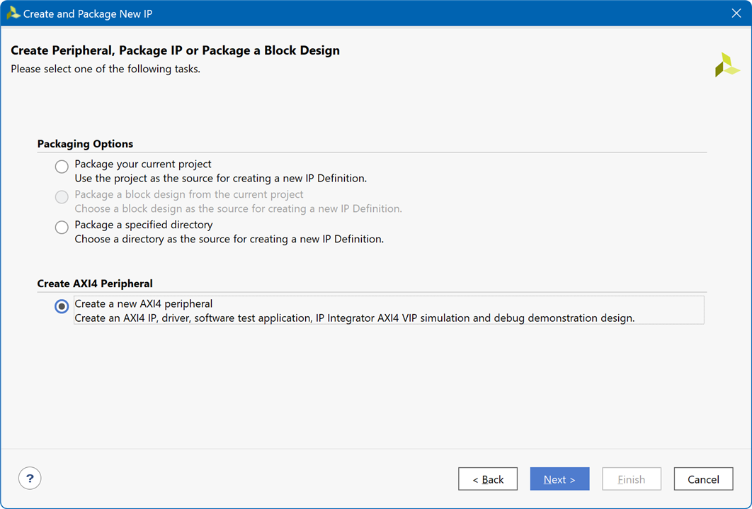
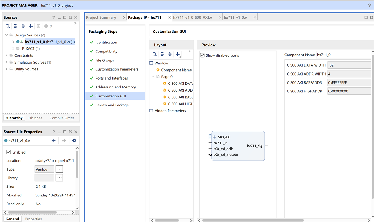
Vivado simplifies the creation of AXI-Lite IP cores with a dedicated wizard. This tool automates template generation, allowing designers to focus on defining input/output port interfaces and implementing the necessary logic. The following images illustrate the step-by-step process of using this wizard
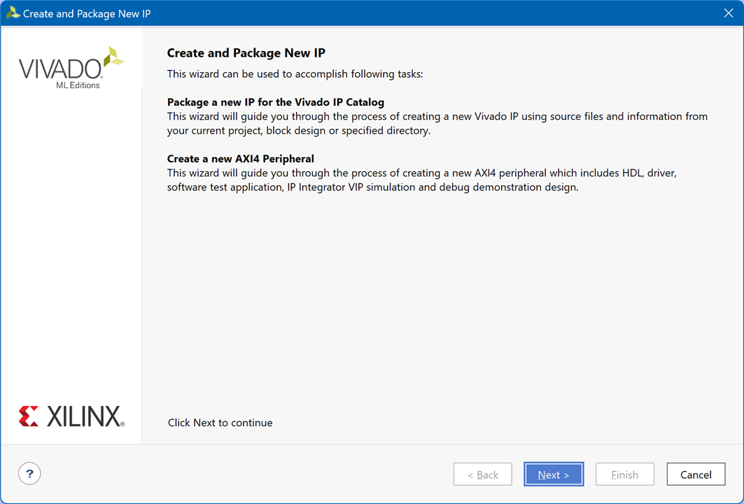
We want to create an AXI4 Lite Peripheral
Then define your interfaces. We will use 4x32 bits registers for simplicity:
- 0x00 Output - Start signal (1 bit)
- 0x04 Input - Read Data (24 bits)
- 0x08 Input - Data Ready Signal (1 bit)
- 0x0C Input - Done Signal (1 bit)

The wizard generates a new IP block, which can be further customized in a separate project.
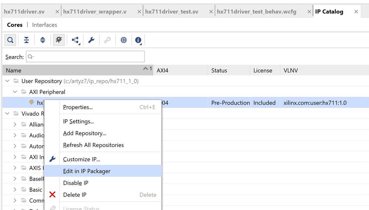
For an AXI4-Lite IP project, there are two Verilog files generated:
- <peripheral_name>.v (the top level file)
- <peripheral_name>_S00_AXI.v
We need to add our module sources
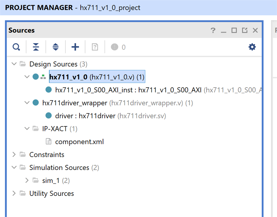
Next, we need to add our Verilog and SystemVerilog sources and modify the two generated templates.
Add the input ports and instantiate our top module and wire it to the AXI Lite wrapper.
`timescale 1 ns / 1 ps

	module hx711_v1_0_S00_AXI #
	(
		// Users to add parameters here

		// User parameters ends
		// Do not modify the parameters beyond this line

		// Width of S_AXI data bus
		parameter integer C_S_AXI_DATA_WIDTH	= 32,
		// Width of S_AXI address bus
		parameter integer C_S_AXI_ADDR_WIDTH	= 4
	)
	(
		// Users to add ports here
        input wire hx711_in,
        output wire hx711_sig,
		// User ports ends
		// Do not modify the ports beyond this line

		// Global Clock Signal
		input wire  S_AXI_ACLK,
		// Global Reset Signal. This Signal is Active LOW
		input wire  S_AXI_ARESETN,
		// Write address (issued by master, acceped by Slave)
		input wire [C_S_AXI_ADDR_WIDTH-1 : 0] S_AXI_AWADDR,
		// Write channel Protection type. This signal indicates the
    		// privilege and security level of the transaction, and whether
    		// the transaction is a data access or an instruction access.
		input wire [2 : 0] S_AXI_AWPROT,
		// Write address valid. This signal indicates that the master signaling
    		// valid write address and control information.
		input wire  S_AXI_AWVALID,
		// Write address ready. This signal indicates that the slave is ready
    		// to accept an address and associated control signals.
		output wire  S_AXI_AWREADY,
		// Write data (issued by master, acceped by Slave)
		input wire [C_S_AXI_DATA_WIDTH-1 : 0] S_AXI_WDATA,
		// Write strobes. This signal indicates which byte lanes hold
    		// valid data. There is one write strobe bit for each eight
    		// bits of the write data bus.
		input wire [(C_S_AXI_DATA_WIDTH/8)-1 : 0] S_AXI_WSTRB,
		// Write valid. This signal indicates that valid write
    		// data and strobes are available.
		input wire  S_AXI_WVALID,
		// Write ready. This signal indicates that the slave
    		// can accept the write data.
		output wire  S_AXI_WREADY,
		// Write response. This signal indicates the status
    		// of the write transaction.
		output wire [1 : 0] S_AXI_BRESP,
		// Write response valid. This signal indicates that the channel
    		// is signaling a valid write response.
		output wire  S_AXI_BVALID,
		// Response ready. This signal indicates that the master
    		// can accept a write response.
		input wire  S_AXI_BREADY,
		// Read address (issued by master, acceped by Slave)
		input wire [C_S_AXI_ADDR_WIDTH-1 : 0] S_AXI_ARADDR,
		// Protection type. This signal indicates the privilege
    		// and security level of the transaction, and whether the
    		// transaction is a data access or an instruction access.
		input wire [2 : 0] S_AXI_ARPROT,
		// Read address valid. This signal indicates that the channel
    		// is signaling valid read address and control information.
		input wire  S_AXI_ARVALID,
		// Read address ready. This signal indicates that the slave is
    		// ready to accept an address and associated control signals.
		output wire  S_AXI_ARREADY,
		// Read data (issued by slave)
		output wire [C_S_AXI_DATA_WIDTH-1 : 0] S_AXI_RDATA,
		// Read response. This signal indicates the status of the
    		// read transfer.
		output wire [1 : 0] S_AXI_RRESP,
		// Read valid. This signal indicates that the channel is
    		// signaling the required read data.
		output wire  S_AXI_RVALID,
		// Read ready. This signal indicates that the master can
    		// accept the read data and response information.
		input wire  S_AXI_RREADY
	);

	// AXI4LITE signals
	reg [C_S_AXI_ADDR_WIDTH-1 : 0] 	axi_awaddr;
	reg  	axi_awready;
	reg  	axi_wready;
	reg [1 : 0] 	axi_bresp;
	reg  	axi_bvalid;
	reg [C_S_AXI_ADDR_WIDTH-1 : 0] 	axi_araddr;
	reg  	axi_arready;
	reg [C_S_AXI_DATA_WIDTH-1 : 0] 	axi_rdata;
	reg [1 : 0] 	axi_rresp;
	reg  	axi_rvalid;

	// Example-specific design signals
	// local parameter for addressing 32 bit / 64 bit C_S_AXI_DATA_WIDTH
	// ADDR_LSB is used for addressing 32/64 bit registers/memories
	// ADDR_LSB = 2 for 32 bits (n downto 2)
	// ADDR_LSB = 3 for 64 bits (n downto 3)
	localparam integer ADDR_LSB = (C_S_AXI_DATA_WIDTH/32) + 1;
	localparam integer OPT_MEM_ADDR_BITS = 1;
	//----------------------------------------------
	//-- Signals for user logic register space example
	//------------------------------------------------
	//-- Number of Slave Registers 4
	reg [C_S_AXI_DATA_WIDTH-1:0]	slv_reg0;
	wire [C_S_AXI_DATA_WIDTH-1:0]	slv_reg1;
	wire [C_S_AXI_DATA_WIDTH-1:0]	slv_reg2;
	wire [C_S_AXI_DATA_WIDTH-1:0]	slv_reg3;
	wire	 slv_reg_rden;
	wire	 slv_reg_wren;
	reg [C_S_AXI_DATA_WIDTH-1:0]	 reg_data_out;
	integer	 byte_index;
	reg	 aw_en;

	// I/O Connections assignments

	assign S_AXI_AWREADY	= axi_awready;
	assign S_AXI_WREADY	= axi_wready;
	assign S_AXI_BRESP	= axi_bresp;
	assign S_AXI_BVALID	= axi_bvalid;
	assign S_AXI_ARREADY	= axi_arready;
	assign S_AXI_RDATA	= axi_rdata;
	assign S_AXI_RRESP	= axi_rresp;
	assign S_AXI_RVALID	= axi_rvalid;
	// Implement axi_awready generation
	// axi_awready is asserted for one S_AXI_ACLK clock cycle when both
	// S_AXI_AWVALID and S_AXI_WVALID are asserted. axi_awready is
	// de-asserted when reset is low.

	always @( posedge S_AXI_ACLK )
	begin
	  if ( S_AXI_ARESETN == 1'b0 )
	    begin
	      axi_awready <= 1'b0;
	      aw_en <= 1'b1;
	    end
	  else
	    begin
	      if (~axi_awready && S_AXI_AWVALID && S_AXI_WVALID && aw_en)
	        begin
	          // slave is ready to accept write address when
	          // there is a valid write address and write data
	          // on the write address and data bus. This design
	          // expects no outstanding transactions.
	          axi_awready <= 1'b1;
	          aw_en <= 1'b0;
	        end
	        else if (S_AXI_BREADY && axi_bvalid)
	            begin
	              aw_en <= 1'b1;
	              axi_awready <= 1'b0;
	            end
	      else
	        begin
	          axi_awready <= 1'b0;
	        end
	    end
	end

	// Implement axi_awaddr latching
	// This process is used to latch the address when both
	// S_AXI_AWVALID and S_AXI_WVALID are valid.

	always @( posedge S_AXI_ACLK )
	begin
	  if ( S_AXI_ARESETN == 1'b0 )
	    begin
	      axi_awaddr <= 0;
	    end
	  else
	    begin
	      if (~axi_awready && S_AXI_AWVALID && S_AXI_WVALID && aw_en)
	        begin
	          // Write Address latching
	          axi_awaddr <= S_AXI_AWADDR;
	        end
	    end
	end

	// Implement axi_wready generation
	// axi_wready is asserted for one S_AXI_ACLK clock cycle when both
	// S_AXI_AWVALID and S_AXI_WVALID are asserted. axi_wready is
	// de-asserted when reset is low.

	always @( posedge S_AXI_ACLK )
	begin
	  if ( S_AXI_ARESETN == 1'b0 )
	    begin
	      axi_wready <= 1'b0;
	    end
	  else
	    begin
	      if (~axi_wready && S_AXI_WVALID && S_AXI_AWVALID && aw_en )
	        begin
	          // slave is ready to accept write data when
	          // there is a valid write address and write data
	          // on the write address and data bus. This design
	          // expects no outstanding transactions.
	          axi_wready <= 1'b1;
	        end
	      else
	        begin
	          axi_wready <= 1'b0;
	        end
	    end
	end

	// Implement memory mapped register select and write logic generation
	// The write data is accepted and written to memory mapped registers when
	// axi_awready, S_AXI_WVALID, axi_wready and S_AXI_WVALID are asserted. Write strobes are used to
	// select byte enables of slave registers while writing.
	// These registers are cleared when reset (active low) is applied.
	// Slave register write enable is asserted when valid address and data are available
	// and the slave is ready to accept the write address and write data.
	assign slv_reg_wren = axi_wready && S_AXI_WVALID && axi_awready && S_AXI_AWVALID;

	always @( posedge S_AXI_ACLK )
	begin
	  if ( S_AXI_ARESETN == 1'b0 )
	    begin
	      slv_reg0 <= 0;
	      // slv_reg1 <= 0;
	      // slv_reg2 <= 0;
	      // slv_reg3 <= 0;
	    end
	  else begin
	    if (slv_reg_wren)
	      begin
	        case ( axi_awaddr[ADDR_LSB+OPT_MEM_ADDR_BITS:ADDR_LSB] )
	          2'h0:
	            for ( byte_index = 0; byte_index <= (C_S_AXI_DATA_WIDTH/8)-1; byte_index = byte_index+1 )
	              if ( S_AXI_WSTRB[byte_index] == 1 ) begin
	                // Respective byte enables are asserted as per write strobes
	                // Slave register 0
	                slv_reg0[(byte_index*8) +: 8] <= S_AXI_WDATA[(byte_index*8) +: 8];
	              end
	          2'h1:
	            for ( byte_index = 0; byte_index <= (C_S_AXI_DATA_WIDTH/8)-1; byte_index = byte_index+1 )
	              if ( S_AXI_WSTRB[byte_index] == 1 ) begin
	                // Respective byte enables are asserted as per write strobes
	                // Slave register 1
	                // slv_reg1[(byte_index*8) +: 8] <= S_AXI_WDATA[(byte_index*8) +: 8];
	              end
	          2'h2:
	            for ( byte_index = 0; byte_index <= (C_S_AXI_DATA_WIDTH/8)-1; byte_index = byte_index+1 )
	              if ( S_AXI_WSTRB[byte_index] == 1 ) begin
	                // Respective byte enables are asserted as per write strobes
	                // Slave register 2
	                // slv_reg2[(byte_index*8) +: 8] <= S_AXI_WDATA[(byte_index*8) +: 8];
	              end
	          2'h3:
	            for ( byte_index = 0; byte_index <= (C_S_AXI_DATA_WIDTH/8)-1; byte_index = byte_index+1 )
	              if ( S_AXI_WSTRB[byte_index] == 1 ) begin
	                // Respective byte enables are asserted as per write strobes
	                // Slave register 3
	                // slv_reg3[(byte_index*8) +: 8] <= S_AXI_WDATA[(byte_index*8) +: 8];
	              end
	          default : begin
	                      slv_reg0 <= slv_reg0;
	                      // slv_reg1 <= slv_reg1;
	                      // slv_reg2 <= slv_reg2;
	                      // slv_reg3 <= slv_reg3;
	                    end
	        endcase
	      end
	  end
	end

	// Implement write response logic generation
	// The write response and response valid signals are asserted by the slave
	// when axi_wready, S_AXI_WVALID, axi_wready and S_AXI_WVALID are asserted.
	// This marks the acceptance of address and indicates the status of
	// write transaction.

	always @( posedge S_AXI_ACLK )
	begin
	  if ( S_AXI_ARESETN == 1'b0 )
	    begin
	      axi_bvalid  <= 0;
	      axi_bresp   <= 2'b0;
	    end
	  else
	    begin
	      if (axi_awready && S_AXI_AWVALID && ~axi_bvalid && axi_wready && S_AXI_WVALID)
	        begin
	          // indicates a valid write response is available
	          axi_bvalid <= 1'b1;
	          axi_bresp  <= 2'b0; // 'OKAY' response
	        end                   // work error responses in future
	      else
	        begin
	          if (S_AXI_BREADY && axi_bvalid)
	            //check if bready is asserted while bvalid is high)
	            //(there is a possibility that bready is always asserted high)
	            begin
	              axi_bvalid <= 1'b0;
	            end
	        end
	    end
	end

	// Implement axi_arready generation
	// axi_arready is asserted for one S_AXI_ACLK clock cycle when
	// S_AXI_ARVALID is asserted. axi_awready is
	// de-asserted when reset (active low) is asserted.
	// The read address is also latched when S_AXI_ARVALID is
	// asserted. axi_araddr is reset to zero on reset assertion.

	always @( posedge S_AXI_ACLK )
	begin
	  if ( S_AXI_ARESETN == 1'b0 )
	    begin
	      axi_arready <= 1'b0;
	      axi_araddr  <= 32'b0;
	    end
	  else
	    begin
	      if (~axi_arready && S_AXI_ARVALID)
	        begin
	          // indicates that the slave has acceped the valid read address
	          axi_arready <= 1'b1;
	          // Read address latching
	          axi_araddr  <= S_AXI_ARADDR;
	        end
	      else
	        begin
	          axi_arready <= 1'b0;
	        end
	    end
	end

	// Implement axi_arvalid generation
	// axi_rvalid is asserted for one S_AXI_ACLK clock cycle when both
	// S_AXI_ARVALID and axi_arready are asserted. The slave registers
	// data are available on the axi_rdata bus at this instance. The
	// assertion of axi_rvalid marks the validity of read data on the
	// bus and axi_rresp indicates the status of read transaction.axi_rvalid
	// is deasserted on reset (active low). axi_rresp and axi_rdata are
	// cleared to zero on reset (active low).
	always @( posedge S_AXI_ACLK )
	begin
	  if ( S_AXI_ARESETN == 1'b0 )
	    begin
	      axi_rvalid <= 0;
	      axi_rresp  <= 0;
	    end
	  else
	    begin
	      if (axi_arready && S_AXI_ARVALID && ~axi_rvalid)
	        begin
	          // Valid read data is available at the read data bus
	          axi_rvalid <= 1'b1;
	          axi_rresp  <= 2'b0; // 'OKAY' response
	        end
	      else if (axi_rvalid && S_AXI_RREADY)
	        begin
	          // Read data is accepted by the master
	          axi_rvalid <= 1'b0;
	        end
	    end
	end

	// Implement memory mapped register select and read logic generation
	// Slave register read enable is asserted when valid address is available
	// and the slave is ready to accept the read address.
	assign slv_reg_rden = axi_arready & S_AXI_ARVALID & ~axi_rvalid;
	always @(*)
	begin
	      // Address decoding for reading registers
	      case ( axi_araddr[ADDR_LSB+OPT_MEM_ADDR_BITS:ADDR_LSB] )
	        2'h0   : reg_data_out <= slv_reg0;
	        2'h1   : reg_data_out <= slv_reg1;
	        2'h2   : reg_data_out <= slv_reg2;
	        2'h3   : reg_data_out <= slv_reg3;
	        default : reg_data_out <= 0;
	      endcase
	end

	// Output register or memory read data
	always @( posedge S_AXI_ACLK )
	begin
	  if ( S_AXI_ARESETN == 1'b0 )
	    begin
	      axi_rdata  <= 0;
	    end
	  else
	    begin
	      // When there is a valid read address (S_AXI_ARVALID) with
	      // acceptance of read address by the slave (axi_arready),
	      // output the read dada
	      if (slv_reg_rden)
	        begin
	          axi_rdata <= reg_data_out;     // register read data
	        end
	    end
	end

	// Add user logic here

	wire start;
	assign start = slv_reg0[1:0];

	wire [23:0] dout;
	wire hx711_done_tick;
	wire ready;
	assign slv_reg1 = {8'b0, dout};
	assign slv_reg2 = {31'b0, ready};
	assign slv_reg3 = {31'b0, hx711_done_tick};

     hx711driver driver(
        .clk(S_AXI_ACLK),
        .reset(!S_AXI_ARESETN),
        .dvsr(5000), // 10 kHz
        .start(start),
        .dout(dout),
        .hx711_done_tick(hx711_done_tick),
        .ready(ready),
        .hx711_in(hx711_in),
        .sclk(hx711_sig)
 );
	// User logic ends

	endmodule
Then modify the wrapper
`timescale 1 ns / 1 ps

	module hx711_v1_0 #
	(
		// Users to add parameters here

		// User parameters ends
		// Do not modify the parameters beyond this line


		// Parameters of Axi Slave Bus Interface S00_AXI
		parameter integer C_S00_AXI_DATA_WIDTH	= 32,
		parameter integer C_S00_AXI_ADDR_WIDTH	= 4
	)
	(
		// Users to add ports here
        input wire hx711_in,
        output wire hx711_sig,

		// User ports ends
		// Do not modify the ports beyond this line


		// Ports of Axi Slave Bus Interface S00_AXI
		input wire  s00_axi_aclk,
		input wire  s00_axi_aresetn,
		input wire [C_S00_AXI_ADDR_WIDTH-1 : 0] s00_axi_awaddr,
		input wire [2 : 0] s00_axi_awprot,
		input wire  s00_axi_awvalid,
		output wire  s00_axi_awready,
		input wire [C_S00_AXI_DATA_WIDTH-1 : 0] s00_axi_wdata,
		input wire [(C_S00_AXI_DATA_WIDTH/8)-1 : 0] s00_axi_wstrb,
		input wire  s00_axi_wvalid,
		output wire  s00_axi_wready,
		output wire [1 : 0] s00_axi_bresp,
		output wire  s00_axi_bvalid,
		input wire  s00_axi_bready,
		input wire [C_S00_AXI_ADDR_WIDTH-1 : 0] s00_axi_araddr,
		input wire [2 : 0] s00_axi_arprot,
		input wire  s00_axi_arvalid,
		output wire  s00_axi_arready,
		output wire [C_S00_AXI_DATA_WIDTH-1 : 0] s00_axi_rdata,
		output wire [1 : 0] s00_axi_rresp,
		output wire  s00_axi_rvalid,
		input wire  s00_axi_rready
	);
// Instantiation of Axi Bus Interface S00_AXI
	hx711_v1_0_S00_AXI # (
		.C_S_AXI_DATA_WIDTH(C_S00_AXI_DATA_WIDTH),
		.C_S_AXI_ADDR_WIDTH(C_S00_AXI_ADDR_WIDTH)
	) hx711_v1_0_S00_AXI_inst (
	    .hx711_in(hx711_in),
	    .hx711_sig(hx711_sig),
		.S_AXI_ACLK(s00_axi_aclk),
		.S_AXI_ARESETN(s00_axi_aresetn),
		.S_AXI_AWADDR(s00_axi_awaddr),
		.S_AXI_AWPROT(s00_axi_awprot),
		.S_AXI_AWVALID(s00_axi_awvalid),
		.S_AXI_AWREADY(s00_axi_awready),
		.S_AXI_WDATA(s00_axi_wdata),
		.S_AXI_WSTRB(s00_axi_wstrb),
		.S_AXI_WVALID(s00_axi_wvalid),
		.S_AXI_WREADY(s00_axi_wready),
		.S_AXI_BRESP(s00_axi_bresp),
		.S_AXI_BVALID(s00_axi_bvalid),
		.S_AXI_BREADY(s00_axi_bready),
		.S_AXI_ARADDR(s00_axi_araddr),
		.S_AXI_ARPROT(s00_axi_arprot),
		.S_AXI_ARVALID(s00_axi_arvalid),
		.S_AXI_ARREADY(s00_axi_arready),
		.S_AXI_RDATA(s00_axi_rdata),
		.S_AXI_RRESP(s00_axi_rresp),
		.S_AXI_RVALID(s00_axi_rvalid),
		.S_AXI_RREADY(s00_axi_rready)
	);

	// Add user logic here

	// User logic ends

	endmodule
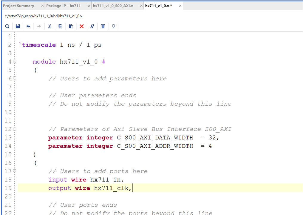
File hx711_v1_0.v add the two user ports inputs: m1_sensor and m1_sensor
- input wire hx711_in,
- output wire m2_hx711_clk,
Signal wiring:

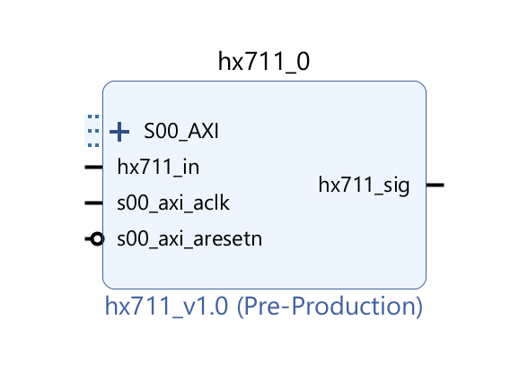
We can visualize the appearance of our IP block.
Creating a PYNQ Overlay with a Custom IP Block
Finally, we create a PYNQ overlay using our custom IP block for the Arty-Z7 FPGA board. We will use Vivado to combine our IP block with a hardware design, create a hardware description (HDL), and then package it as a PYNQ overlay. This will allow us to fully utilize our hardware design within the PYNQ framework.
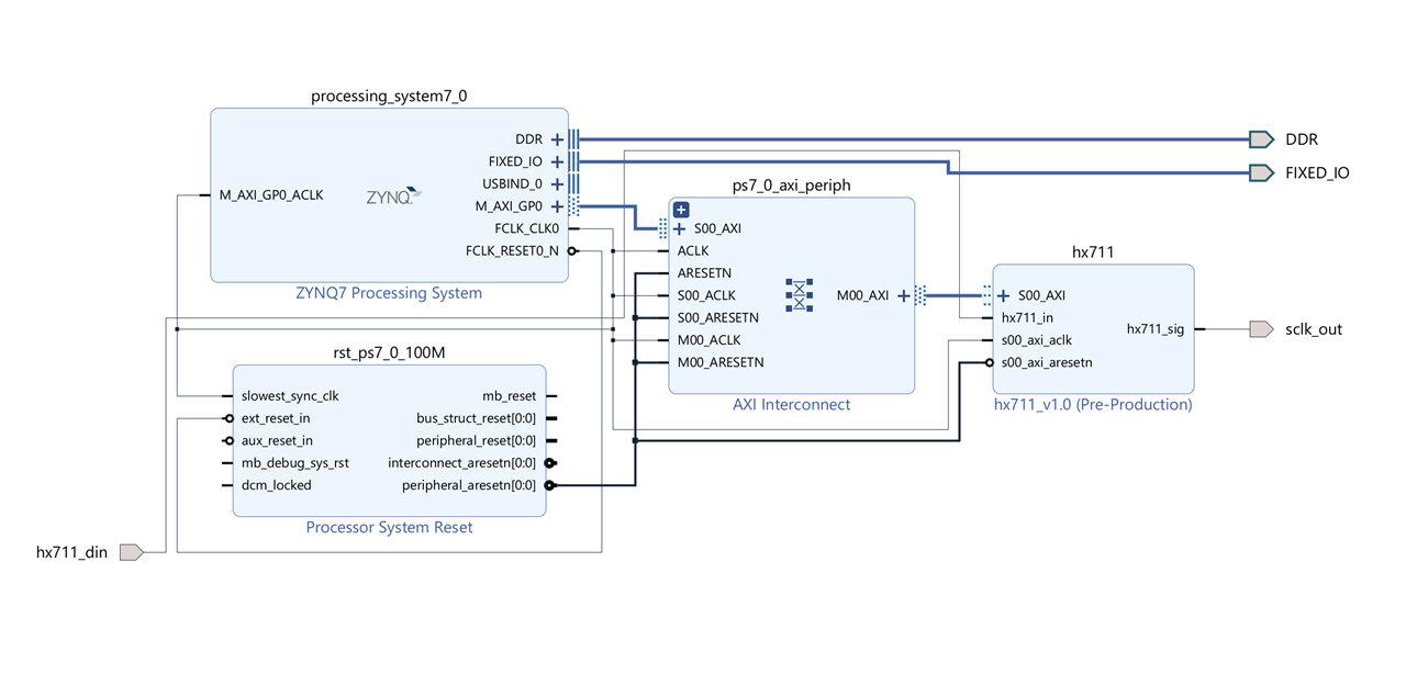
In the following video, I demonstrate how easy it is to create this design using the Vivado block editor. We only need to add the Zynq Processing System IP block and the AXI4 IP block we created for the driver to the diagram, and then run the connection automations.
As in the previous tests, we need to create the constraints file. In this case, it's much simpler because our circuit only exposes two ports to the outside: one input for the data and one output for the clock signal.
## ChipKit Outer Digital Header
## hx711 data in #IO_L5P_T0_34            Sch=CK_IO0
set_property IOSTANDARD LVCMOS33 [get_ports h711_din]
set_property PACKAGE_PIN T14 [get_ports h711_din]


## signal clock  #IO_L2N_T0_34            Sch=CK_IO1
set_property IOSTANDARD LVCMOS33 [get_ports sclk_out]
set_property PACKAGE_PIN U12 [get_ports sclk_out]
Again generate the block design wapper

And then we can generate and export the generated bitstream.
Copying Our New PYNQ Overlay to the Arty Z7
Transferring our overlay to the Arty Z7 is straightforward. We just need to locate and copy two files: the bitstream (.bit) and the metadata (.hwh), which informs the PYNQ framework about our overlay's structure. And then copy them to a folder where we have permissions. Note down the path, as you will need it to load the overlay from the Jupyter Notebook.

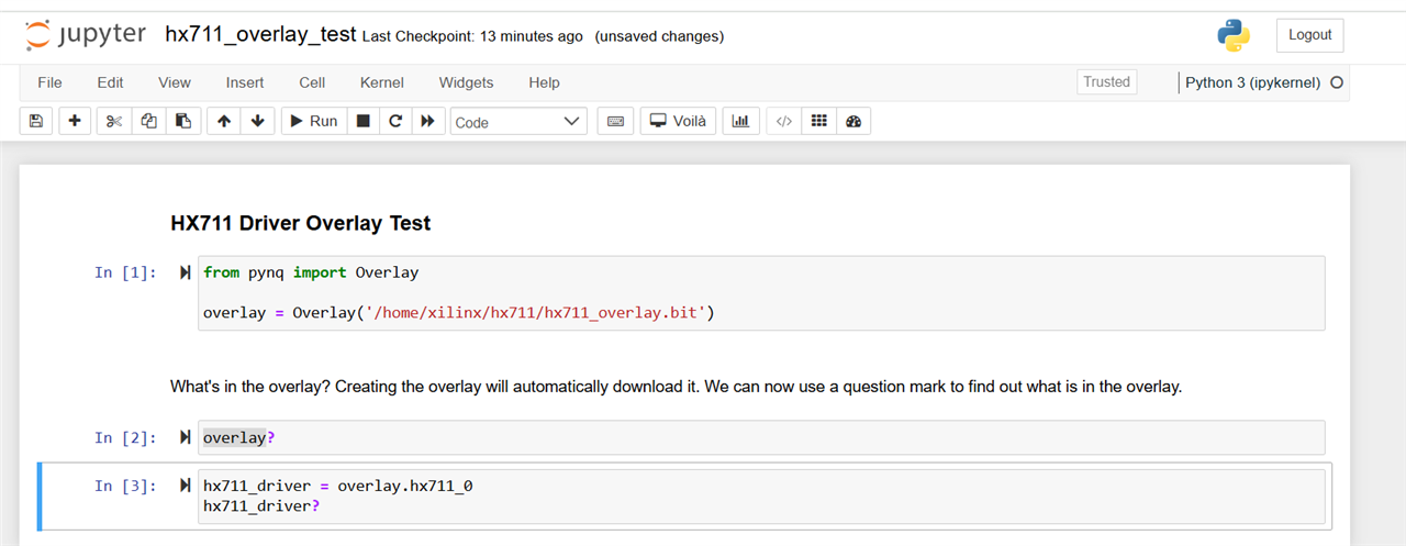
Alright, we're all set. Now, we can open a Jupyter Notebook, instantiate the overlay from Python, and use it to communicate with our HX711 driver.
Verifying the Implementation
To validate the functionality of the FPGA-based HX711 driver and its integration with PYNQ, we can use a logic analyzer to capture and analyze the signals on the FPGA board. By monitoring the clock, data, and control signals, we can verify that the driver is operating correctly and communicating with the HX711 sensor.
Additionally, we can write Python scripts to interact with the PYNQ overlay. These scripts can send commands to the driver, trigger data acquisition, and read the resulting measurements. By comparing the measured values with a reference scale, we can assess the accuracy and precision of the system.
I connected my Digilent Discovery 2 logical analyzer again and checked the signals when requesting new data from the driver using Python.
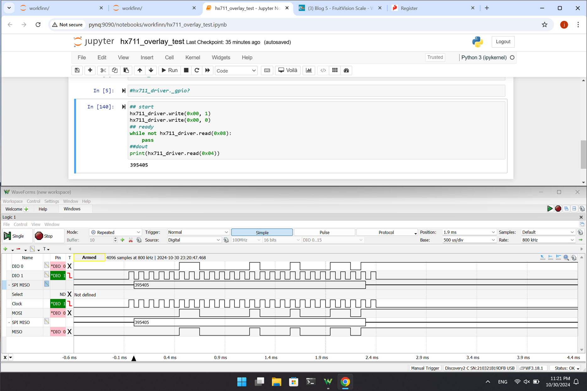
Example Python Code Snippet for Loading the HX711 Overlay
Below is a Python code snippet demonstrating how simple it is to load the new overlay and query the registers for the HX711 driver via the AXI4 Lite protocol:
#!/usr/bin/env python
# coding: utf-8

# ### HX711 Driver Overlay Test
# Registers
# Offset Description
# 0x00  Output - Start signal (1 bit)
# 0x04  Input  - Read Data (24 bits)
# 0x08  Input  - Data Ready Signal (1 bit)
# 0x0C  Input  - Done Signal (1 bit)
#

from pynq import Overlay

overlay = Overlay('/home/xilinx/hx711/hx711_overlay.bit')

hx711_driver = overlay.hx711

## reset start
hx711_driver.write(0x00, 0)

## start pulse
hx711_driver.write(0x00, 1)
hx711_driver.write(0x00, 0)

## wait until ready
while not hx711_driver.read(0x08):
    pass

## print dout
print(hx711_driver.read(0x04))
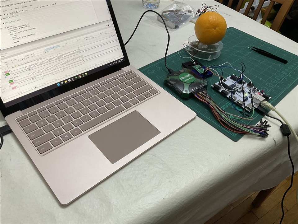
In the next image, I showcase my experimental setup. My laptop is running Digilent Waveforms, which displays the input and output signals exchanged between the Arty Z7 FPGA and the HX711 ADC module. Simultaneously, a Jupyter Notebook on the laptop executes Python code to interact with the HX711. The laptop is connected to the Digilent Discovery 2 multi-function instrument. The Arty Z7 FPGA is linked to the Ethernet LAN, enabling it to serve the Jupyter Notebook and communicate with the HX711 module. The HX711, in turn, samples the signals from a load cell that's currently measuring the weight of an orange.
Summary
In this post, I discussed the implementation of an HX711 controller using the FPGA fabric of the Zynq and its integration with a PYNQ overlay. The HX711, a 24-bit ADC specifically designed for scales, is used to sample analog signals from a load cell.
The FPGA-based controller employs a Finite State Machine (FSM) to manage the data acquisition process and timing. This controller is implemented in SystemVerilog and tested using a test bench. To enable communication with the ARM Zynq processor, I created an AXI-Lite IP block for control and data transfer.
The final setup involves the integration of the FPGA board, HX711, and load cell, along with a PYNQ overlay. Python scripts are used to interact with the controller and retrieve weight measurements.
References
- https://pynq.readthedocs.io/en/v2.1/overlay_design_methodology/overlay_tutorial.html
- HX711 24-Bit Analog-to-Digital Converter (ADC) for Weigh Scales
FruitVision Scale Blogs Series
- Blog 1 - FruitVision Scale - Digilent Arty Z7 - AMD Zynq-7000 - Overview
- Blog 2 - FruitVision Scale - PYNQ on the Digilent Arty Z7 - Quickstart
- Blog 3 - FruitVision Scale - Weighing strategies with load cells using the Digilent Arty Z7
- Blog 4 - FruitVision Scale - FPGA-Based HX711 Driver for Precision Weighing with AMD PYNQ
- Blog 5 - FruitVision Scale - Exploring Deep Learning Applications with AMD Zynq 7000
- Final - FruitVision Scale

