Introduction
Hello everyone! Welcome to my first post for the "The Eye on Intelligence" experimentation challenge. Thanks to element14 for selecting me as a participant. Throughout this challenge I will be attempting to build a smart fruit weighing system using the Digilent Arty Z7, courtesy of the generous support of AMD, the sponsor of this awesome challenge.
This blog post will introduce my FruitVisionScale project, detailing my objectives and the expected challenges. I will begin my development journey by exploring the Arty Z7's diverse features and capabilities. In my following post, I will explore the technical details further and share my early successes and problems.

Project Overview
My FruitVisionScale project aims to develop a real-time embedded vision system capable of accurately classifying and weighing various fruits. Using computer vision and machine learning, this system seeks to streamline the grocery store checkout process, reducing wait times and errors.
Key Goals
- Develop a real-time fruit classification system capable of accurately identifying various fruit types on-the-fly.
- Integrate precision load cells for exact weight measurement of fruits.
- Optimize the system for efficient operation on the Arty Z7 development board.
- Design an intuitive user interface to display fruit information and barcode data.
- Ensure smooth checkout by integrating with existing point-of-sale systems.
Introduction to the AMD Zynq-7000 (APSoC)
In this challenge, participants are required to design and develop an application utilizing the Digilent Arty Z7. The Arty Z7 is a development platform centered around the Zynq-7000 All Programmable System-on-Chip (AP SoC) from AMD. This architecture combines a dual-core, 650 MHz ARM Cortex-A9 processor with AMD 7-series Field Programmable Gate Array (FPGA) logic, comparable to the Artix-7 FPGA.
The Zynq-7000 All Programmable System-on-Chip (AP SoC) is an heterogeneous SoC. It combines various processing elements with programmable logic. These processing elements are implemented in silicon. The processing element acts as the master, booting up in the same manner as any other processor. This allows for highly optimized solutions to be implemented using both the processor and logic to leverage their inherent strengths.
What is an FPGA?
An FPGA is a flexible programmable chip that can be utilized to create custom-made digital circuits. It serves as a blank canvas that can be customized to meet specific requirements. In contrast to traditional digital chips with static circuits, an FPGA's design can be altered post-manufacture.
Designers can distribute their FPGA designs using hardware description languages such as VHDL, Verilog, or SystemVerilog. These descriptions are often encapsulated in IP (Intellectual Property) blocks, which streamline and democratize the process of circuit design with FPGAs. It is similar to having a collection of pre-assembled Lego blocks that can be combined to forge unique inventions.
FPGAs find applications in a diverse array of fields, including video game consoles, high-performance computing, artificial intelligence, and 5G wireless communications. FPGAs confer numerous advantages to system designers:
- Design Flexibility - enabling performance enhancements and upgrades.
- Reduction in NRE (Non-Recurring Engineering) costs.
- Reliability - Using one device instead of multiple discrete components enhances reliability by minimizing solder connections.
- Accelerated time-to-market.
- Maintainability - Some FPGAs can be updated in the field.
FPGA Architecture
An FPGA is composed of several key components:
- Configurable Logic Blocks (CLBs): These building blocks combine look-up tables (LUTs) and flip-flops to implement both combinatorial and sequential logic functions. LUTs are used for circuits where the output depends only on the current inputs, while flip-flops are used for circuits where the output depends on both the current inputs and the previous state.
- Interconnect Routing: This network of signal pathways connects the CLBs together, allowing them to communicate and interact.
- Input/Output (I/O) Blocks: These blocks provide the interface between the FPGA and external devices, enabling data input and output.
AMD Tools and Frameworks
AMD offers a variety of tools and frameworks to customize and develop your solutions:
- Vivado: A tool for designing, capturing, and implementing FPGA base platforms.
- Vitis / Vivado HLS: A high-level synthesis tool that supports C, C++, and OpenCL.
- Vitis IDE: An integrated development environment for embedded and accelerated software. Used to develop software solutions for MicroBlaze, Arm R5, A9, A53, and A72.
- Petalinux: Provides embedded Linux solutions.
- PYNQ: A Python framework for rapid prototyping on SoCs, RFSoCs, and Alveo.
- VitisAI: Facilitates the deployment of machine learning inference models using TensorFlow, Caffe, and PyTorch.
This post will explore testing Vivado and Vitis IDE through demo project solutions offered by Digilent for the Arty Z7 development board. In subsequent blogs, I aim to introduce Vitis HLS, PYQ, and VitisAI.
Vivado Overview
Vivado is a software tool for designing, capturing, and implementing FPGA-based platforms. It serves as the foundation of AMD's FPGA design flow, offering an all-encompassing environment for the creation and execution of FPGA-based designs.
Here's a brief summary of its key features:
- Unified Design Environment: Vivado acts as the cornerstone for all design and higher-level tools, providing a unified workspace for different design phases.
- HDL Support: It allows designers to express their designs using standard hardware description languages (HDLs), such as VHDL and Verilog.
- Extensive IP Library: Vivado is equipped with an extensive library of pre-designed Intellectual Property (IP) cores, which speeds up the development process and streamlines complex designs.
- Integration with Vitis HLS: Vivado integrates smoothly with Vitis High-Level Synthesis (HLS), enabling designers to use C/C++ code to create optimized RTL (Register Transfer Level) designs.
Vivado Flow Overview
This is the Vivado Flow:
- Synthesis: involves converting high-level HDL code into a netlist, which is an interconnected list of logic gates. It also optimizes the netlist for area, speed, and power consumption.
- Simulation: Vivado allows to simulate designs using the Vivado Simulator.
- Placement assigns physical locations to the logic gates within the FPGA, taking into account factors such as congestion and timing constraints.
- Routing connects the placed logic gates using the FPGA's internal wiring channels, ensuring that timing requirements are met and avoiding electrical shorts.
- Power estimation: Vivado can generate power estimations.
- Bitstream Generation creates a binary file that contains the FPGA's configuration data. This file is used to program the FPGA and implement the designed circuit.
The flow implementation settings can be managed using Constraints (XDC file) and implementation strategies.
Arty Z7 overview
The ZYNQ 7000-based board from Digilent is a versatile platform for embedded applications, merging a robust ARM processor with programmable logic. It is built around a 650MHz dual-core Cortex-A9 processor and a DDR3 memory controller, facilitating rapid data access. The board includes high-bandwidth peripheral controllers such as Gigabit Ethernet, USB 2.0, and SDIO for external device connectivity. Additionally, it offers SPI, UART, CAN, and I2C interfaces for lower-bandwidth applications.
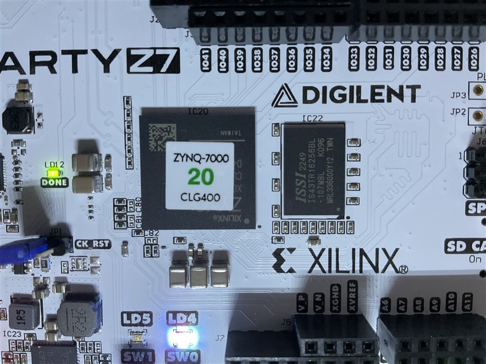
To facilitate flexible programming and configuration, the board supports multiple programming options, including JTAG, Quad-SPI flash, and microSD card. Additionally, the board includes programmable logic equivalent to an Artix-7 FPGA, allowing for custom hardware acceleration and design flexibility.
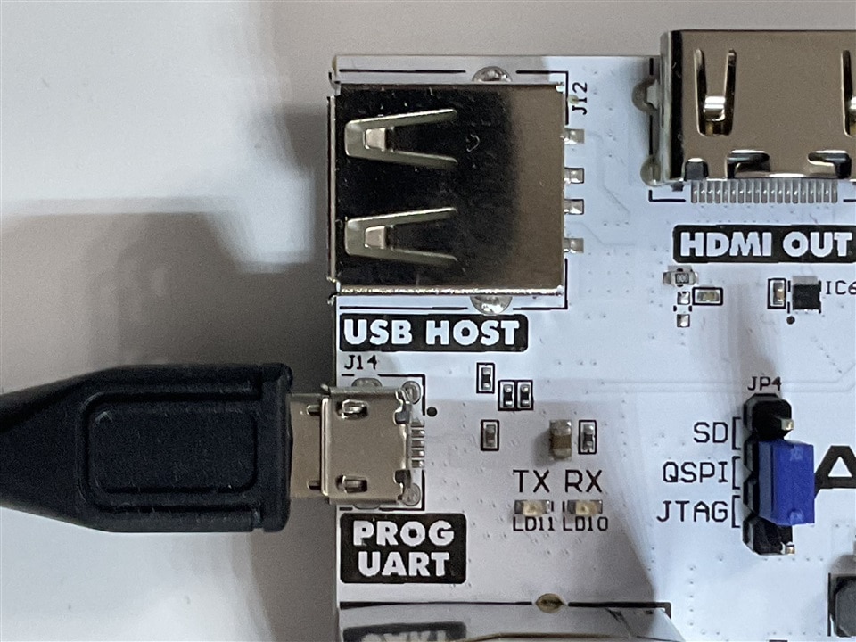
In terms of memory, the board features 512MB of DDR3 RAM for ample data storage and processing. A 16MB Quad-SPI Flash memory is pre-programmed with a unique identifier for device identification and authentication. Additionally, a microSD slot provides expandable storage capabilities.
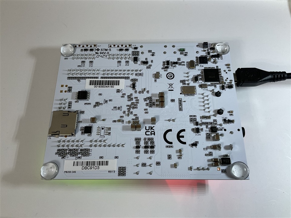
To power the board, users can choose between USB or an external 7V-15V power supply. For connectivity, the board includes a Gigabit Ethernet PHY, USB-JTAG programming circuitry, a USB-UART bridge, and a USB OTG PHY for host-only USB support.
Multimedia capabilities are also integrated, with an HDMI sink port for input and an HDMI source port for output. Additionally, a PWM-controlled mono audio output is available using a 3.5mm jack.
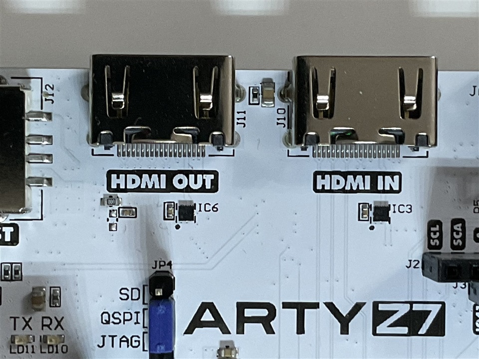
To interact with the board and expand its functionality, the board provides a user-friendly interface with 4 buttons, 2 slide switches, 4 LEDs, and 2 RGB LEDs. Additionally, two standard Pmod ports offer 16 total FPGA I/O, while an Arduino Shield connector provides access to up to 49 total FPGA I/O, including analog inputs for connecting sensors and other devices.
First Boot - Out of the box demo
The Arty Z7 Out-of-Box Demo provides a basic showcase of the board's capabilities, demonstrating the use of various peripherals including HDMI, audio, LEDs, buttons, and USB-UART.

Components needed for the demo:
- Arty Z7-20 development board
- HDMI-capable computer and monitor
- Two HDMI cables
- Serial terminal application (e.g., PuTTY, Tera Term
- Vivado with Vitis IDE
- MicroUSB Cable
- Power Supply
- Headphones or Speaker with 3.5 mm Audio Jack
LED Indicators
The two RGB LEDs cycle through red, green, blue, and white, while the user LEDs mirror the state of the user buttons. If only one user switch is activated, the LED states are inverted.
HDMI Pass-Through
Signals from the HDMI input port are forwarded to the HDMI output port, allowing for easy connection of external sources and displays.
Audio Output
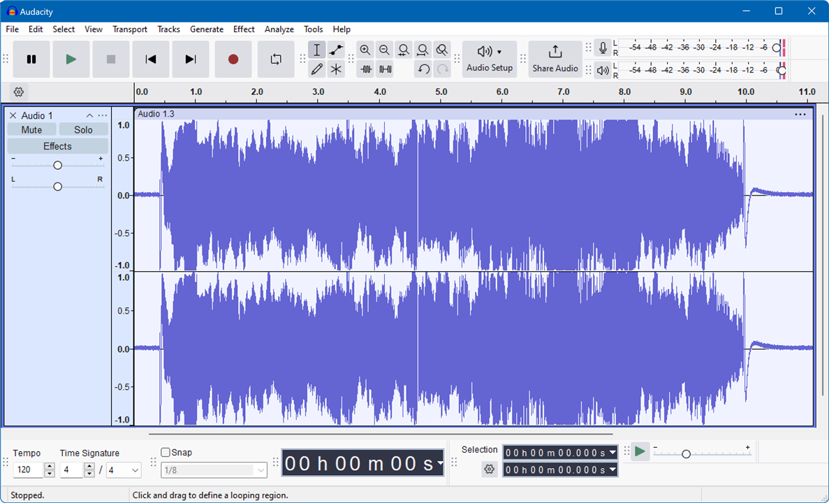
The Out of the Box Demo instructions indicated that pressing any button would generate a 261 Hz sine wave (C4) through the audio output jack for approximately 4.5 seconds. However, as a hidden feature, a classical melody would play instead of the expected C4 tone. The attached waveform captured by Audacity, WAV file, and video of my Multicom Pro handheld oscilloscope demonstrate the audio output from the Digilent Arty Z7 development board.
Serial Output:
Status messages are printed to a connected serial terminal via UART.
I used TeraTerm and connected it to the Arty Z7-20's serial port, using a baud rate of 115200.


Investigating Overheating Claims in the Arty-Z7
One common concern expressed in forums about the Digilent Arty-Z7 development board is its tendency to overheat. To empirically verify this claim, the board was left running for 20 minutes with the preloaded demo. Using Vivado's Logic Analyzer, the temperature of the Zynq7000 chip was monitored. The results showed a gradual increase in chip temperature from ambient temperature until reaching a steady state around 41°C, with an initial ambient temperature of 22°C.
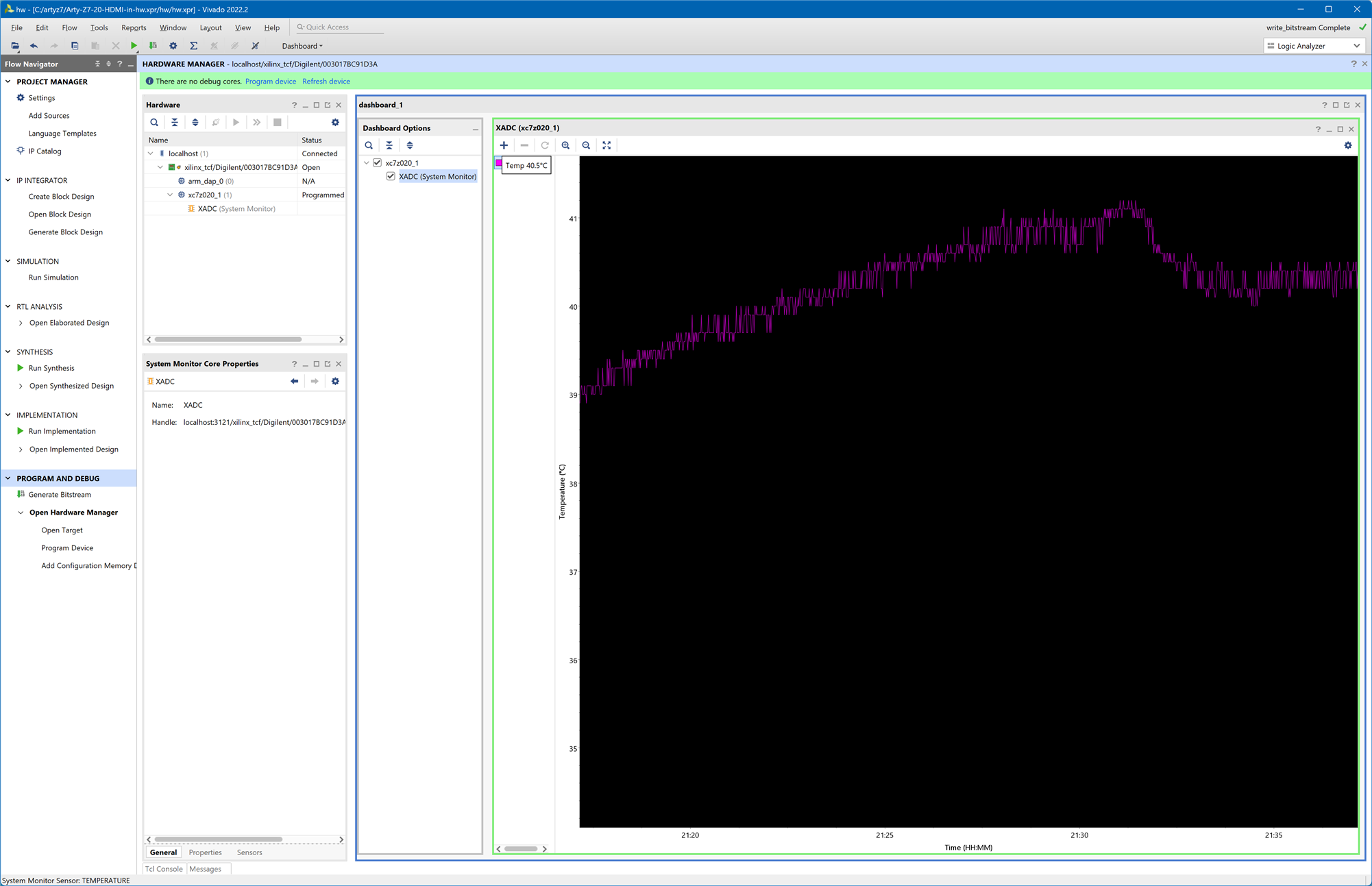
Vivado Hardware Manager, Logic Analyzer XADC System Monitor. Temperature.
During temperature monitoring, once stabilization was reached, I took this thermal image using a Fluke thermal imager.
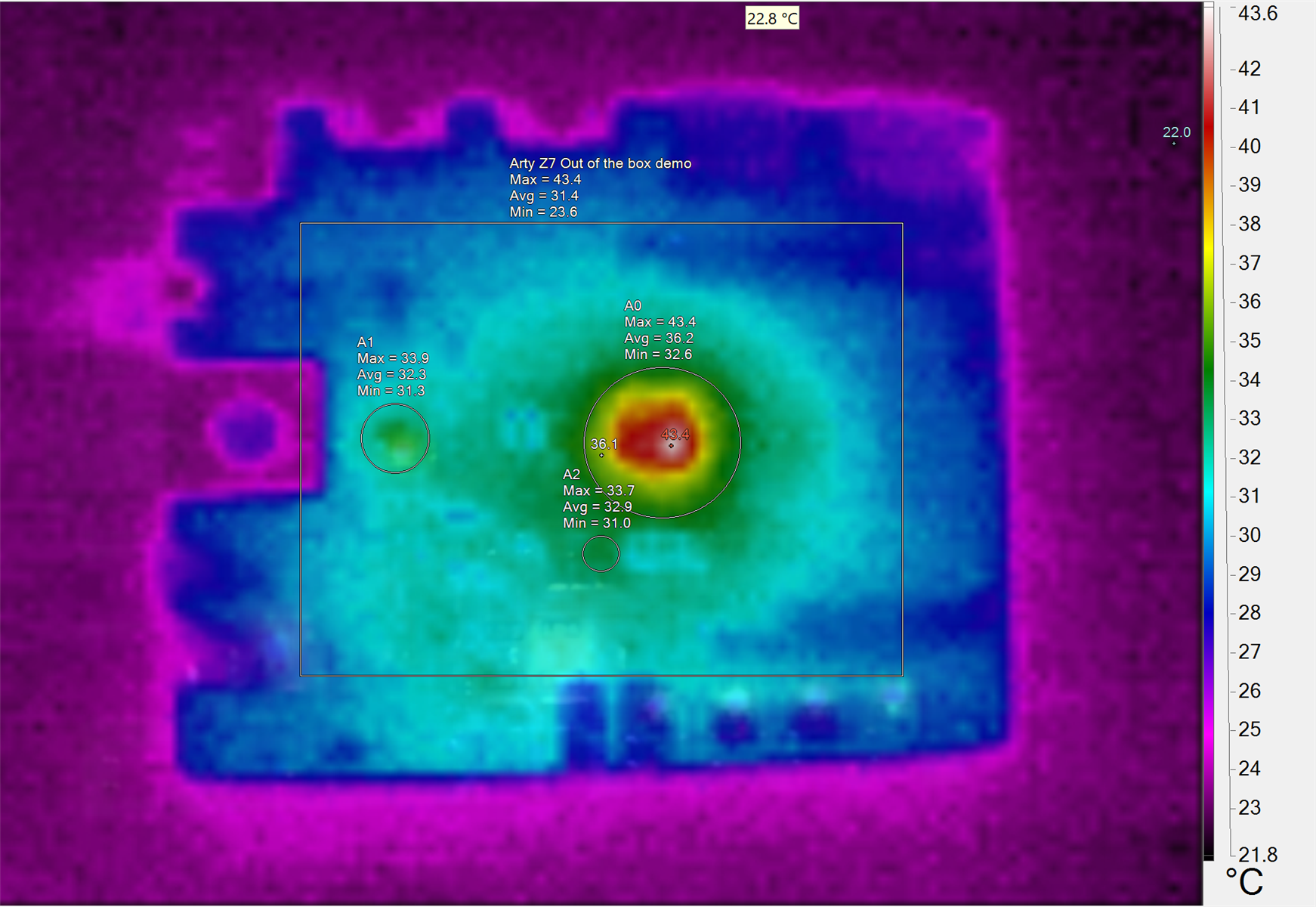
The image clearly shows the heat dissipated by the Zynq 7000 SoC and its surrounding temperature.
The hottest area (red and orange) corresponds to the Zynq 7000 SoC , confirming that it is the component dissipating the most heat.
A thermal gradient can be observed from the center (Zynq 7000) to the edges of the board, indicating that heat is being dissipated effectively, although the concentration in the chip is evident.
Components located near the Zynq7000 also show an increase in temperature, which is normal due to thermal conduction.
Based on the results of both experiments and considering that the Zynq 7000 chip in the Arty Z7 board is a commercial-grade model (0°C to 85°C), we can conclude that the board is operating within the thermal limits established by the manufacturer. The maximum temperature reached by the chip, around 43.4°C, is significantly below the specified upper limit.
Working with HDMI source and sink ports without a dedicated HDMI port
In this section, I'll explain how I configured a comfortable setup for working with HDMI source and sink ports, despite my laptop lacking a dedicated HDMI output or capture port.
The Setup
The setup consists of the following parts:
- Microsoft Surface Laptop
- StarTech.com Docking Station: This docking station adds an HDMI output for a display, two USB-A ports, a memory card reader, a USB-C port, an Ethernet RJ11 port, and a VGA output to your laptop.
- HDMI to USB Video Capture Dongle: This dongle allows you to capture HDMI video input and use it as a camera on your laptop.\
- Arty Z7 Board: The Arty acts as a second display for the laptop in extended mode and performs the HDMI passthrough demo.
Connections
- Connect the laptop to the StarTech.com Docking Station using the USB-C port.
- Connect the HDMI output of the docking station to the Arty Z7's HDMI IN port. This will configure the Arty Z7 as a second display for the laptop.
- Connect the Arty Z7's HDMI output to the HDMI to USB Video Capture Dongle. This will essentially turn the Arty Z7's HDMI output into a USB camera input for the laptop.
- The Arty Z7 is powered by the Surface Laptop unique USB port.
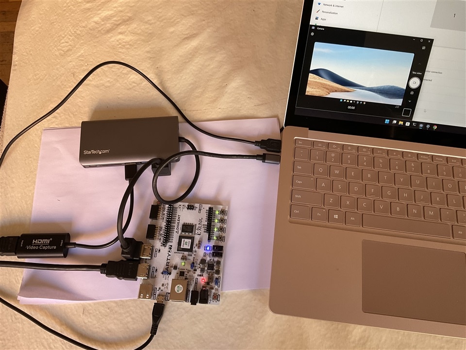
Video Demonstration
The video showcases the following key aspects of the setup:
- HDMI Source: An element14 video is played on the extended display, which is connected to the Arty Z7's HDMI IN port.
- HDMI Passthrough: The Arty Z7 processes the incoming HDMI signal and outputs it to its HDMI OUT port.
- Video Capture: The processed HDMI signal is captured by the HDMI to USB Video Capture dongle and displayed in real-time using the Windows Camera application in video mode.
- Thermal Imaging: A Fluke Thermal Imager captures the temperature of the Arty Z7's Zynq-7000 processor, which is shown to be 54 degrees Celsius during the demonstration.
This demonstration highlights the versatility of the Arty Z7 in handling HDMI signals. By combining HDMI passthrough and video capture capabilities, one can create a range of applications. The Arty Z7's ability to process HDMI signals in conjunction with its other features, such as FPGA programmability and ARM Cortex-A9 processor, makes it a valuable tool for a wide range of projects.
Understanding the example projects
Digilent provides several examples projects. I reviewed some of them:
Arty Z7 HDMI Input Demo
The Arty Z7 HDMI Input demo project shows the capabilities of the Arty Z7 board's HDMI ports. By receiving video data through the input port and transmitting it to the output port, the project demonstrates basic video processing functionality. Additionally, users can customize HDMI output settings using the UART interface and utilize multiple frame buffers for versatile video display and manipulation. The project offers various display options, such as changing resolution, selecting frame buffers, and applying effects like test patterns or color inversion. However, 1080p display output is not fully supported, and the input resolution is determined by the connected HDMI source, limiting direct control. For this demo project, when utilizing the HDMI output port, it is advised to power the Arty Z7 with a wall adapter to ensure the 5V signal complies with HDMI specifications. Although not specified in the reference manual, I have not encountered any issues powering the board via the USB port while using both the HDMI sink and source ports.
The Arty Z7 board features two HDMI ports: one for output (J11) and one for input (J10), both use HDMI type-A receptacles with the data and clock signals terminated and connected directly with the Zynq PL. Both ports are compatible with HDMI and DVI devices and use the TMDS signaling standard. The HDMI connectors include various signals such as data channels, clock channels, control buses, and a 5V power supply.
The Arty Z7's HDMI ports utilize transition-minimized differential signaling (TMDS) for high-speed digital video transmission. To effectively use these ports, a standard-compliant transmitter or receiver must be implemented in the Zynq PL. The Digilent GitHub repository offers ready-to-use reference IP for this purpose.
- dvi2rgb - This IP interfaces directly to raw transition-minimized differential signaling (TMDS) clock and data channel inputs as defined in DVI 1.0 specs for Sink devices. It decodes the video stream and outputs 24-bit RGB video data along with the pixel clock and synchronization signals
- rgb2dvi - This IP interfaces directly to raw transition-minimized differential signaling (TMDS) clock and data channel outputs as defined in DVI 1.0 specs for Source devices. It encodes 24-bit RGB video data along with the pixel clock and synchronization signals. More details about its
Auxiliary signals are used in the HDMI/DVI communication. The HPD pin indicates the presence of a ready sink, while the DDC bus enables communication between the display and graphics adapter. The DDC2B variant is based on I2C, with the source acting as the bus master and the sink as the bus slave. When a source detects a high level on the HPD pin, it queries the sink for video capabilities and initiates video transmission accordingly.
Additionally, the CEC protocol allows for control message exchange between devices on an HDMI chain. It is a one-wire protocol that operates at 3.3V and can be shared by multiple devices using an open-drain configuration.
https://digilent.com/reference/programmable-logic/arty-z7/demos/hdmi-input
Arty Z7 HDMI Input Demo Block Diagram Description
I've used Vivado 2022.2 and Vivado 2022.1 to open the provided project. If you get problems generating building the project review the synthesis settings for incorrect directories:
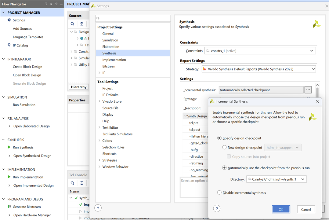
In the image the Interfaces View Diagram. Key points:
- DVI-to-RGB Video Decoder: Decodes DVI input into RGB data.
- Video In to AXI4-Stream: Converts RGB data to AXI4-Stream format.
- Input VTC: Generates timing signals for the input video.
- AXI VDMA: Handles data transfers between memory and processing blocks.
- Output VTC: Generates timing signals for the output video.
- AXI-4 Stream to Video Out: Converts AXI4-Stream data to parallel video output.
- RGB-to-DVI Video Encoder: Encodes RGB data into DVI format.
- DDC (Display Data Channel): Enables communication between display devices and graphics adapters.
- HPD (Hot Plug Detect): Signals the readiness of a display device to receive video data.

Block and signals description:
In the left of the diagram the Digilent DVI-to-RGB Video Decoder IP is a hardware module designed to decode DVI video streams and output the resulting RGB data, pixel clock, and synchronization signals. It directly interfaces with TMDS clock and data channels as specified in DVI 1.0 standards for sink devices.
In the right of the diagram the Digilent RGB-to-DVI Video Encoder IP is a hardware module that encodes RGB video data, pixel clock, and synchronization signals into TMDS format for DVI output. It directly interfaces with TMDS clock and data channels as defined in DVI 1.0 standards for source devices.
The Xilinx LogiCORE IP Video In to AXI4-Stream core acts as a bridge between video source (clocked parallel video data with synchronization signals - active video with either syncs, blanks or both) and video processing cores that use the AXI4-Stream Video Protocol. It converts video data with synchronization signals from the video source into the AXI4-Stream format. This core works in conjunction with the timing detector portion of the Xilinx Video Timing Controller (VTC) core.
The AXI VDMA core is an IP core that enables high-speed data transfer between memory and video peripherals using the AXI4-Stream protocol. It offers efficient two-dimensional DMA operations with separate read and write channels. Configuration, status, interrupt, and management settings are accessed through an AXI4-Lite interface.
The AXI-4 Stream to Video Out LogiCORE IP core converts AXI4-Stream signals into standard parallel video output signals with timing signals. It works with the AMD Video Timing Controller (VTC) core to generate the video format timing signals. The core is designed to be compatible with various external video sinks and provides standard video timing signals such as Vsync, Hsync, Vblank, Hblank, DE, and pixel clock. This allows to connect video processing blocks with an AXI4-Stream interface to an external video sink like a DVI PHY or the Digilent RGB-to-DVI Video Encoder IP as in this example.
The Processing System IP is a software interface for the Zynq 7000 Processing System. The Zynq 7000 family is an SoC that includes a processing system and a programmable logic unit. The Processing System IP Wrapper connects the PS and PL and helps integrate custom and embedded IPs using the Vivado IP integrator.
The HPD (Hot Plug Detect) pin is used by a display device (sink) to signal its readiness to receive video data. When the display is ready, it connects the 5V supply pin to the HPD pin. On the Arty Z7, this is achieved by driving the Hot Plug Assert signal high. However, this should only be done after a DDC channel slave has been implemented in the Zynq PL and is prepared to transmit display data.
The DDC (Display Data Channel) is a communication protocol between display devices (sinks) and graphics adapters (sources).
Constraints file
The flow implementation settings can be managed using Constraints (XDC file) and implementation strategies.
##HDMI RX Signals
set_property -dict { PACKAGE_PIN P19   IOSTANDARD TMDS_33  } [get_ports { TMDS_clk_n }]; #IO_L13N_T2_MRCC_34 Sch=HDMI_RX_CLK_N
create_clock -period 13.461 -waveform {0.000 6.73} [get_ports TMDS_clk_p]
set_property -dict { PACKAGE_PIN W20   IOSTANDARD TMDS_33  } [get_ports { TMDS_data_n[0]}]; #IO_L16N_T2_34 Sch=HDMI_RX_D0_N
set_property -dict { PACKAGE_PIN V20   IOSTANDARD TMDS_33  } [get_ports { TMDS_data_p[0]}]; #IO_L16P_T2_34 Sch=HDMI_RX_D0_P
set_property -dict { PACKAGE_PIN U20   IOSTANDARD TMDS_33  } [get_ports { TMDS_data_n[1]}]; #IO_L15N_T2_DQS_34 Sch=HDMI_RX_D1_N
set_property -dict { PACKAGE_PIN T20   IOSTANDARD TMDS_33  } [get_ports { TMDS_data_p[1]}]; #IO_L15P_T2_DQS_34 Sch=HDMI_RX_D1_P
set_property -dict { PACKAGE_PIN P20   IOSTANDARD TMDS_33  } [get_ports { TMDS_data_n[2]}]; #IO_L14N_T2_SRCC_34 Sch=HDMI_RX_D2_N
set_property -dict { PACKAGE_PIN N20   IOSTANDARD TMDS_33  } [get_ports { TMDS_data_p[2]}]; #IO_L14P_T2_SRCC_34 Sch=HDMI_RX_D2_P
set_property -dict { PACKAGE_PIN T19   IOSTANDARD LVCMOS33 } [get_ports { hdmi_hpd_tri_o[0] }]; #IO_25_34 Sch=HDMI_RX_HPD
set_property -dict { PACKAGE_PIN U14   IOSTANDARD LVCMOS33 } [get_ports { DDC_scl_io }]; #IO_L11P_T1_SRCC_34 Sch=HDMI_RX_SCL
set_property -dict { PACKAGE_PIN U15   IOSTANDARD LVCMOS33 } [get_ports { DDC_sda_io }]; #IO_L11N_T1_SRCC_34 Sch=HDMI_RX_SDA

##HDMI TX Signals
set_property -dict { PACKAGE_PIN L17   IOSTANDARD TMDS_33  } [get_ports { TMDS_1_clk_n }]; #IO_L11N_T1_SRCC_35 Sch=HDMI_TX_CLK_N
set_property -dict { PACKAGE_PIN L16   IOSTANDARD TMDS_33  } [get_ports { TMDS_1_clk_p }]; #IO_L11P_T1_SRCC_35 Sch=HDMI_TX_CLK_P
set_property -dict { PACKAGE_PIN K18   IOSTANDARD TMDS_33  } [get_ports { TMDS_1_data_n[0] }]; #IO_L12N_T1_MRCC_35 Sch=HDMI_TX_D0_N
set_property -dict { PACKAGE_PIN K17   IOSTANDARD TMDS_33  } [get_ports { TMDS_1_data_p[0]  }]; #IO_L12P_T1_MRCC_35 Sch=HDMI_TX_D0_P
set_property -dict { PACKAGE_PIN J19   IOSTANDARD TMDS_33  } [get_ports { TMDS_1_data_n[1]  }]; #IO_L10N_T1_AD11N_35 Sch=HDMI_TX_D1_N
set_property -dict { PACKAGE_PIN K19   IOSTANDARD TMDS_33  } [get_ports { TMDS_1_data_p[1]  }]; #IO_L10P_T1_AD11P_35 Sch=HDMI_TX_D1_P
set_property -dict { PACKAGE_PIN H18   IOSTANDARD TMDS_33  } [get_ports { TMDS_1_data_n[2]  }]; #IO_L14N_T2_AD4N_SRCC_35 Sch=HDMI_TX_D2_N
set_property -dict { PACKAGE_PIN J18   IOSTANDARD TMDS_33  } [get_ports { TMDS_1_data_p[2]  }]; #IO_L14P_T2_AD4P_SRCC_35 Sch=HDMI_TX_D2_P
For reference and understanding of the package pin assignments in the constraints file, see the table below:
| Pin/Signal | J11 (source) | J10 (sink) | ||
|---|---|---|---|---|
| Description | FPGA pin | Description | FPGA pin | |
| D[2]_P, D[2]_N | Data output | J18, H18 | Data input | N20, P20 |
| D[1]_P, D[1]_N | Data output | K19, J19 | Data input | T20, U20 |
| D[0]_P, D[0]_N | Data output | K17, K18 | Data input | V20, W20 |
| CLK_P, CLK_N | Clock output | L16, L17 | Clock input | N18, P19 |
| CEC | Consumer Electronics Control bidirectional (optional) | G15 | Consumer Electronics Control bidirectional (optional) | H17 |
| SCL, SDA | DDC bidirectional (optional) | M17, M18 | DDC bidirectional | U14, U15 |
| HPD/HPA | Hot-plug detect input (inverted, optional) | R19 | Hot-plug assert output | T19 |
HDMI pin description and assignment.
Exporting Hardware Platform from Vivado
To enable Vitis to develop software applications for a specific hardware configuration, the design must be exported from Vivado after it's been built. This export process provides Vitis with crucial information about the hardware, such as the connected IP cores, their drivers, addresses, and other relevant details. By exporting the hardware after generating the bitstream, you can directly program your board from within Vitis.
To export your hardware design, navigate to the File menu and select Export > Export Hardware. This will launch a wizard that guides you through the export process.

Select Include bitstream. This ensures that Vitis can automatically locate the bitstream when programming your board.
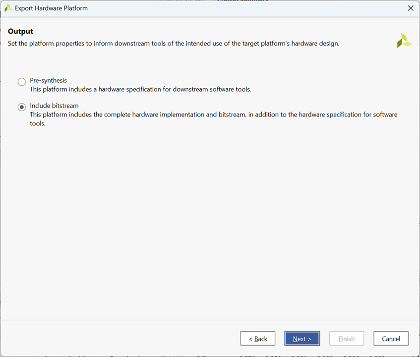
Specify a name and location for your Xilinx Shell Architecture (XSA) file.
Important: Avoid using spaces in the file name or export path. Use underscores or camelCase instead.

Review your selections and click Finish to complete the export.
Import Vitis Project
In Vitis IDE, you can effortlessly import the .zip file available for download on the Digilent reference page. The import will include the entire project, along with the Hardware platform project. Later, I will remove this project to establish a new one using the fresh .xsa file I recently created with Vivado. This new hardware platform project will then be referenced from the project intended to run on the ARM9.
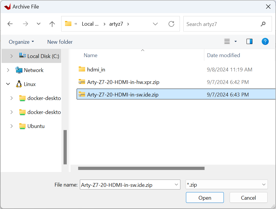
Import Vitis project
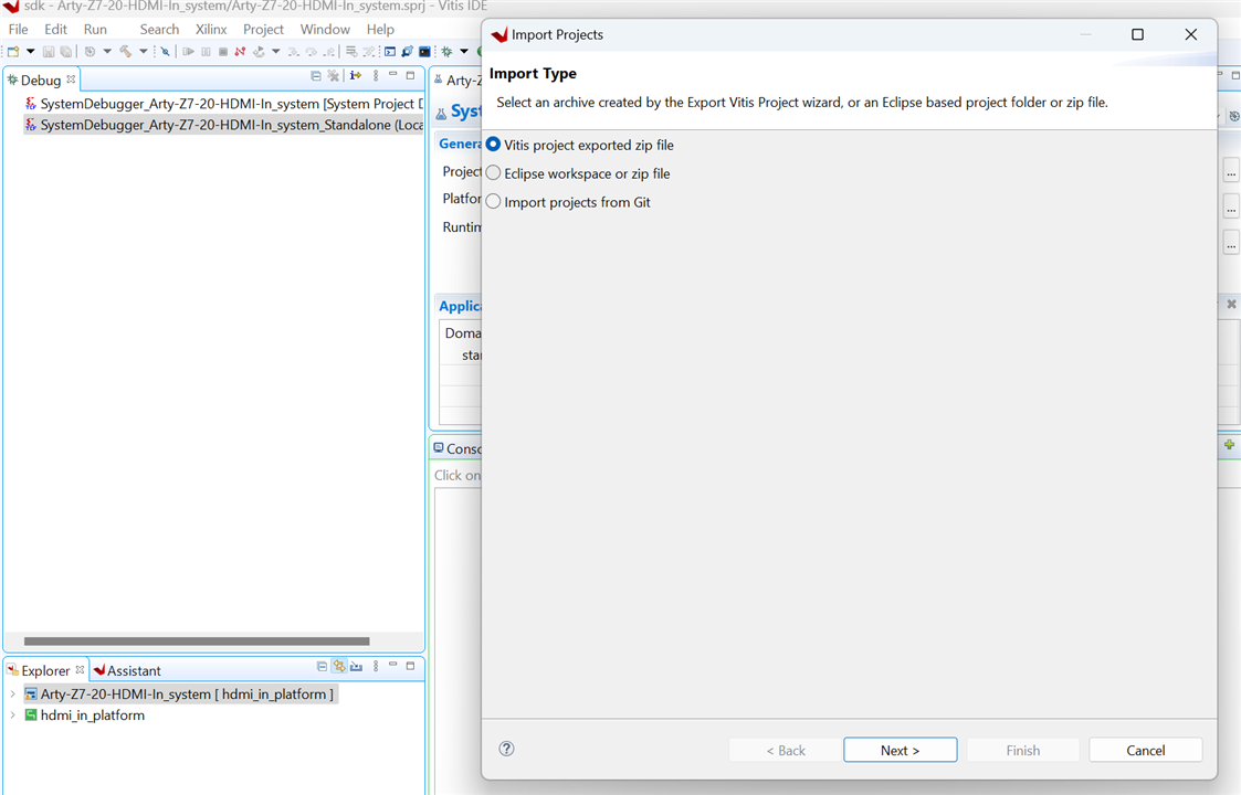
Open the software .zip file:
Platform Project Deletion: I removed the imported platform and established a new one using the exported .xsa file.

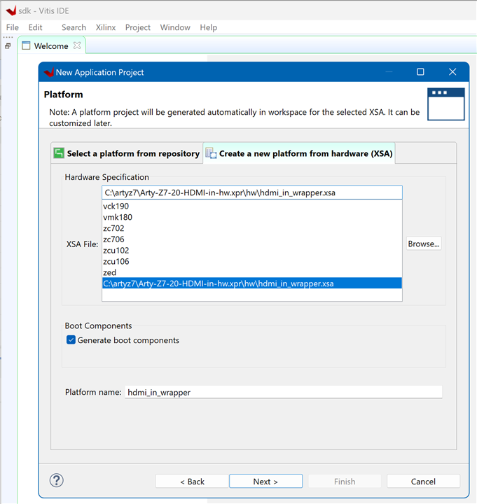
Create a new Platform Project form Hardware Specification (.xsa) using Vitis
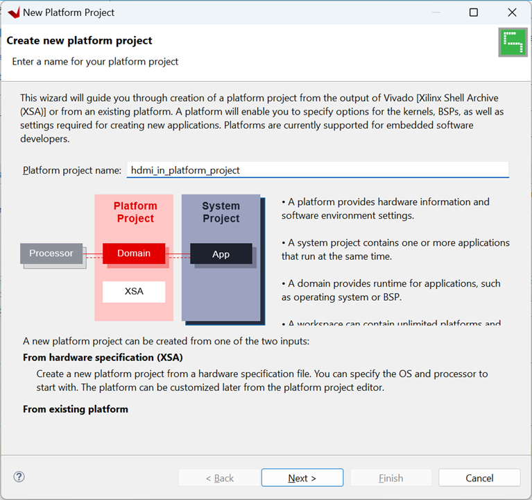
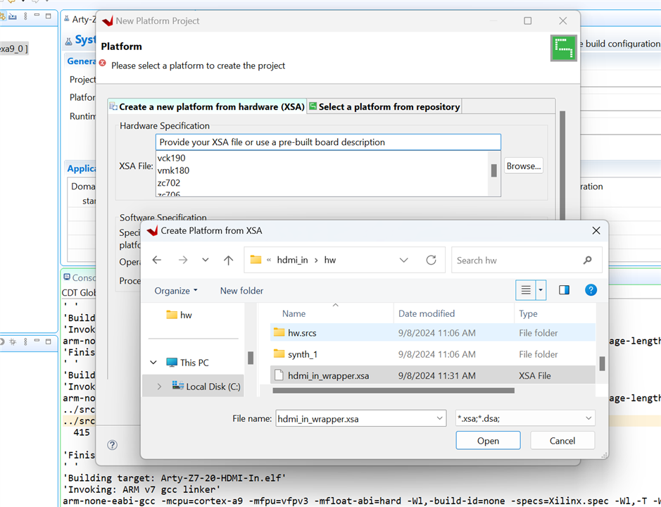
Select the newly created .xsa hardware definition file from Vivado.
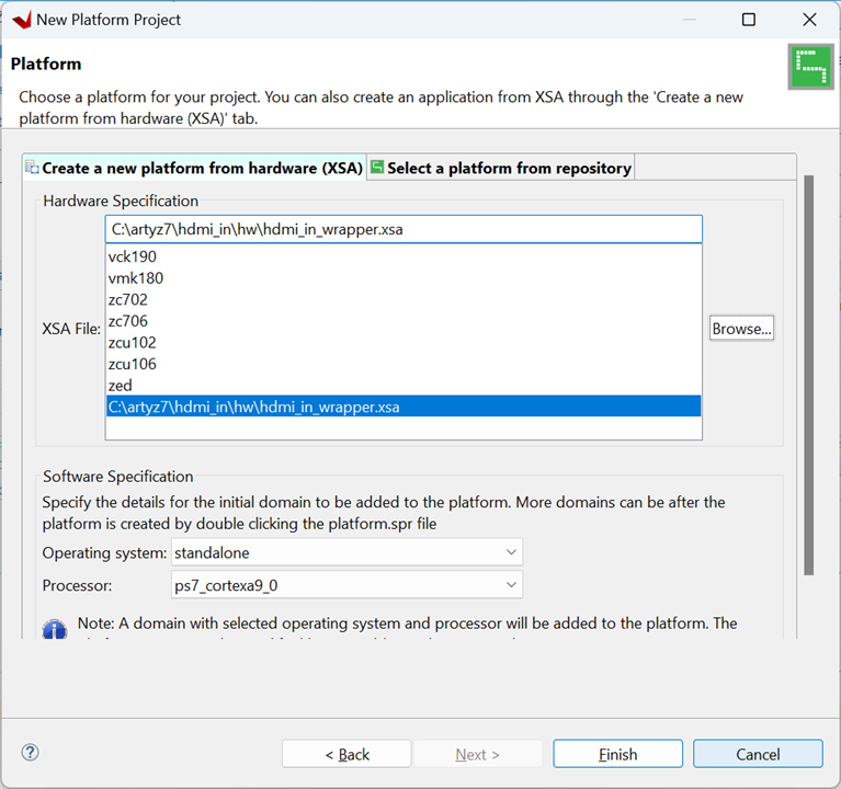
Then select the new platform for the software project:

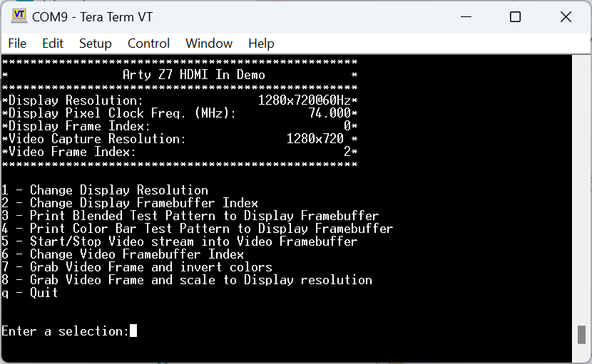
The HDMI In demo in action
I tested the demo using a Microsoft Surface Laptop as an HDMI source, with a Dockstation and a small 7" HDMI 1024x600 Color Display.
Best results were with a Display Resolution: 1280x720@60Hz
Creating a Bare Metal Boot Image
The previous example involved programming the development board using the JTAG interface, which results in the loss of configuration upon powering off the board. This section will detail how to make the programming of a project on the development board persistent. The guide outlines a step-by-step process to develop a bootloader for baremetal software applications on Zynq-7000 devices, allowing the device to boot autonomously without the need for a host computer or external connections.
Key objectives include:
- Creating a bootloader: Building a first-stage bootloader project using either Vitis.
- Generating the boot image: Combining the bootloader, bitstream, and application into a single image.
- Programming the boot image: Loading the image onto the device's storage, such as flash memory or an SD card.
- Configuring the device: Setting the board's programming mode to boot from the chosen storage.
Creating a bootloader for a previously-created baremetal software application and loading it either into SPI flash or an SD card so that it can boot without being attached to a host computer.
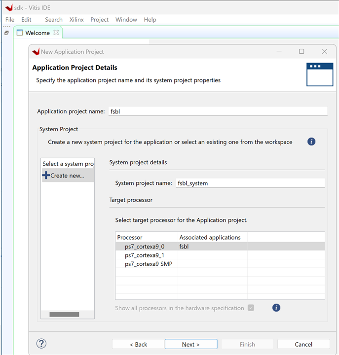
First create a first-stage bootloader project:

In Vitis, as long as the “Generate Boot Components” box was selected when the platform project was created from an XSA, the boot image will automatically be created whenever you build your system project.
Give your project a fitting name, like “fsbl”, then click “Next”.
Select a Template
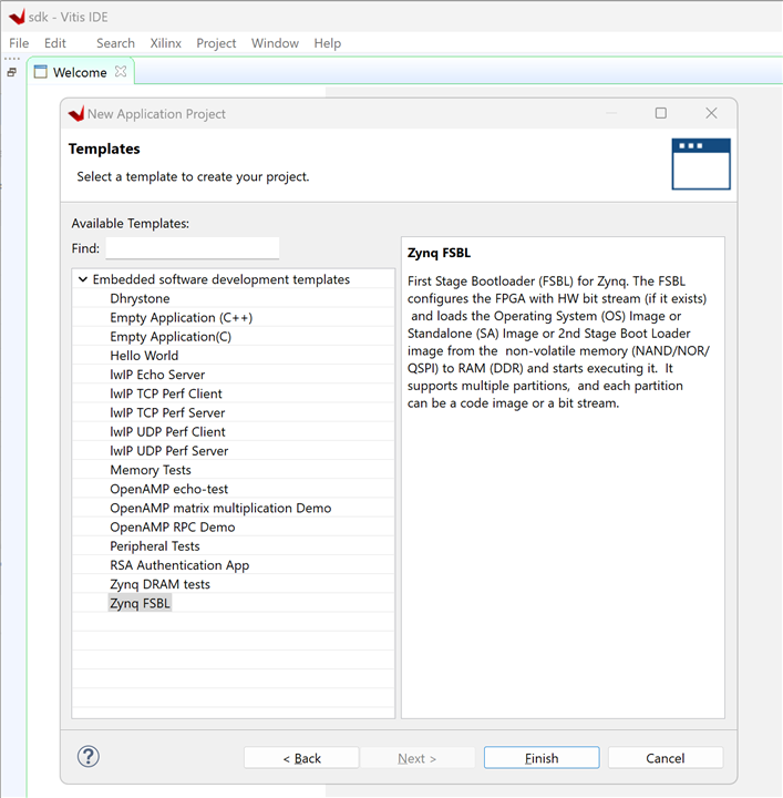
Build the project.
First, with your SDK workspace open, select the Xilinx -> Create Boot Image menu option.
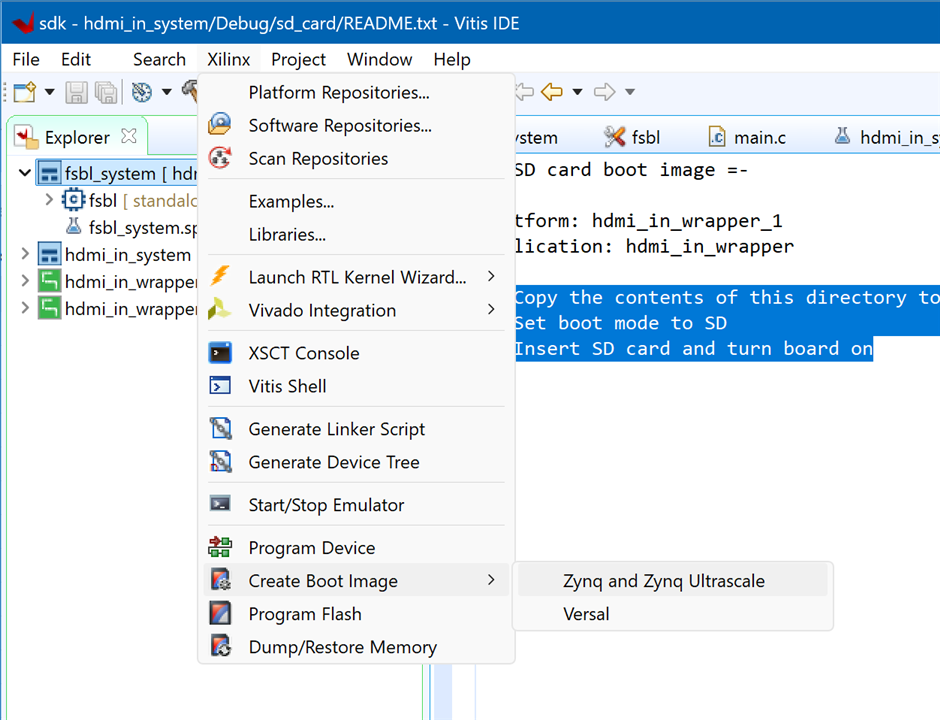

This wizard will let you define the contents of your boot image. First, select file paths where the boot image and BIF file - which stores the data entered here so that you can easily recreate the boot image when you later rebuild your project - will be written to. Then, “Add” the following three files to the image as partitions:

The FSBL ELF file, found in the FSBL project's Debug folder.
The bitstream that Vivado created for your hardware project, which can either be found in the hardware platform or in the Vivado project's .runs/impl_1 folder.
The application project's ELF file, found in the application project's Debug folder.
Once these partitions are all present, click Create Image.
cmd /C bootgen -image output.bif -arch zynq -o C:/artyz7/sdk/BOOT.bin

21:03:57 INFO : Invoking Bootgen: bootgen -image output.bif -arch zynq -o C:/artyz7/sdk/BOOT.bin
21:03:57 INFO : Creating new bif file C:\artyz7\sdk\output.bif
21:04:00 INFO : Bootgen command execution is done.


****** Xilinx Bootgen v2022.2.0
**** Build date : Oct 13 2022-12:22:51
** Copyright 1986-2022 Xilinx, Inc. All Rights Reserved.

[WARNING]: Partition fsbl.elf.0 range is overlapped with partition hdmi_in_wrapper.bit.0 memory range
[WARNING]: Partition hdmi_in_wrapper.bit.0 range is overlapped with partition hdmi_in.elf.0 memory range

[INFO] : Bootimage generated successfully
Or
Build the project. The boot image can be found in the system project's Debug folder, in the “sd_card” folder.

Flash Memory
In the menu at the top of the window, select Xilinx -> Program Flash.
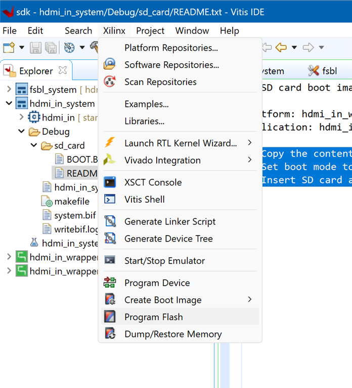
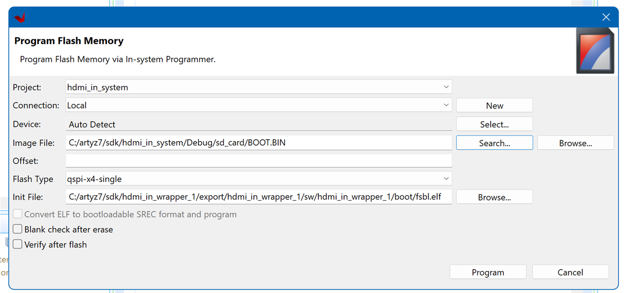
In the dialog that pops up, Browse for and select your Boot Image in the Image File field. You might want to select a specific device instead of Auto Detecting if you have multiple plugged in. You might also want to perform verification steps, available in checkboxes at the bottom of the window. No offset needs to be specified - the only thing in flash will be the image.
Once the image is in flash, all you need to do to load it is to set your board's programming mode select jumper to SPI, then power cycle it. Then copy the contents of this directory to an SD card, set boot mode to SD, insert SD card and turn board on.
You'll need a FAT32 formatted microSD card and some way to access its filesystem from your computer. Load the image into your SD card, at the root of the filesystem. The name must be “BOOT.bin”.
In order to boot from the SD card, all you need to do is slot the SD card into the board's microSD card slot, set the board's programming mode select jumper to SD, then power cycle it. The mode may have a different name, so make sure to check your board's reference manual for details.
Arty Z7 Resources
- Arty Z7 Reference Manual
- Arty Z7 Start
- Arty Z7 XDC files
- Arty Z7 Schematics
- https://github.com/Digilent/Arty-Z7-20-hdmi-out
- https://github.com/Digilent/Arty-Z7-20-hdmi-in
- https://github.com/Digilent/Arty-Z7-20-OOB
Summary
In this blog post, I introduce the FruitVisionScale project, which aims to develop a real-time embedded vision system for fruit classification and weighing. The project will employ the Digilent Arty Z7 development board, equipped with the AMD Zynq-7000 AP SoC.
The primary objectives include precise fruit classification, accurate weight measurement, system optimization, an intuitive user interface, and seamless integration with point-of-sale systems.
The post introduces the FPGA architecture and AMD tools, highlights the features of the Arty Z7, and discusses the Out-of-Box Demo. It also tackles overheating issues and illustrates the use of HDMI source and sink ports.
In subsequent blog posts, I will explore the technical aspects of the project, including the choice of machine learning algorithms, the creation of the computer vision pipeline, and the incorporation of load cells. Additionally, I will recount my experiences with the AMD tools and frameworks, along with any challenges faced during the process.
FruitVision Scale Blogs Series
- Blog 1 - FruitVision Scale - Digilent Arty Z7 - AMD Zynq-7000 - Overview
- Blog 2 - FruitVision Scale - PYNQ on the Digilent Arty Z7 - Quickstart
- Blog 3 - FruitVision Scale - Weighing strategies with load cells using the Digilent Arty Z7
- Blog 4 - FruitVision Scale - FPGA-Based HX711 Driver for Precision Weighing with AMD PYNQ
- Blog 5 - FruitVision Scale - Exploring Deep Learning Applications with AMD Zynq 7000
- Final - FruitVision Scale


