


In the previous three instalments, I covered the contents of the kit, showed you how I soldered the WL-ICLEDs and achieved “first light” using the FastLED library on the Arduino Zero and also Raspberry Pi Pico platforms. In this post, I’ll be designing actual PCBs and matching 3D printable mechanical parts that will form the main hardware deliverable of this challenge.
PCB #0: Let’s Start with Fun
With just two weeks to go, time is really running out, but so is my time to actually design and get things made-up. So, I thought it would be good to start off with something extremely simple, just so that I can say I managed to “finish” the challenge even if it wasn’t exactly what I had proposed.
From the supplied Würth Elektronik kit, I still have four types of LED to explore. For this “fun” PCB, I decided to go with the relatively tiny 1312020030000 which measures 2mm x 2mm and uses just one wire. Given I have 25 of these to play with, let’s use all of them in an “all or nothing” approach – failure is an option here.
The idea? A simple Arduino shield that would fit the Arduino Zero and host a 5x5 array of these LEDs and a simple BSS138-style level shifter. That would be sort of like a mini-size version of Würth’s IC LED Featherwing which has a 7x15 array but for an Adafruit Feather type board. I would have possibly gone with something at least seven pixels high as many fonts need at least seven pixels of height when making an LED display, but with 25 LEDs, that would mean 7 x 3 which would be very difficult to read.
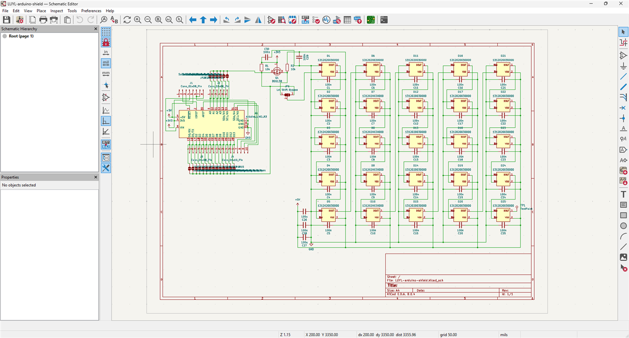
The design was relatively straightforward. I design using KiCad, so I first gathered compatible footprint, symbols and 3D models. Thankfully, Snapmagic EDA seemed to have everything I needed for the LED and the rest are just part of the standard library. As part of good practice, every LED has its own 100nF capacitor nearby to provide local decoupling, but I also provided 3 x 100uF capacitors on the board to provide more bulk capacitance as the whole array of LEDs can consume up to a total of 25 (LEDs) * 6.5 (mA/channel) * 3 (channels) = 487.5mA (total).
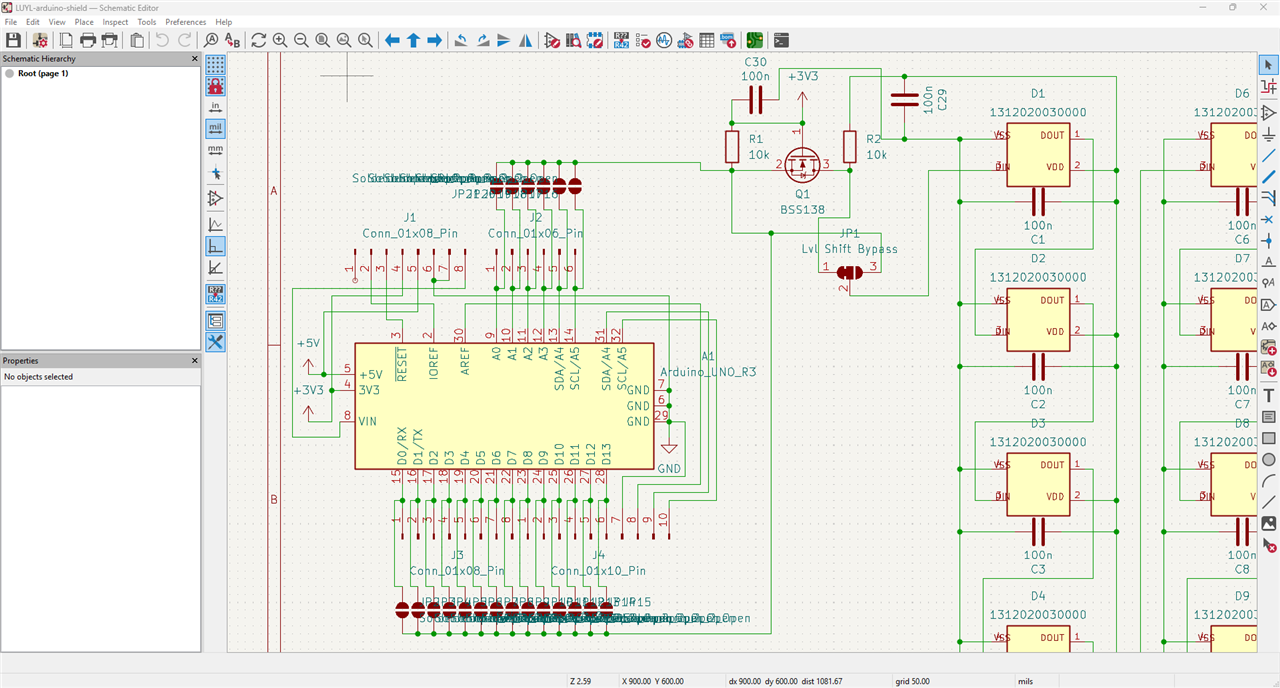
Supporting this is an Arduino Uno R3 symbol and footprint, surrogate for the Arduino Zero which shares the same form factor. To make it most convenient, I’ve added pass-through header pins so another shield could be stacked, although I don’t think you ever would want to, otherwise how would you see the LEDs? At least, that provides easier access to signal lines from the Arduino for debugging. To run the WL-ICLED chain, I’ve added a solder jumper to every I/O line to allow the user to choose any line to be the data line – maximising compatibility where other shields are used. The level shifter is unashamedly borrowed from the Sparkfun break-out I previously used – a common design used for I2C and documented by NXP. It also gets some 100nF capacitors next to it for good measure.
That’s really all there is to it – quick and simple design and one I could lay out in an evening and get sent off to the manufacturer and hopefully with enough time for economical shipping to bring it to my house for assembly.
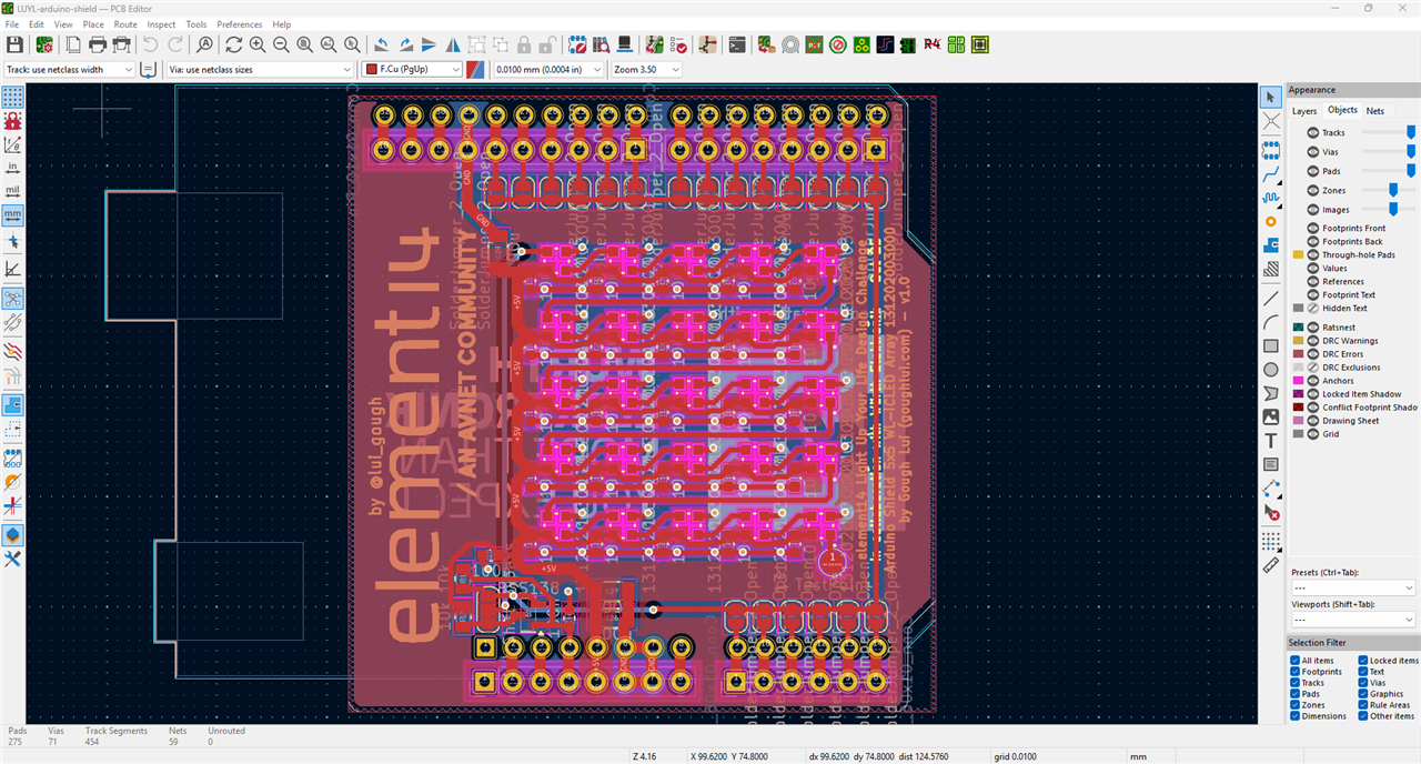
As for the layout, I opted to minimise board space to minimise costs and risk of interference with tall sockets. The top plane is used for 5V. The layout has the LEDs arranged in a matrix, with LEDs going 1234, 5678, from left to right in a “progressive” layout rather than a “serpentine” layout (which would go 1234,8765 instead).
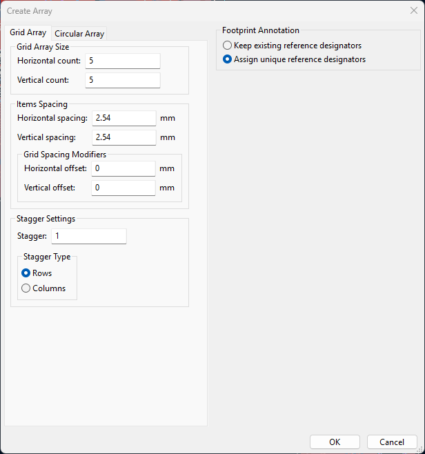
To lay this out easily, I could have used the integrated “Create Array” feature, but instead, there is an easier but slightly buggier plug-in that can do it.
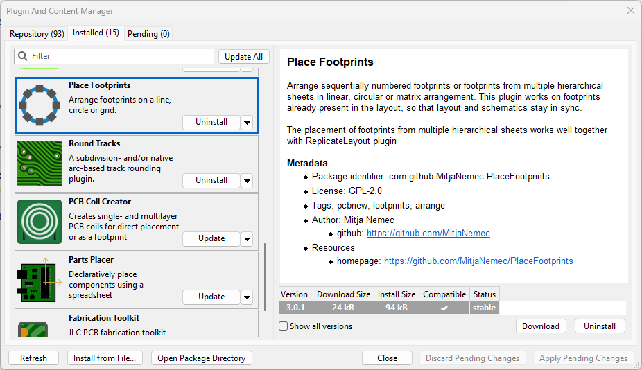
It’s called “Place Footprints” and can be installed from the Plugin and Content Manager.
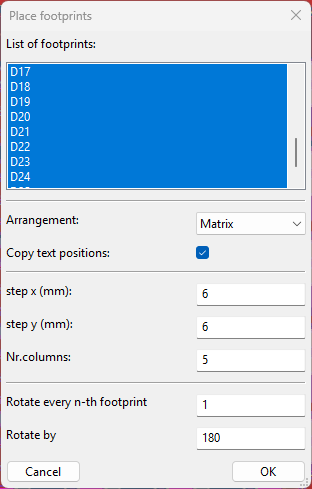
Selecting to place by designators, highlighting the designators in the list and filling in the required parameters, it automagically places everything into the right spot – all I had to do was to wire it all up together.
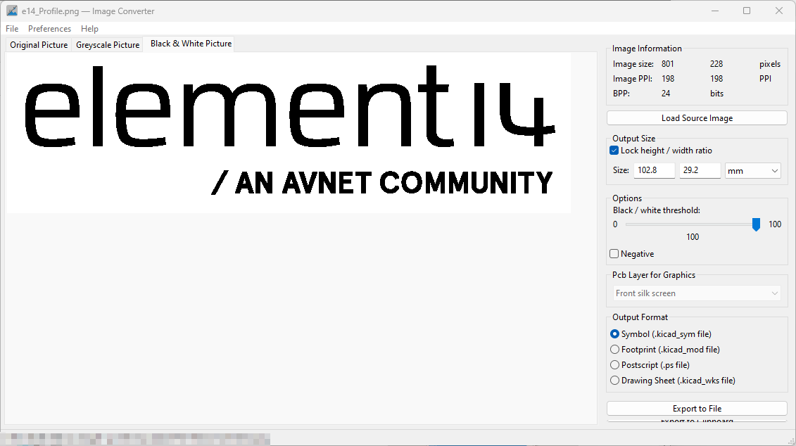
The bottom plane is used for ground with very little to interrupt it. But I wasn’t going to leave it there – I wanted it to look a little nicer, so I pinched some logos, used the Image Converter tool in KiCAD to turn them into silkscreen graphics and put them on along with some text.
After making sure the 3D models were downloaded and added into the project, I can also get a nice 3D representation of the project as a whole.

From the top, along with the element14 logo, my username and details about the challenge and the LEDs.

To the bottom, with the Würth Elektronik logo. I think it’s going to work …

Finally, a render of the LED array, looking at it at an angle. I’d say that looks good, but I’ll get the PCB made in black with white silkscreen instead, for a nicer finish. I could have changed this in the 3D rendering, but if I did, you wouldn’t see much of the traces underneath.
The project was sent to the manufacturer right away along with economical shipping option ticked as I think I should have enough time. This one isn’t the main event, but it would still be nice to have as a fallback.
For those who are interested, the Gerbers are provided here:
LUYL-Gough-Lui-arduino-shield.zip
PCB #1: The Main Event
With that out of the way, it was time to work on the real “meat” of the project, the actual lighting ring that I had proposed. This was delayed a little, owing to time taken up by work and a few other commitments, so I knew it would take some time. But it needed to be done soon – otherwise I’d have no chance of making the deadline.
For this, I first had to decide how many LEDs I would use. With 25 of each of the three remaining types at my disposal, I could throw all 25 onto the PCB, but then if I had any “accident” (say, if a chip was damaged by the heat or lost because it flew across the room in a tweezer-accident), then I would have missing LEDs. Perhaps 24 would give one spare, allowing for a 15-degree angular resolution assuming all LEDs were in-line.
But I decided to be more conservative. I reasoned that it was better to have enough spare allowance that I could experiment with soldering them comfortably, but also because of the radiation pattern of each of the LEDs were not so directional to warrant such close spacing. The edge-firing 1313210530000 and wide-area diffuse 1311610030140 has a 60-degree viewing angle to 50% intensity, while the down-firing 1312121320437 has a 55-degree viewing angle. In fact, perhaps the beamwidths are a bit wider than I had expected. You will notice that I’ve given each of the three LEDs a “role” name – that’s how I’ll be referring to them in this project.
My PCB design started with gathering footprints, symbols and 3D models for the relevant parts – again, SnapEDA came in handy as they had the data for 1313210530000, 1311610030140, 1312121320437, GCT USB4110GFA, TI TXS0108EPWR and the Raspberry Pi Pico W.
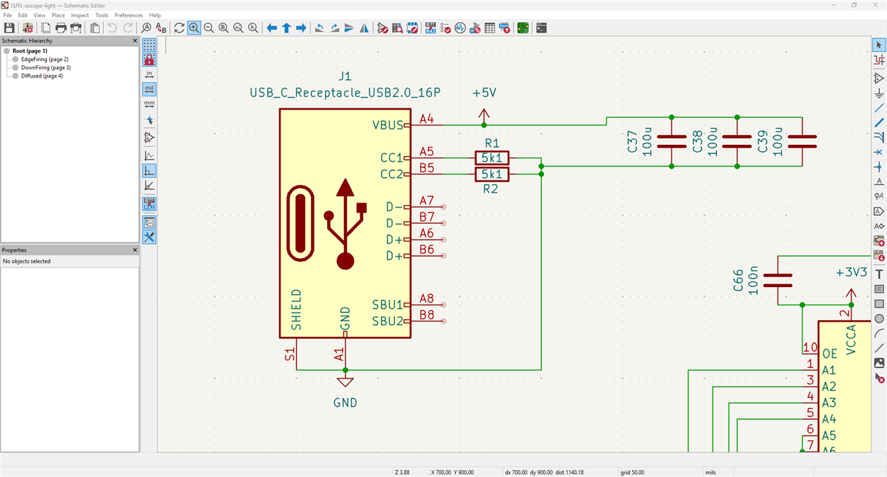
My design commenced with power, where I decided to not rely on the hateful USB micro-B of the Raspberry Pi Pico W, instead offering a USB-C connection which is much more ubiquitous nowadays. By pulling the CC lines low through 5.1k resistors, we signal to the power source that we want 5V power and depending on the power supply, we could potentially have as much as 3A. For input bypassing, another three 100uF ceramic capacitors are used.
As for how much current is actually needed in the worst-case, the math looks like this:
- 1313210530000 – 6.5mA * 3 channels * 18 LEDs = 351mA
- 1312121320437 – 23mA * 3 channels * 18 LEDs = 1,242mA
- 1311610030140 – 17.5mA (total) * 18 LEDs = 315mA
- GRAND TOTAL = 1,908mA
So, it seems a 5V/2A adapter should be about enough, but a 5V/3A USB-C adapter would be safest to provide some headroom, especially when the Wi-Fi on the Pico W is working hard. In reality, the whole point is not to be running all the LEDs at full brightness white all the time …
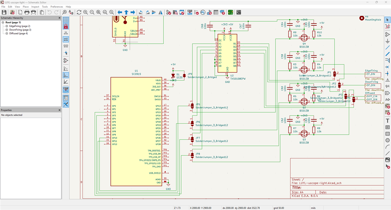
Apologies for the mess – but I do like messy schematics. It’s sort of “my thing”. Anyhow, we make use of four GPIOs to drive the three LEDs strings separately as two of them are one-wire types but with a 48-bit and a 24-bit protocol and the final one is a two-wire type. For the two-wire type, I’ve chosen GPIO 2 and 3 for hardware SPI compatibility if needed, but FastLED doesn’t seem to use it. The other two are using GPIO 10 and 11. While I do have the TXS0108EPWR level shifter hooked up and I have little doubt that it would work, I didn’t want to place all my eggs into a basket which I hadn’t tested before, so I have also broken the pins through solder jumpers to an alternative BSS138 level shifter arrangement, just in case. Who knows, perhaps if I ever needed to build another and didn’t have any of the TXS0108EPWR around, I could probably make-do with the BSS138 in a pinch. I decided to have power via a Schottky diode as an option, just in case the LED array drew too much power with a given program over the micro-USB connection. That way, plugging in micro-USB wouldn’t power the LEDs, allowing it to be programmed in peace. Alternatively, just holding BOOTSEL to invoke the ROM bootloader would work, so hence the default is to have it jumpered over. Also, off the edge of the screenshot is six M3 non-plated mounting holes – have to be able to mount this board somehow!
Here’s where the hierarchical sheets come in handy as this schematic simply wouldn’t fit onto a single page. But I use it rarely, as I like to see everything at a view.
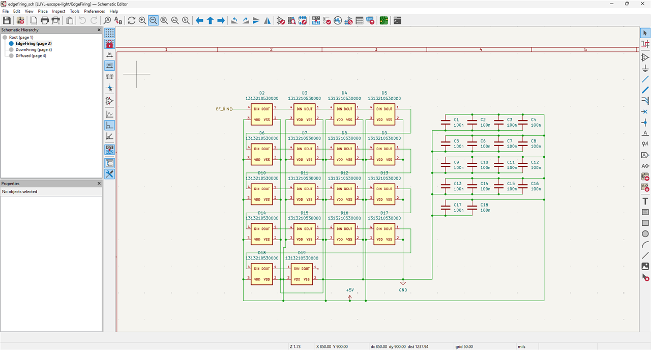
The first sheet covers the edge-firing LEDs. One LED, one capacitor, as is good form but rather than place them as such on the schematic, I just went the easy route and dumped them wherever they would fit.
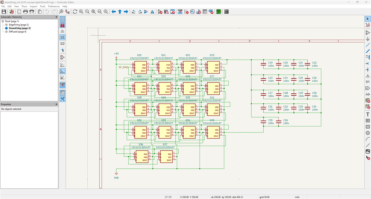
The second sheet is the down-firing LEDs. Same idea, but now with a data and bypass line to deal with. This creates a tangled wiring mess … but I still find it perfectly comprehensible. My brain’s pretty messy too …
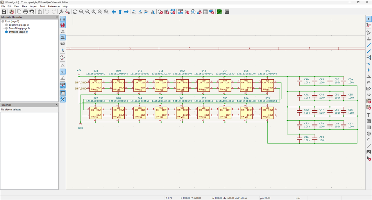
For the diffuse wide-area LEDs, I decided I had enough as the symbol had the pins in an arrangement that would make wiring absolutely a pain. So, I took the symbol and modified it – data/clock in on the left, data/clock out on the right, power from above and below. That produced this much more legible schematic.
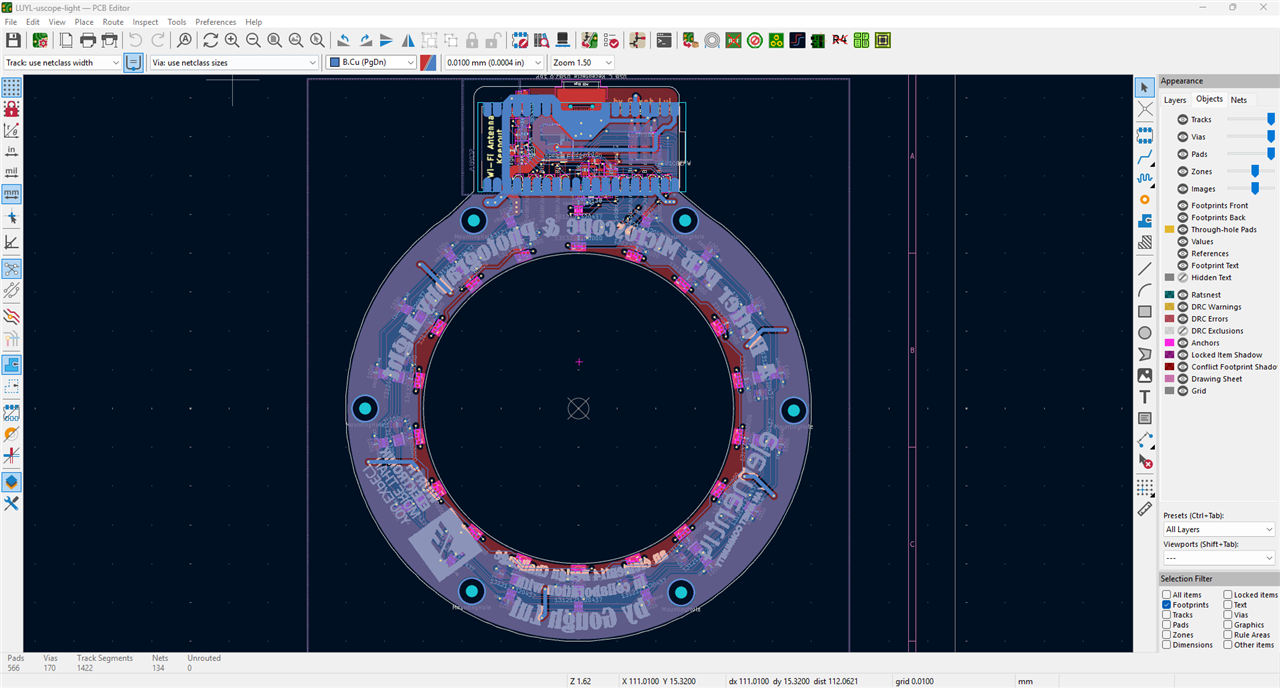
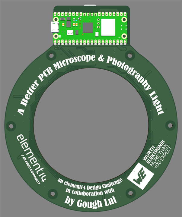
Now it was time to think of the physical dimensions and outlines of the board itself. For this, I took a measurement of my AF-S VR Micro-NIKKOR 105mm f/2.8G IF-ED lens and found it had a diameter of about 80mm, so I used this as the starting point for the hole in the centre of the PCB. As for its width – I’d like to keep the PCB as small as possible, but if it was smaller than the head of my heat-gun, there was a good chance that heat would wick around the edges, burn the PCB substrate or even the LED’s lenses. As a result, I ended up with an outer diameter of 120mm.
Even with this dimension in mind, I realised the Raspberry Pi Pico W would not “fit” in this annular ring, so I had to add a bit of a “flap” to it. In the end, that’s how we get to a layout that looks like this:
I took time to round the edges, but I eyeballed the mounting holes and got some out of place by 0.5mm. Oh well, perhaps better luck next time. Incidentally, 120mm is the same size as a CD/DVD/Blu-ray, so you can easily picture the size.
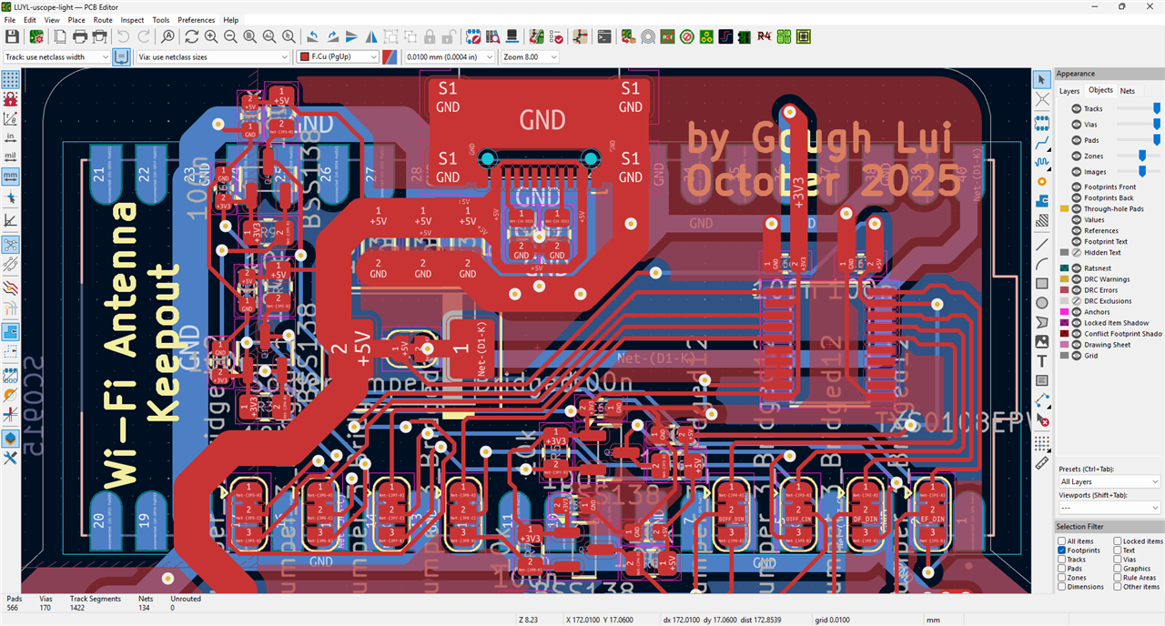
The top side of the “flap” has the level shifter arrangement and USB-C connector. It’s not the neatest but I tried to keep thick traces to keep the resistance low. I decided the top side of the board here would be ground, but then in the other part of the board, it was +5V, so that was not ideal.
The underside of the flap was reserved for the Raspberry Pi Pico W to mount, with quite a few of the unneeded pads and test-point connections removed from the footprint to avoid shorts, especially as there would be locating holes for the USB-C connector drilled into some of the unused pads. The remaining pads, even if unconnected, were left to provide mechanical support.
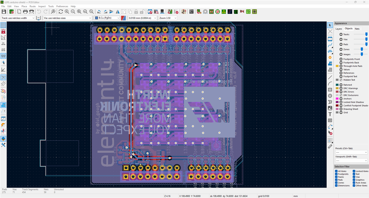
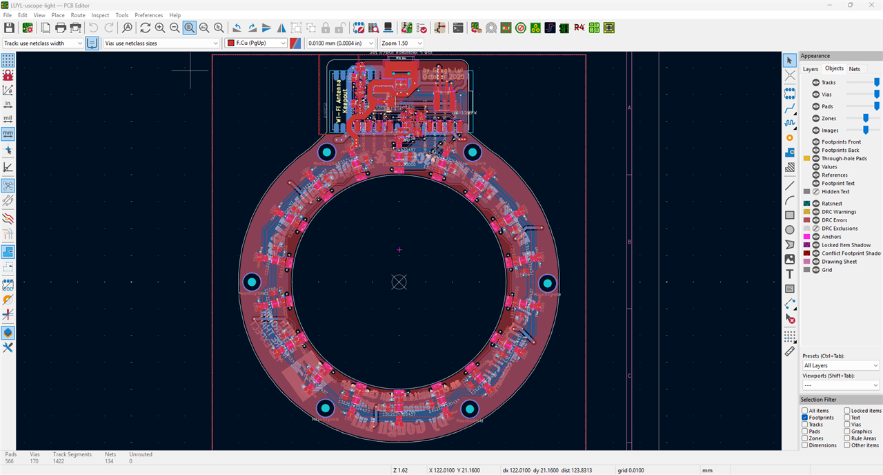
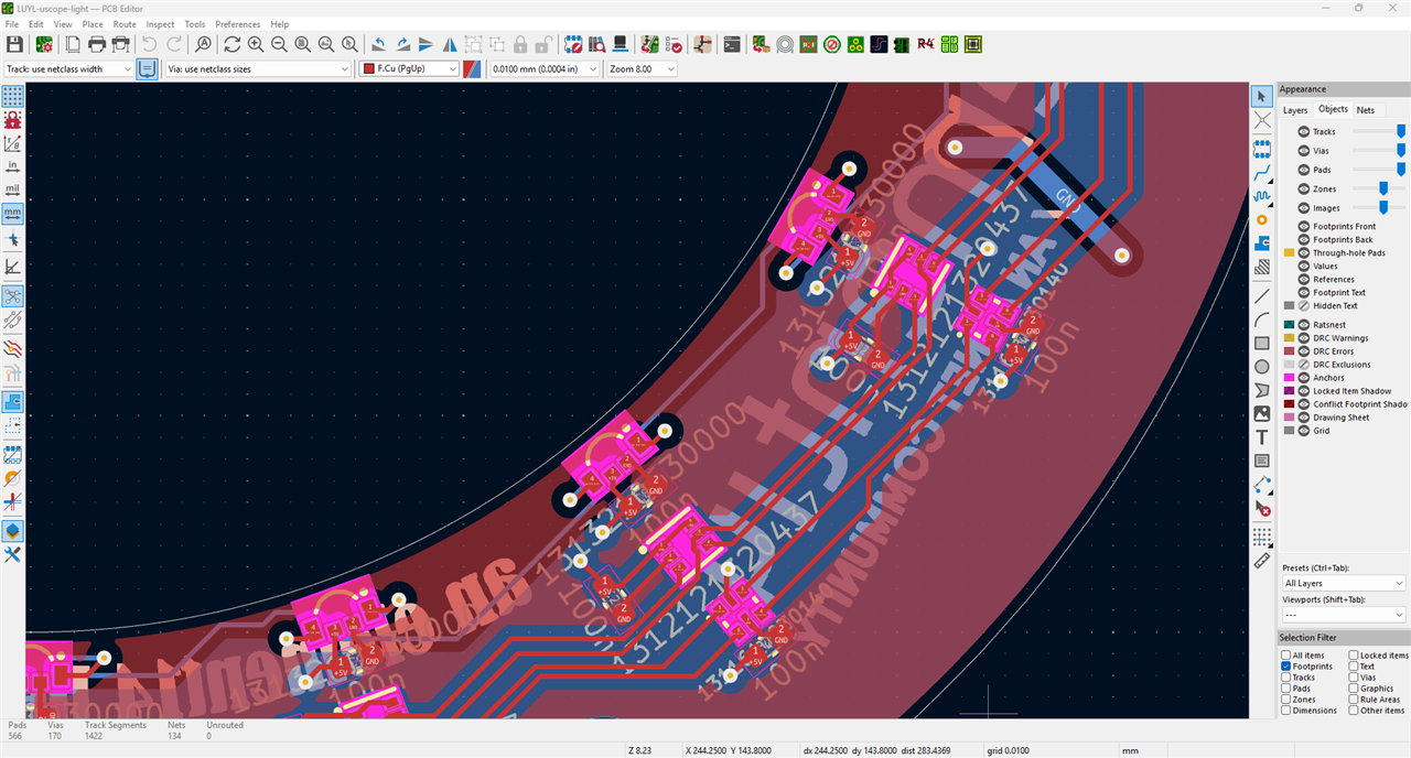
The LEDs were placed using the plugin, but this is where I noticed something interesting. It only places components clockwise around a circle, so with the edge-firing LEDs facing inwards towards the ring, the data in and data out are on the wrong side. Perhaps I could have fought and found a way to reverse this, but I decided to just let it be and patch things up with vias everywhere.
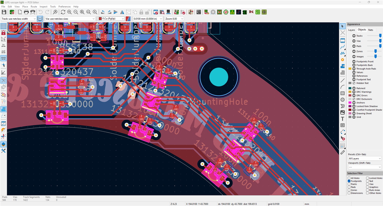
While the LEDs were in their respective places, I did have the shame of knowing that my traces were not. They were routed with the default trace settings so there are straight, 45-degree segments and vertical segments all approximating a very messy arc. I didn’t find a quick and easy way to make a trace that would go around in a nice arc – even with the curved traces plugin, it always ended up with unsmooth traces.
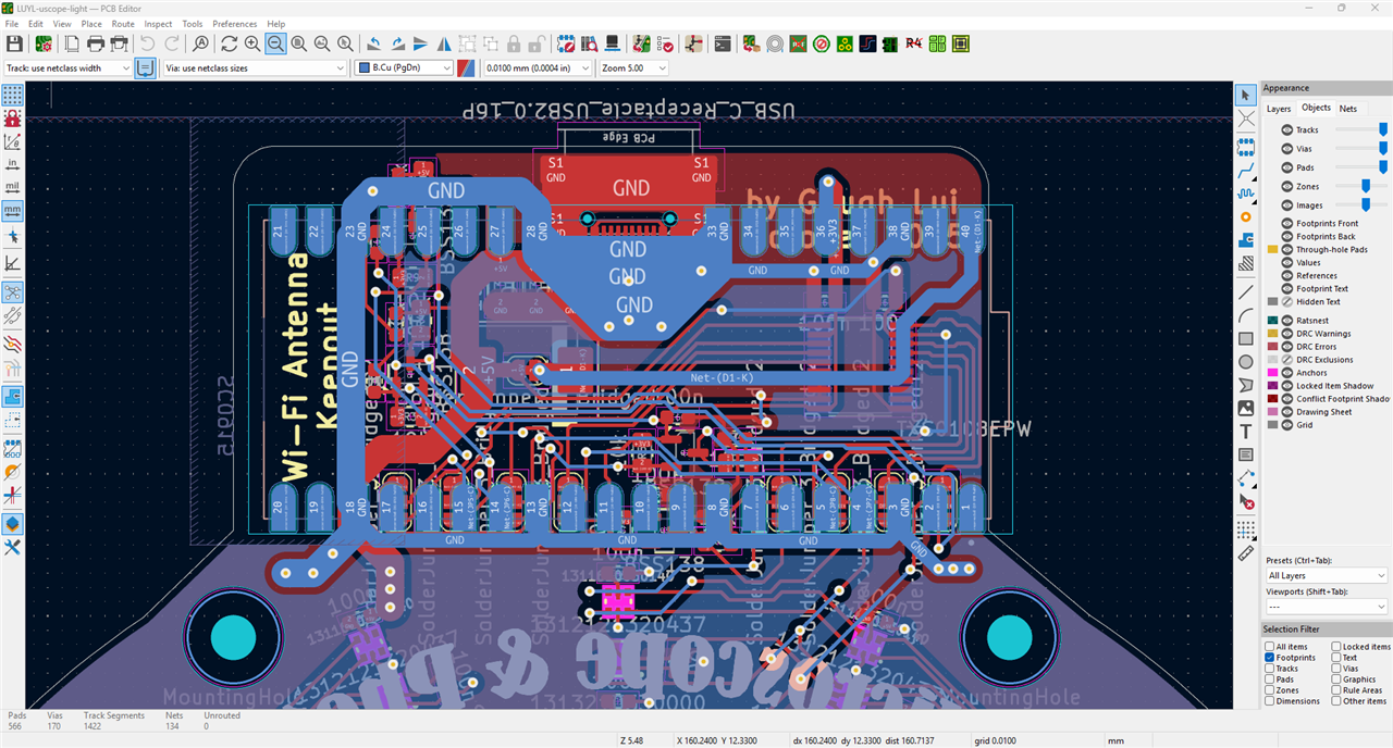
The other side has no components other than the Raspberry Pi Pico W to facilitate easier assembly, so I took advantage of that to put some silkscreen. All component designators were turned off to minimise clutter.
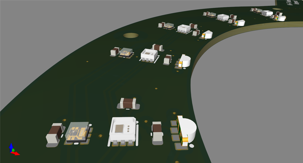
The 3D view shows the assembly more clearly, how it might look if it were constructed. Likewise, I am going to get this made in a black PCB rather than the customary green, but we can see how the LEDs are nicely and regularly spaced. Perhaps a bit of a tighter squish between the rings or running them staggered may have allowed for tighter packing, but alas, the constraint was really down to the heat gun method I intended to construct this board with.

Looking at the side view makes it clear how I intend each LED to do its job. The edge-firing LEDs will provide direct sideways illumination at a glancing angle, which might work well for chip markings. The down-firing LEDs (centre) have a much more defined radiation pattern, so should control their angle quite well. The diffused wide-angle LEDs have a less defined radiation pattern, so would provide more “even” lighting, or add supplemental “fill” light in case the others are not sufficiently bright.
Taking a little more time, I got fancy with Photoshop for the silkscreen artwork, making this wonderful design for the rear of the board (with “borrowed” logos). What a shame that, once assembled (in the way I envisioned) that most of this won’t be visible at all.
The Gerbers for this PCB design were sent off to the manufacturer as soon as they were done – this time, as it took several days to get it together in my spare time, I ended up shelling out for DHL Express courier. If you’re interested, the PCB Gerbers can be downloaded here:
LUYL-Gough-Lui-uscope-light.zip
A Mechanical Design for 3D Printing
Even if I have a nice multi-ring RGB LED array, it’s not particularly fit-for-purpose unless it can be mounted in front of a camera lens or a digital microscope. As a result, I needed to design a carrier that would mount, on one side, to the PCB and on the other, to the lens or assembly. I decided that this would be best designed in two parts – the first part would be the part that held the PCB and adapted it to a flat surface. Then, the second part would adapt the lens to a flat surface where both could be joined together. This way the design would be 3D printable without the need for much in the way of support or risky overhangs. After all, my 3D printers are getting a bit long in the tooth being a Anycubic Mega Pro based around Marlin firmware (suffering from worn extruders, occasional hot-end jams, bed warpage/adhesion difficulties and sloppy belts).
As I’m not particularly skilled when it comes to 3D CAD design, I used the only tool I knew how to use – Autodesk Tinkercad, a web-browser-based basic CAD tool that is targeted predominantly at the education market.
After extracting the hole co-ordinates of the PCB from KiCAD, I used the ruler in Tinkercad and placed the necessary holes to match. Then, by using a mixture of cylindrical holes, rectangular holes and filled rings, I had a design that looked like this:

This protection ring would accept the PCB from its front, having a lip several millimeters high such that resting the ring on the bench will not result in any damage. This is necessary since the bare PCB has the LEDs projecting from it – especially the edge-mounted ones, which would be begging to get knocked off.

A cut-out is made at the top to allow for the height protrusion of the Raspberry Pi Pico W and associated ports – no attempt is made to protect those by enclosing them – it would have complicated the design significantly to do that. But it is also seen that there is about 6mm of material behind the back of the PCB and the bottom of the plate – this is the depth to allow for screws to “bite” into the plastic. I made 2.85mm diameter holes to accept M3 screws without the need for nuts – this isn’t suitable for high-torque fixing but for simple light-weight stuff like this, it would be strong enough.
I also added an additional constellation of holes – five in total, that would be used by the other adapter plate, two of which roughly overlap with the PCB holes.
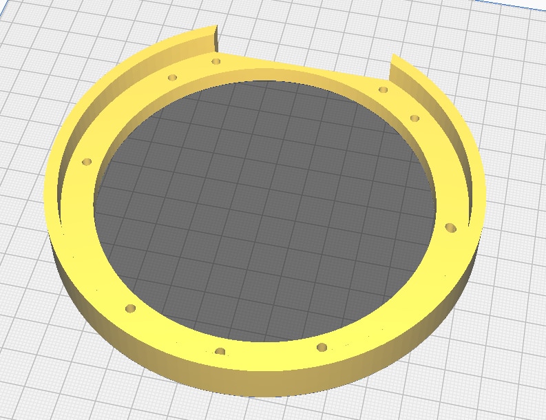
The STL when exported and imported into Ultimaker Cura (to slice for the 3D printer) looks as above – making it clear how the model looks.
The second part that needed to be designed was the adapter ring that would connect to the lens and secure that to the protection ring.

I decided to draw a somewhat convoluted design involving rectangular 3mm thick “arms” that would reach out to each of the anchor points, trimmed by an annular “hole” to have a nice rounded outer edge.

The inside would accommodate the lens’ 80mm diameter exactly, with a bit of a thick wall such that it can accept three longer M3 screws to secure the ring to a smaller-diameter neck – for example, on a digital microscope. It’s not a damage-free way to do it, but it would be the simplest.
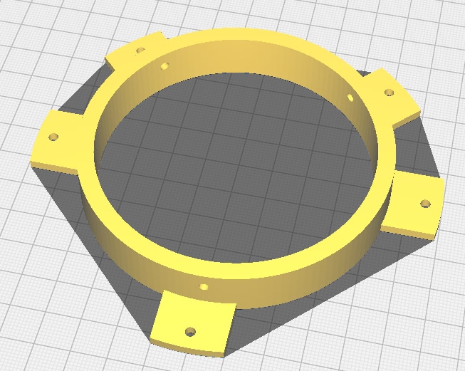
The design as seen in Cura is most easiest to understand – but those five anchor points will be screwed into the protection ring when both flat-sides are aligned with each other, using M3 screws. It should provide sufficient strength to hold the assembly together even in the case of slight bumps and with the residual torque of a USB-C power cable.
Finally, is the design for a diffuser cover – which means thin sections of ideally translucent clear plastic. To do this, I had to get creative with the tools in Tinkercad, but I managed.

A mixture of solid cylinder, cylindrical hole and annular hole managed to create the “round flat-bottomed U-channel” that I desired.
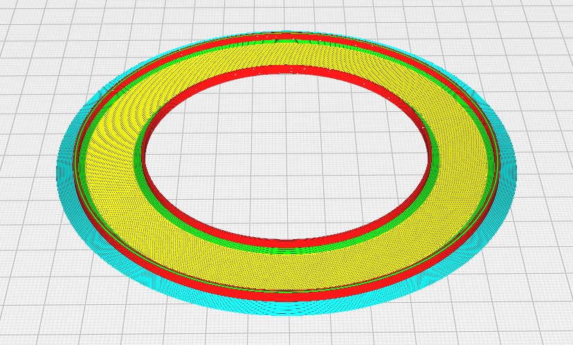
Viewing the print simulation in Cura, it’s clear just how thin the inner wall is, as I didn’t want to interfere too much with the edge-firing LEDs while also wanting to collect any spill-over from the other rows of LEDs. The bottom itself is three layers thick – hopefully not too thick as to cause a significant loss of light.
For those who are interested in the 3D printing files, I will caution that these are untested preliminary prototype designs, so use at your own risk, but the STLs can be downloaded here:
One potential change might be that I might want to create a diffuser that has baffles instead – radial partitions printed with dark plastic (multi-material print through pausing and swapping materials) so as to segment the arc into separate “pockets” to increase the angular resolution of the light. But to design this in Tinkercad will take quite a bit of time … so for now, let’s just see how well the current design works first.
Conclusion
In all, the PCB designs are relatively straightforward even if they’re slightly rough in some ways – I wish I knew how to make nice arc traces easily in KiCAD but alas, what is done should still work (in theory). Likewise, the 3D mechanical designs are definitely rough, as I’m very much a novice when it comes to CAD and I’m using a relatively crude tool to design with, but it should still create something that allows for the solution to mount onto the front of a macro lens or potentially a digital microscope with the option of a light diffuser (assuming you have access to the right sort of translucent plastic).
Now, it’s time to wait (patiently) for the PCBs to arrive and for the 3D printer to finish “chugging” away at the 3D prints to see if this project will come together in terms of its hardware. But in the meantime, I thought it would be fun to run a couple of polls – no prizes for getting the correct answer, but feel free to take a guess and leave a comment about why you voted in any particular way.


