


Here are the previous blogs in this series:
Prototyping with FPGAs - Part 1 - Basics
Prototyping with FPGAs - Part 2 - Combinational Logic with Xilinx ISE on Spartan 6 FPGA
Prototyping with FPGAs - Part 3 - Sequential Logic with Quartus Prime on Cyclone-IV FPGA

Aim: To compare and analyze the performance of Shifters using Combinational Logic and Sequential Logic implemented on Artix-7 FPGA
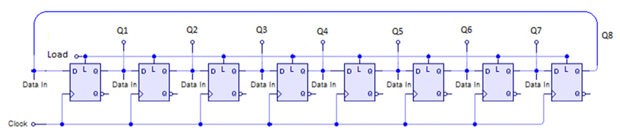
Sequential Logic: The Shift Registers
We all know what shift registers are, and why they are used - to shift bits in a register right?
But the applications inside a CPU or Microcontroller are vast and play a crucial role in Arithmetic and Logic Units especially in ARM Processors these days.
The design given below is specific to shift right. But why? This operation was used in the vintage 8086 microprocessor to implement the ROR instruction.
8-bit Shift Registers Design:

Verilog Implementation:

Is there any other way to shift the bits?
- Yes, the barrel shifter.
Combinational Logic: The Barrel Shifter

Truth Table:

In this blog, I'm going to discuss the design and implementation of 8-bit barrel shifters using Multiplexers.
The modeling I'm going to follow is Structural design in Verilog HDL.
First of all, to get started let's design a 2:1 Mux
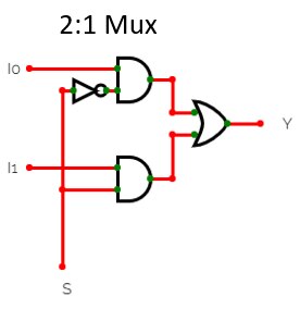

Verilog code for the 2:1 Mux in structural model is pretty simple, we have 2 AND Gates, 1 NOT Gate, and 1 OR Gate.
Apart from regular inputs and outputs, three wires are declared for the gate outputs and are connected according to the structure.
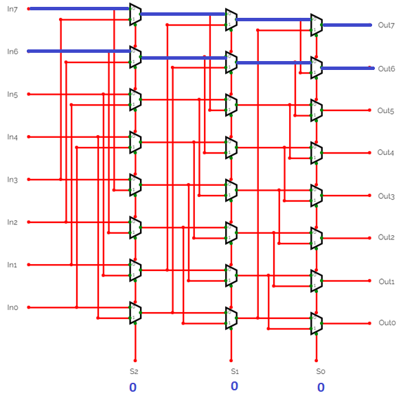
Design of 8-bit Barrel Shifter:
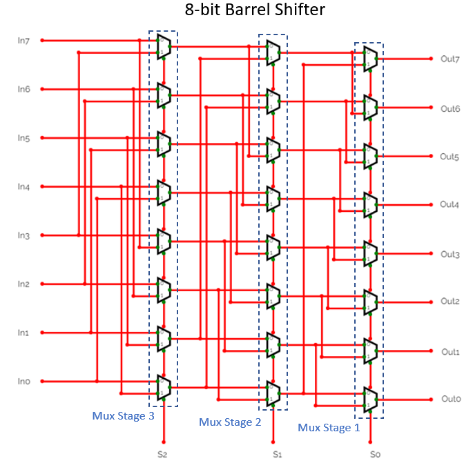
By using the structural design, we can make sure the design is implemented in the way we want it to be.
Verilog Implementation:

Working of Barrel Shifter :
| {gallery} BS |
|---|
No Shift |
Shift by 1 bit (001) |
Shift by 2 bits (010) |
Shift by 4 bits (100) |
Shift by 3 bits (011) |
Shift by 7 bits (111) |


This is how the barrel shifter shifts the bits according to the select lines.

Implementation on Artix-7 FPGA:
I will be using the USB104-A7 FPGA Development Board for the implementation. This was road-tested a few months back. Read the review here: USB104 A7: Artix-7 FPGA Development Board - Review

Fabrication of custom Pmod:
A custom Pmod (Peripheral Module) was to be fabricated for implementing digital designs as there was very few user I/O peripherals such as push buttons and LEDs.
Let's take a look at the schematic for the fabrication.


Design made with NI Multisim:
From the schematics, it can be understood that using a 10k resistor would be used for pull-up and pull-down purposes.
As there is already a 200 Ohm resistor connected in series to the Pmod GPIO to prevent damage to the FPGA if one accidentally drives an input as an output,
only 100 Ohm resistor is used in series with the LEDs. All switches are active high. The circuit diagram is given below:


Started with the above components, some PCB mount slide switches, LEDs, and the Bent Male-Male Dual pin headers.
After soldering all the components and the connections:
Front - end Back-end

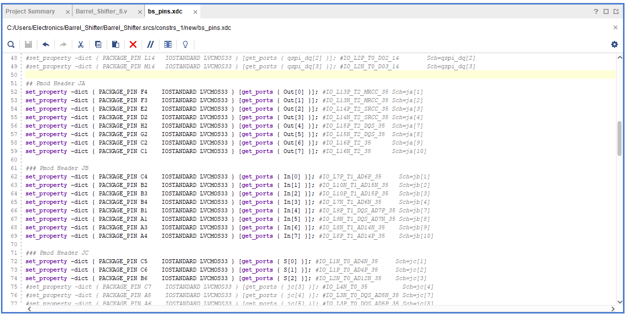
Here is the general constraints file for the above-fabricated Pmod:
## Pmod Header JA
#set_property -dict { PACKAGE_PIN F4    IOSTANDARD LVCMOS33 } [get_ports { led[0] }]; #IO_L13P_T2_MRCC_35 Sch=ja[1]
#set_property -dict { PACKAGE_PIN F3    IOSTANDARD LVCMOS33 } [get_ports { led[1] }]; #IO_L13N_T2_MRCC_35 Sch=ja[2]
#set_property -dict { PACKAGE_PIN E2    IOSTANDARD LVCMOS33 } [get_ports { led[2] }]; #IO_L14P_T2_SRCC_35 Sch=ja[3]
#set_property -dict { PACKAGE_PIN D2    IOSTANDARD LVCMOS33 } [get_ports { led[3] }]; #IO_L14N_T2_SRCC_35 Sch=ja[4]
#set_property -dict { PACKAGE_PIN H2    IOSTANDARD LVCMOS33 } [get_ports { led[4] }]; #IO_L15P_T2_DQS_35  Sch=ja[7]
#set_property -dict { PACKAGE_PIN G2    IOSTANDARD LVCMOS33 } [get_ports { led[5] }]; #IO_L15N_T2_DQS_35  Sch=ja[8]
#set_property -dict { PACKAGE_PIN C2    IOSTANDARD LVCMOS33 } [get_ports { led[6] }]; #IO_L16P_T2_35      Sch=ja[9]
#set_property -dict { PACKAGE_PIN C1    IOSTANDARD LVCMOS33 } [get_ports { led[7] }]; #IO_L16N_T2_35      Sch=ja[10]
### Pmod Header JB
#set_property -dict { PACKAGE_PIN C4    IOSTANDARD LVCMOS33 } [get_ports { sw_b[0] }]; #IO_L7P_T1_AD6P_35     Sch=jb[1]
#set_property -dict { PACKAGE_PIN B2    IOSTANDARD LVCMOS33 } [get_ports { sw_b[1] }]; #IO_L10N_T1_AD15N_35   Sch=jb[2]
#set_property -dict { PACKAGE_PIN B3    IOSTANDARD LVCMOS33 } [get_ports { sw_b[2] }]; #IO_L10P_T1_AD15P_35   Sch=jb[3]
#set_property -dict { PACKAGE_PIN B4    IOSTANDARD LVCMOS33 } [get_ports { sw_b[3] }]; #IO_L7N_T1_AD6N_35     Sch=jb[4]
#set_property -dict { PACKAGE_PIN B1    IOSTANDARD LVCMOS33 } [get_ports { sw_b[4] }]; #IO_L9P_T1_DQS_AD7P_35 Sch=jb[7]
#set_property -dict { PACKAGE_PIN A1    IOSTANDARD LVCMOS33 } [get_ports { sw_b[5] }]; #IO_L9N_T1_DQS_AD7N_35 Sch=jb[8]
#set_property -dict { PACKAGE_PIN A3    IOSTANDARD LVCMOS33 } [get_ports { sw_b[6] }]; #IO_L8N_T1_AD14N_35    Sch=jb[9]
#set_property -dict { PACKAGE_PIN A4    IOSTANDARD LVCMOS33 } [get_ports { sw_b[7] }]; #IO_L8P_T1_AD14P_35    Sch=jb[10]
### Pmod Header JC
#set_property -dict { PACKAGE_PIN C5    IOSTANDARD LVCMOS33 } [get_ports { sw_a[0] }]; #IO_L1N_T0_AD4N_35     Sch=jc[1]
#set_property -dict { PACKAGE_PIN C6    IOSTANDARD LVCMOS33 } [get_ports { sw_a[1] }]; #IO_L1P_T0_AD4P_35     Sch=jc[2]
#set_property -dict { PACKAGE_PIN B6    IOSTANDARD LVCMOS33 } [get_ports { sw_a[2] }]; #IO_L2N_T0_AD12N_35    Sch=jc[3]
#set_property -dict { PACKAGE_PIN C7    IOSTANDARD LVCMOS33 } [get_ports { sw_a[3] }]; #IO_L4N_T0_35          Sch=jc[4]
#set_property -dict { PACKAGE_PIN A5    IOSTANDARD LVCMOS33 } [get_ports { sw_a[4] }]; #IO_L3N_T0_DQS_AD5N_35 Sch=jc[7]
#set_property -dict { PACKAGE_PIN A6    IOSTANDARD LVCMOS33 } [get_ports { sw_a[5] }]; #IO_L3P_T0_DQS_AD5P_35 Sch=jc[8]
#set_property -dict { PACKAGE_PIN B7    IOSTANDARD LVCMOS33 } [get_ports { sw_a[6] }]; #IO_L2P_T0_AD12P_35    Sch=jc[9]
#set_property -dict { PACKAGE_PIN D8    IOSTANDARD LVCMOS33 } [get_ports { sw_a[7] }]; #IO_L4P_T0_35          Sch=jc[10]
Getting Started with Vivado:
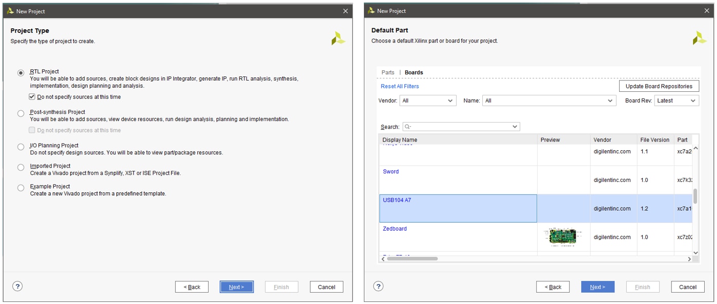
| {gallery} Vivado |
|---|
Create new project |
Give the project a name without spaces |
Choose the board |
Finish |
Click on add new sources |
|
Select the files required |
You will see the instances on the left panel |
Add the constraints file |
|
Give the exact constraints name |
Regular Design flow |
|
|


Make sure to add a command in the constraints file of the shift register project if you're planning to use the push button on the FPGA board as the implementation won't complete due to a clock dedicated route error.

8-bit Shift Register on Artix-7 FPGA:
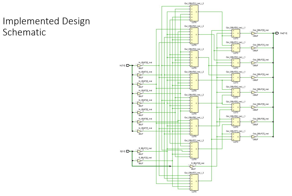
8-bit Barrel Shifter on Artix-7 FPGA:
Final Comparison after implementation:

Thanks for Reading!