element14 Community
element14 Community
    Register Log In
  • Site
  • Search
  • Log In Register
  • About Us
  • Community Hub
    Community Hub
    • What's New on element14
    • Feedback and Support
    • Benefits of Membership
    • Personal Blogs
    • Members Area
    • Achievement Levels
  • Learn
    Learn
    • Ask an Expert
    • eBooks
    • element14 presents
    • Learning Center
    • Tech Spotlight
    • STEM Academy
    • Webinars, Training and Events
    • Learning Groups
  • Technologies
    Technologies
    • 3D Printing
    • FPGA
    • Industrial Automation
    • Internet of Things
    • Power & Energy
    • Sensors
    • Technology Groups
  • Challenges & Projects
    Challenges & Projects
    • Design Challenges
    • element14 presents Projects
    • Project14
    • Arduino Projects
    • Raspberry Pi Projects
    • Project Groups
  • Products
    Products
    • Arduino
    • Avnet Boards Community
    • Dev Tools
    • Manufacturers
    • Multicomp Pro
    • Product Groups
    • Raspberry Pi
    • RoadTests & Reviews
  • Store
    Store
    • Visit Your Store
    • Choose another store...
      • Europe
      •  Austria (German)
      •  Belgium (Dutch, French)
      •  Bulgaria (Bulgarian)
      •  Czech Republic (Czech)
      •  Denmark (Danish)
      •  Estonia (Estonian)
      •  Finland (Finnish)
      •  France (French)
      •  Germany (German)
      •  Hungary (Hungarian)
      •  Ireland
      •  Israel
      •  Italy (Italian)
      •  Latvia (Latvian)
      •  
      •  Lithuania (Lithuanian)
      •  Netherlands (Dutch)
      •  Norway (Norwegian)
      •  Poland (Polish)
      •  Portugal (Portuguese)
      •  Romania (Romanian)
      •  Russia (Russian)
      •  Slovakia (Slovak)
      •  Slovenia (Slovenian)
      •  Spain (Spanish)
      •  Sweden (Swedish)
      •  Switzerland(German, French)
      •  Turkey (Turkish)
      •  United Kingdom
      • Asia Pacific
      •  Australia
      •  China
      •  Hong Kong
      •  India
      •  Korea (Korean)
      •  Malaysia
      •  New Zealand
      •  Philippines
      •  Singapore
      •  Taiwan
      •  Thailand (Thai)
      • Americas
      •  Brazil (Portuguese)
      •  Canada
      •  Mexico (Spanish)
      •  United States
      Can't find the country/region you're looking for? Visit our export site or find a local distributor.
  • Translate
  • Profile
  • Settings
Personal Blogs
  • Community Hub
  • More
Personal Blogs
Legacy Personal Blogs Hercules LaunchPad and GaN FETs - Part 2: Make a BoosterPack
  • Blog
  • Documents
  • Mentions
  • Sub-Groups
  • Tags
  • More
  • Cancel
  • New
  • Share
  • More
  • Cancel
Group Actions
  • Group RSS
  • More
  • Cancel
Engagement
  • Author Author: Jan Cumps
  • Date Created: 12 Sep 2016 11:55 AM Date Created
  • Views 3398 views
  • Likes 11 likes
  • Comments 19 comments
  • gallium_nitride
  • smart_instrument
  • boosterpack
  • lmg5200
  • texas_instruments
  • labview
  • gan
  • hercules
  • launchpad
  • test_automation
Related
Recommended

Hercules LaunchPad and GaN FETs - Part 2: Make a BoosterPack

Jan Cumps
Jan Cumps
12 Sep 2016

I'm designing a BoosterPack to evaluate GaN devices with the help of a microcontroller.


             image


The kit will have a GaN half-bridge that can control an output of 20V and 10A.

Currently the prototype can control switching frequency and duty cycle.

I'm also planning a stretch goal to integrate the design with LabView. You can then use this as a part of a test setup.


The Design Exists


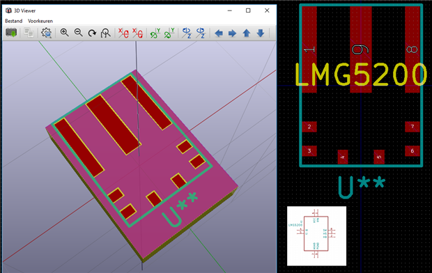
I have a working prototype. I modded an existing LMG5200 evaluation kit a while ago.

I removed the discrete PWM generator and replaced it with microcontroller managed signals.

image


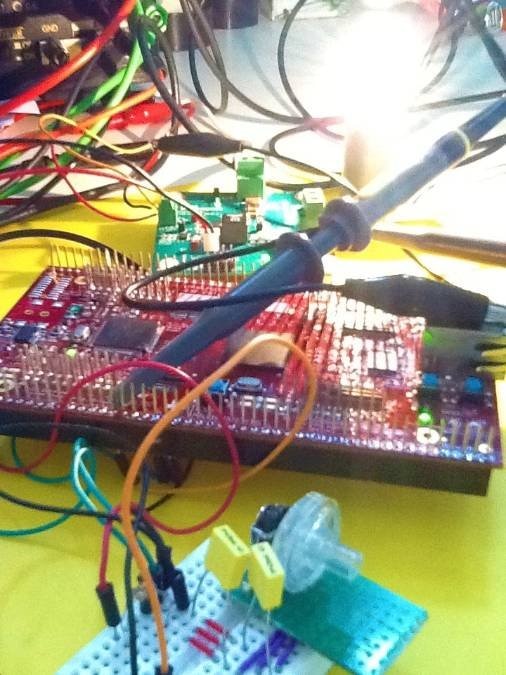
This proof of concept works, both electronics and firmware. I can make a more sturdy version now.

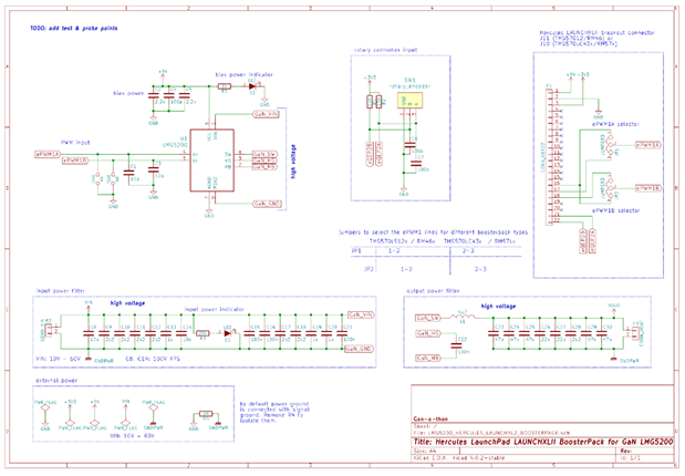
The switching layout is fully based on the design guidelines and the evaluation kit's PCB.

Because of the high switching frequencies and high currents, that part of the design is critical.

I'm trying to place all components similar to the application notes. This will be my first 4-layer PCB design.


Status


I have the schematic ready.

I had to create a few components and footprints (both for LMG5200 and rotary encoder, footprint only for the inductor).

image

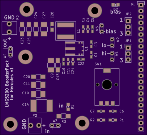
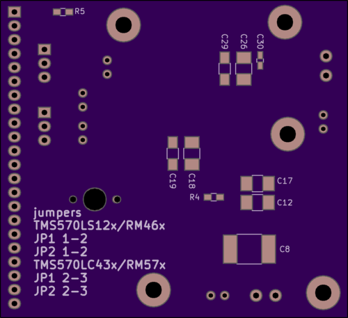
For the PCB, I have a provisional layout. I haven't routed a single trace yet.

But I have uploaded that intermediate status to OSHPark to get an idea of how this device will look like.

Before doing that routing, I first have to verify if I can source all the components that I'm planning to use.

In particular the SMD 360° rotary encoder may be a tricky purchase.


image


image


To be continued...


Related Blogs
Hercules LaunchPad and GaN FETs - Part 1: Control Big Power with a Flimsy Mouse Scroll Wheel
Hercules LaunchPad and GaN FETs - Part 2: Make a BoosterPack
Hercules LaunchPad and GaN FETs - Part 3a: BoosterPack Layout - Reference Design
Hercules LaunchPad and GaN FETs - Part 3b: BoosterPack Layout - my version
Hercules LaunchPad and GaN FETs - Side Note A: BoosterPack Layout - Custom KiCad Parts
Hercules LaunchPad and GaN FETs - Side Note B: Look at the PCB
Rotary Encoders - Part 1: Electronics
Checking Out GaN Half-Bridge Power Stage: Texas Instruments LMG5200 - Part 1: Preview
Rotary Encoders - Part 4: Capturing Input on a Texas Instruments Hercules LaunchPad with eQEP
Vintage Turntable repair: Can I fix a Perpetuum Ebner from 1958 - part 4 - Hercules LaunchPad Enhanced PWM try-out
  • Sign in to reply

Top Comments

  • jc2048
    jc2048 over 8 years ago in reply to Jan Cumps +2
    Right. I've read the datasheet. Should have done that first. How many times in my life have I said "Don't guess - read the datasheet"? Firstly, I'm not an expert. I don't have direct experience of switching…
  • DAB
    DAB over 8 years ago +1
    Nice update. I like the idea of using a SBC to provide your PWM signals. That approach should give you solid control over the waveforms so that you can explore the reactions of the devices to various stimuli…
  • jc2048
    jc2048 over 8 years ago +1
    A PCB! And it's a Boosterpack (whatever that is)! I don't know what you intend for the tracking (please don't say it's going to be a job for an autorouter, entertaining though that might be), but wouldn…
Parents
  • jc2048
    jc2048 over 8 years ago

    A PCB! And it's a Boosterpack (whatever that is)!


    I don't know what you intend for the tracking (please don't say it's going to be a job for an autorouter, entertaining though that might be), but wouldn't it work better if you rotated P3 (the output connector) by 180 degrees. It would then allow you to have the power ground (input gnd - GaN - output gnd) as copper on the top layer. Since all the power tracking could then be copper on the top, you might consider whether it would work well enough as a 2-layer board.

    • Cancel
    • Vote Up +1 Vote Down
    • Sign in to reply
    • More
    • Cancel
  • Jan Cumps
    Jan Cumps over 8 years ago in reply to jc2048

    I'm using the layout advice in  the 'Layout Considerations for LMG5200 GaN Power Stage' appnote from the manufacturer.

    They have a proposal for a double layer pcb in the datasheet with this remark:

    To maximize the efficiency benefits of fast switching, its extremely important to optimize the board layout such

    that the power loop impedance is minimum. When using a multilayer board (more than 2 layers), power loop

    parasitic impedance is minimized by having the return path to the input capacitor (between VIN and PGND) small

    and directly underneath the first layer


    [...]


    Two-layer boards are not recommended for use with LMG5200 device due to the larger power loop inductance.

    However, if design considerations allow only two board layers, place the input decoupling capacitors immediately

    behind the device on the back-side of the board to minimize loop inductance.


    Four layer layout:

    image


    Two layer layout:


    image

    • Cancel
    • Vote Up +1 Vote Down
    • Sign in to reply
    • More
    • Cancel
  • jc2048
    jc2048 over 8 years ago in reply to Jan Cumps

    Your board visualisations look nice.


    Took me a few moments there to work out the different views and figure out how the top related to the bottom - the bottom capacitors sit directly under the top capacitors, don't they.


    What are the internal planes like? Are they both ground (split between power ground and signal ground, maybe)? It would be useful to show them, so we can see how they relate to the top and bottom.


    A great thing about what you are doing (for me, at least) is that it raises a lot of questions that I really don't know the answers to. A layout to deal with rise times of a nS or two at high currents is complicated electrically in ways you don't even need to consider at lower frequencies [we all seem to be gradually turning into rf engineers]. It does make me feel a bit tentative about making any suggestions about the layout - where I say things here, take them as issues for discussion rather than advice.

    In a comment above I said that vias look horrible at high frequency. Having glibly stated that, I'm now trying to work out how true it actually is [currently rereading 'High-Speed Signal Propagation' by Johnson and Graham].


    This next bit is very much 'thinking aloud'; it's not meant as a lecture.


    The reason I asked about the ground planes was because the capacitance that exists between the top trace carrying the Vin power and the power ground, although fairly small (*see below), will be supplying power to the GAN chip much quicker than the physical capacitors that we can see on the board (the physical capacitors are held back by their lead inductance which limits the rate at which the current can ramp up). That would suggest that fattening up the Vin copper would be of advantage (thereby increasing the capacitance). Widening it also reduces the inductance further, which again helps matters.


    * if I've got my calculation right, 1sq cm with 0.3mm spacing would be something like 30pF (with FR4 as a dielectric). It's not much and won't power things for long, but the value lies in it being almost pure capacitor and next to no inductance so it gets off to a flying start.


    I'm much less clear in my thinking about the capacitors on the input and whether the arrangement is a good one. The starting point is that paralleling effectively reduces lead inductance. It doesn't really - each component still has the same lead inductances - but the group looks better than a single component would in its place. Put ten capacitors in parallel and it's like we had a single part with a tenth of the lead inductance. So no problem there.


    I'm less clear about whether having different sizes of capacitor is good or not - you could imagine a wave effect where the small parts with the lowest inductance start things off and then the larger parts come in in turn. But textbooks tell you not to mix capacitors [that are close in value] because of resonance effects - with different self-resonant frequencies you end up in a messy situation with the capacitors interacting with each other.


    The other area I'm thinking about is the vias. They seem to be complicated to model because we're looking at rf effects that depend on geometry and the inductance has to be considered as part of a loop [you can't just say that a particular via is equivalent to a particular inductance and treat it as though it were a lumped component]. About the only thing I'm reasonably sure of is that multiple vias are essential - you must stitch with groups of vias to get the inductance down to an acceptable value. But even there things aren't quite clearcut because vias that are very close together interact [the magnetic field around one via couples to adjacent ones].


    Anyway, I'll carry on reading and if my head doesn't explode perhaps I'll have some answers in a few days.

    • Cancel
    • Vote Up +1 Vote Down
    • Sign in to reply
    • More
    • Cancel
  • Jan Cumps
    Jan Cumps over 8 years ago in reply to jc2048

    Loads of things to reply to image . I'll start with one: the planes capacity:


    this is a hybrid FET driver, with virtually everything that's time/capacity/inductance critical embedded inside the IC package. There are two exceptions:

    - the separate high and low input signals: you need to keep the traces approx. the same lenght - else you can't achieve deadband as short as 7ns.


    - the inductance of that return path at the switching output we discussed in the comments. That's the only high current high frequency part that's exposed to the pcb. The other side of the coil, the ac component of the signal is already significantly reduced.


    the rest of the layout is more focused in being able to get significant current in and out, and to get heat dissipated. At that point, any board capacity is almost an added value to the real capacitors.

    • Cancel
    • Vote Up 0 Vote Down
    • Sign in to reply
    • More
    • Cancel
  • Jan Cumps
    Jan Cumps over 8 years ago in reply to jc2048

    ... i thought I had published a blog about the pcb layout, but I see it's still in my drafts - unfinished.

    I'll upload the KiCAD project to that post, so that you can see what net is connected to wich plane.

    • Cancel
    • Vote Up 0 Vote Down
    • Sign in to reply
    • More
    • Cancel
  • Jan Cumps
    Jan Cumps over 8 years ago in reply to jc2048

    I've posted a blog about the PCB layout. The idea was to include my own layout to that blog, but I can't upload images since this afternoon.

    It does contain the 4 layers of the TI evaluation kit - captures of their published Gerber files.

    Hercules LaunchPad and GaN FETs - Part 3a: BoosterPack Layout - Reference Design

    • Cancel
    • Vote Up 0 Vote Down
    • Sign in to reply
    • More
    • Cancel
  • Jan Cumps
    Jan Cumps over 8 years ago in reply to jc2048

    I finally have the post with the PCB design up, I'm still struggling with e14 image uploads - the schematic couldn' be updated to the post.

    But at least I have the 4 layers, with annotations to what flood fill holds what signal.


    Hercules LaunchPad and GaN FETs - Part 3b: BoosterPack Layout - my version

    image

    • Cancel
    • Vote Up 0 Vote Down
    • Sign in to reply
    • More
    • Cancel
Comment
  • Jan Cumps
    Jan Cumps over 8 years ago in reply to jc2048

    I finally have the post with the PCB design up, I'm still struggling with e14 image uploads - the schematic couldn' be updated to the post.

    But at least I have the 4 layers, with annotations to what flood fill holds what signal.


    Hercules LaunchPad and GaN FETs - Part 3b: BoosterPack Layout - my version

    image

    • Cancel
    • Vote Up 0 Vote Down
    • Sign in to reply
    • More
    • Cancel
Children
  • shabaz
    shabaz over 8 years ago in reply to Jan Cumps

    Hi Jan,


    This is looking very nice!!

    • Cancel
    • Vote Up +1 Vote Down
    • Sign in to reply
    • More
    • Cancel
  • Jan Cumps
    Jan Cumps over 8 years ago in reply to shabaz

    Thanks. Loads of work, these all-floodfill PCBs.

    • Cancel
    • Vote Up 0 Vote Down
    • Sign in to reply
    • More
    • Cancel
  • Jan Cumps
    Jan Cumps over 8 years ago in reply to Jan Cumps

    Details about the custom PCB footprints and schematic symbols:


    Hercules LaunchPad and GaN FETs - Side Note A: BoosterPack Layout - Custom KiCad Parts


    image


    image

    • Cancel
    • Vote Up 0 Vote Down
    • Sign in to reply
    • More
    • Cancel
element14 Community

element14 is the first online community specifically for engineers. Connect with your peers and get expert answers to your questions.

  • Members
  • Learn
  • Technologies
  • Challenges & Projects
  • Products
  • Store
  • About Us
  • Feedback & Support
  • FAQs
  • Terms of Use
  • Privacy Policy
  • Legal and Copyright Notices
  • Sitemap
  • Cookies

An Avnet Company © 2025 Premier Farnell Limited. All Rights Reserved.

Premier Farnell Ltd, registered in England and Wales (no 00876412), registered office: Farnell House, Forge Lane, Leeds LS12 2NE.

ICP 备案号 10220084.

Follow element14

  • X
  • Facebook
  • linkedin
  • YouTube