element14 Community
element14 Community
    Register Log In
  • Site
  • Search
  • Log In Register
  • Community Hub
    Community Hub
    • What's New on element14
    • Feedback and Support
    • Benefits of Membership
    • Personal Blogs
    • Members Area
    • Achievement Levels
  • Learn
    Learn
    • Ask an Expert
    • eBooks
    • element14 presents
    • Learning Center
    • Tech Spotlight
    • STEM Academy
    • Webinars, Training and Events
    • Learning Groups
  • Technologies
    Technologies
    • 3D Printing
    • FPGA
    • Industrial Automation
    • Internet of Things
    • Power & Energy
    • Sensors
    • Technology Groups
  • Challenges & Projects
    Challenges & Projects
    • Design Challenges
    • element14 presents Projects
    • Project14
    • Arduino Projects
    • Raspberry Pi Projects
    • Project Groups
  • Products
    Products
    • Arduino
    • Avnet & Tria Boards Community
    • Dev Tools
    • Manufacturers
    • Multicomp Pro
    • Product Groups
    • Raspberry Pi
    • RoadTests & Reviews
  • About Us
  • Store
    Store
    • Visit Your Store
    • Choose another store...
      • Europe
      •  Austria (German)
      •  Belgium (Dutch, French)
      •  Bulgaria (Bulgarian)
      •  Czech Republic (Czech)
      •  Denmark (Danish)
      •  Estonia (Estonian)
      •  Finland (Finnish)
      •  France (French)
      •  Germany (German)
      •  Hungary (Hungarian)
      •  Ireland
      •  Israel
      •  Italy (Italian)
      •  Latvia (Latvian)
      •  
      •  Lithuania (Lithuanian)
      •  Netherlands (Dutch)
      •  Norway (Norwegian)
      •  Poland (Polish)
      •  Portugal (Portuguese)
      •  Romania (Romanian)
      •  Russia (Russian)
      •  Slovakia (Slovak)
      •  Slovenia (Slovenian)
      •  Spain (Spanish)
      •  Sweden (Swedish)
      •  Switzerland(German, French)
      •  Turkey (Turkish)
      •  United Kingdom
      • Asia Pacific
      •  Australia
      •  China
      •  Hong Kong
      •  India
      • Japan
      •  Korea (Korean)
      •  Malaysia
      •  New Zealand
      •  Philippines
      •  Singapore
      •  Taiwan
      •  Thailand (Thai)
      • Vietnam
      • Americas
      •  Brazil (Portuguese)
      •  Canada
      •  Mexico (Spanish)
      •  United States
      Can't find the country/region you're looking for? Visit our export site or find a local distributor.
  • Translate
  • Profile
  • Settings
Personal Blogs
  • Community Hub
  • More
Personal Blogs
Legacy Personal Blogs Hercules LaunchPad and GaN FETs - Side Note B: Look at the PCB
  • Blog
  • Documents
  • Mentions
  • Sub-Groups
  • Tags
  • More
  • Cancel
  • New
  • Share
  • More
  • Cancel
Group Actions
  • Group RSS
  • More
  • Cancel
Engagement
  • Author Author: Jan Cumps
  • Date Created: 6 Dec 2016 8:12 PM Date Created
  • Views 6000 views
  • Likes 7 likes
  • Comments 29 comments
  • kicad
  • seeed
  • pcb_layout
  • texas_instruments
  • gan
Related
Recommended

Hercules LaunchPad and GaN FETs - Side Note B: Look at the PCB

Jan Cumps
Jan Cumps
6 Dec 2016

I'm designing a BoosterPack to evaluate GaN devices with the help of a microcontroller.

I've received PCBs from Seeed. Let's have a look ...

image


This is my first Seeed order (a kind element14 community member gave me a rebate coupon that I happily used).

Board specifications:


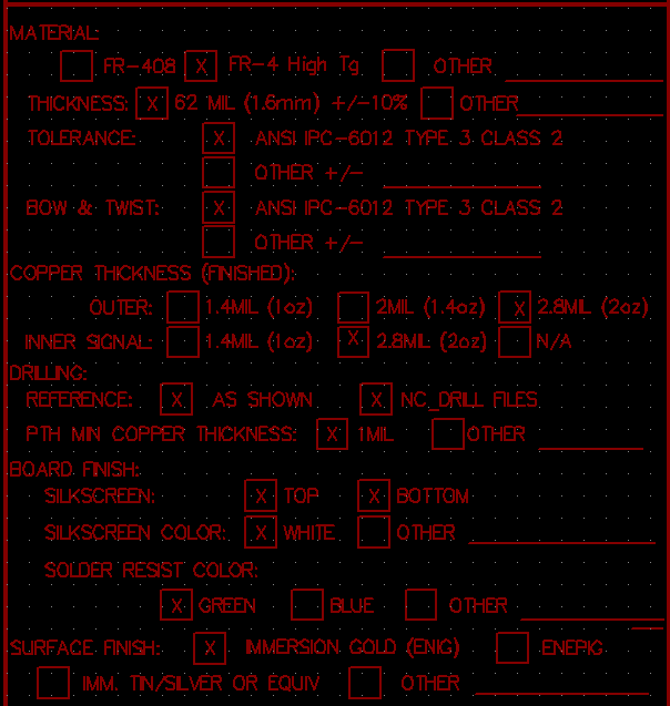
  • PCB Dimension - 10cm Max*10cm Max
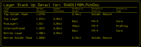
  • Layer - 4
  • PCB Thickness - 1.6mm
  • PCB Qty. - 5
  • PCB Color - Green
  • Surface Finish - ENIG
  • Copper Weight - 1oz.
  • Panelized PCBs - 1
  • Expedited Option - NO


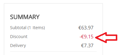
The price without shipment for this board is 65.12€. Shipping was 7.37€. The coupon got me 9.15€ off ($ 10). Totals to 63.97€

image

This design requires 2oZ copper layers. My budget can't carry the cost of such a board - so I will not be able to draw full current out of my design.

This is a compromise, one of the many I had to make. I tried to avoid compromises in the design, but did make them when ordering.

Getting a board that has enough copper on it will not require a design change. It's just ticking a different option when ordering and coughing up the monies.

I'd rather do that after I validated that I didn't make mistakes in the PCB layout.

image

image

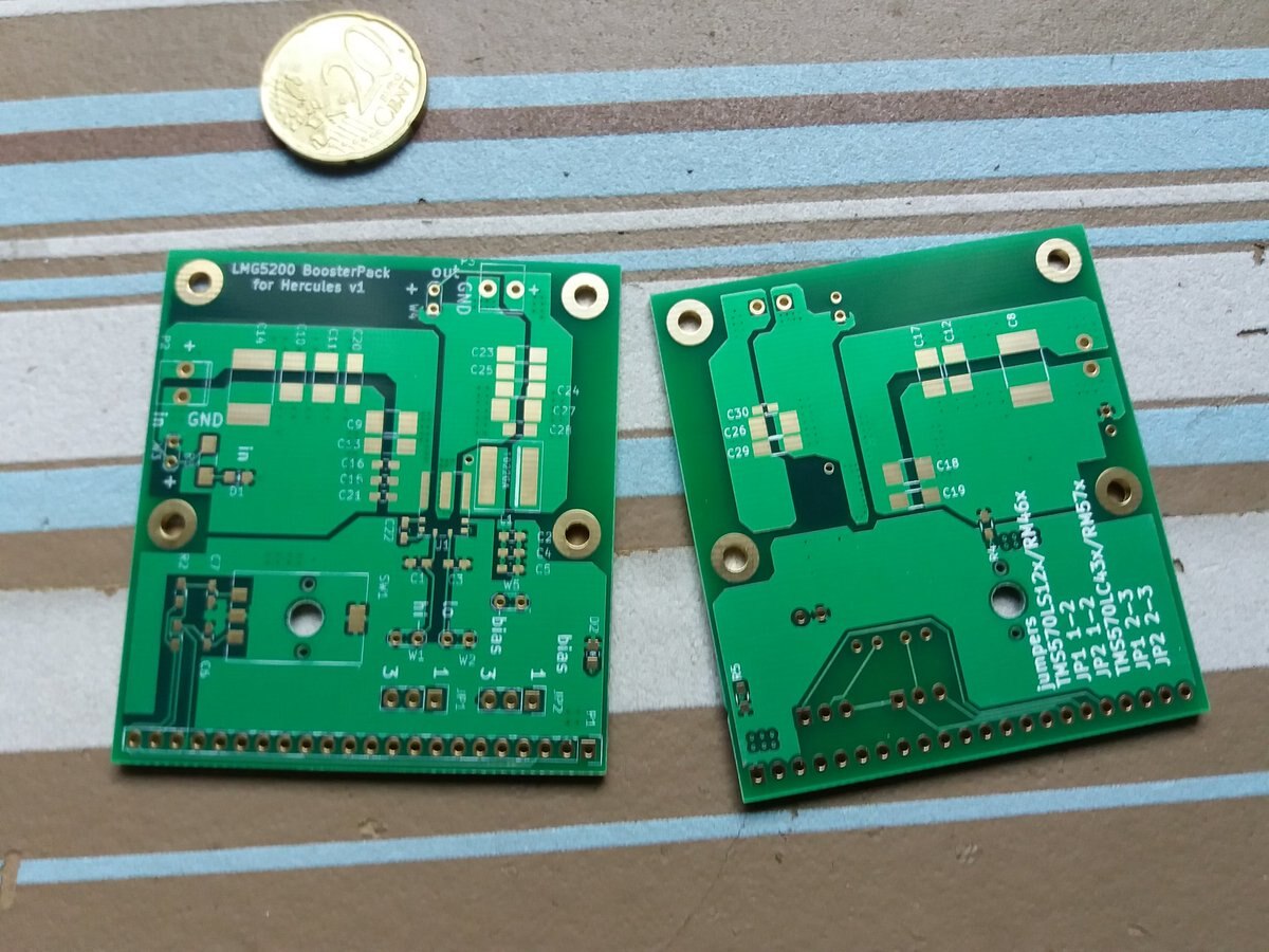
Just like previous designs I did with OSHPark, the Seeed boards look very good at first inspection.

This design is 4 layers, so I have no mechanism to look at the two inner layers. The top and bottom layer look very nice, so that's a good sign.


In the images below, the artist renditions on the left side are generated by the Seeed portal.

The photos on the right side are the actual thing. Click on them to get a detailed view.
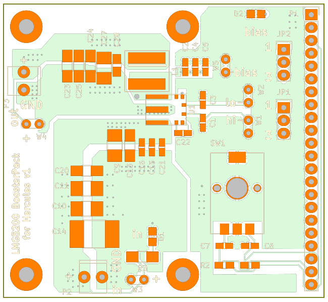
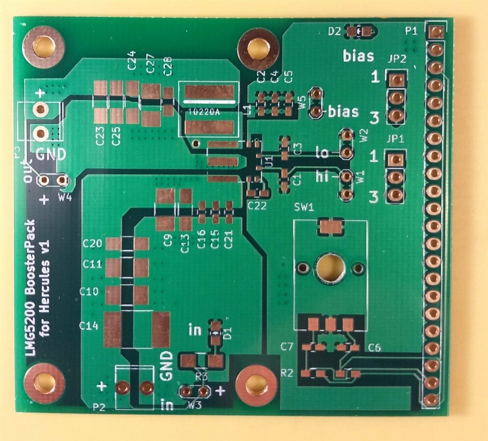
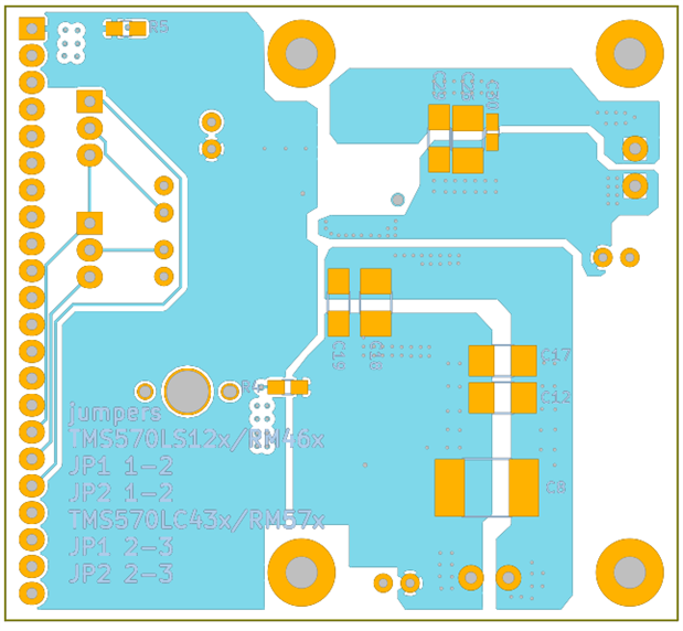
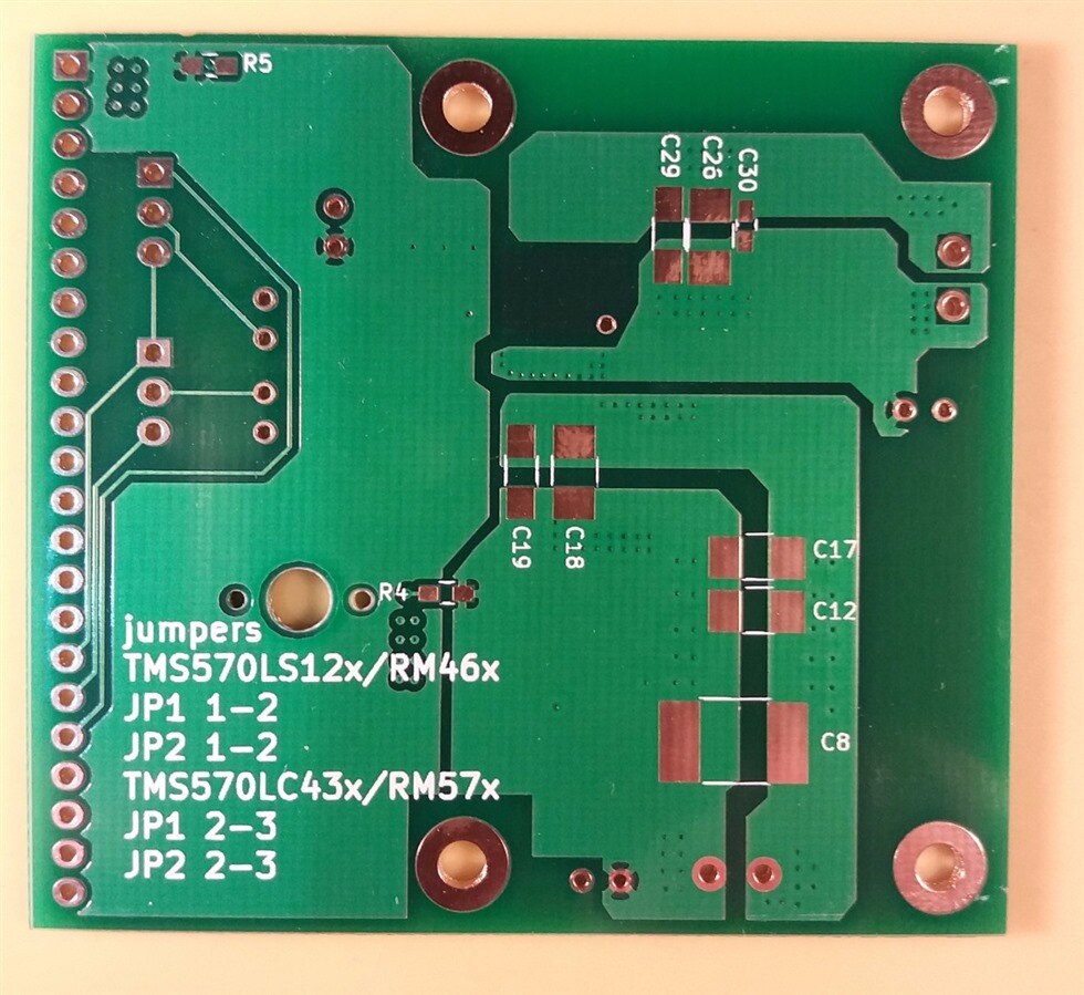
 

imageimage
imageimage


Populate Order

This is the first time I'll populate a two-sided board. I'll use hot air for the smd components.This is how I plan to approach it:

  1. solder the GaN IC and the inductor. These two have the pins under the device. I'll have to massively bombard them with heat to transfer the energy underneath where the solder paste is.
    I'll use the pre-heater that shabaz gave  me to get the whole board to a close-to-reflow temperature.
  2. then all the smd components on the bottom side. If they fll of later, that's not a big deal, because the are only few.
    I'll also use the pre-heater but on lower temperature, because its heat will be radiating on the inductor and GaN chip.
  3. Then I'll do the remaining top smd components.
    The pre-heater again on a temperature low enough to not desolder the bottom components.
  4. the trough-hole components by hand


It is my first time. I'd be happy to take your advice on the preferred order to solder the components.

The tools I have at hand:

  • hot air
  • soldering iron
  • pre-heater


You don't have permission to edit metadata of this video.
Edit media
x
image
Upload Preview
image


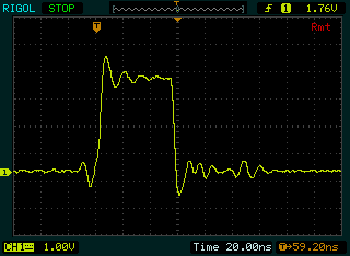
edit: I've attached the waveform of one High input pulse as hi01.wfm.

If you have a Rigol DS1052E you can upload that to your scope and examine the ringing with cursors.

image


Related Blogs
Hercules LaunchPad and GaN FETs - Part 1: Control Big Power with a Flimsy Mouse Scroll Wheel
Hercules LaunchPad and GaN FETs - Part 2: Make a BoosterPack
Hercules LaunchPad and GaN FETs - Part 3a: BoosterPack Layout - Reference Design
Hercules LaunchPad and GaN FETs - Part 3b: BoosterPack Layout - my version
Hercules LaunchPad and GaN FETs - Side Note A: BoosterPack Layout - Custom KiCad Parts
Hercules LaunchPad and GaN FETs - Side Note B: Look at the PCB
Rotary Encoders - Part 1: Electronics
Checking Out GaN Half-Bridge Power Stage: Texas Instruments LMG5200 - Part 1: Preview
Rotary Encoders - Part 4: Capturing Input on a Texas Instruments Hercules LaunchPad with eQEP
Vintage Turntable repair: Can I fix a Perpetuum Ebner from 1958 - part 4 - Hercules LaunchPad Enhanced PWM try-out
Attachments:
hi01.zip
  • Sign in to reply

Top Comments

  • michaelkellett
    michaelkellett over 8 years ago in reply to Jan Cumps +2
    Hello Jan, I do similar parts by placing the board directly onto a hotplate. I never feel sure just how hot I'm getting things if I use a hot air blower. I do use leaded solder for the lower melting point…
  • Jan Cumps
    Jan Cumps over 9 years ago +1
    The two difficult components are soldered. I've measured for solder bridges, all OK...
  • michaelkellett
    michaelkellett over 8 years ago in reply to Jan Cumps +1
    I use hotplate for four and two layer boards - not had a board problem yet. It's a cheap Chinese hotplate but the temperature regulation isn't bad. MK
Parents
  • Jan Cumps
    Jan Cumps over 8 years ago

    The board is built up, not tested yet.

    Reflow worked ok, except for 0402 and some 0603s.

    C22(0402) toombstoned, I had to rework C15, C21 and LED D2 too.

    I'm happy that the (somewhat) complex footprint of quadrature encoder - with one oval and two round mounting holes fitted perfectly.


    The two screw terminals however, P2 and P3, are a complete goof-up. The holes are too small, the distance between them is wrong and the total size of the footprints doesn't match the component.

    I have to check how that happened, because I made this footprint myself from the data sheet. (wrong part ordered or delivered, wrong drawing selected in the sheet, inch/cm switch, I don't know yet)


    image


    image

    • Cancel
    • Vote Up +1 Vote Down
    • Sign in to reply
    • More
    • Cancel
  • Jan Cumps
    Jan Cumps over 8 years ago in reply to Jan Cumps

    Two steps forward one step back at the moment.

    When I apply bias voltage to the GaN device, power supply goes trough its knees. Even if this is supposed to be a 3mA maximum. The led indicator in parallel is taking more current normally than the whole bias part.

    The LMG5200 is getting real hot too.

    I first used a DMM to check if there are shorts (I did that just after mounting the GaN and inductor too). No.


    So I have now desoldered the GaN device and will check all of the signals going there. I may have damaged the device.

    Hope not. Because I only have once IC left and they aren't cheap.


    image


    On the other side, this is a chance to go and probe the circuit without fear of damaging the GaN device...

    • Cancel
    • Vote Up 0 Vote Down
    • Sign in to reply
    • More
    • Cancel
  • Jan Cumps
    Jan Cumps over 8 years ago in reply to jc2048

    Jon Clift wrote:


    If you're reworking the board layout, you might want to give more clearance between these tracks, particularly if it might be made with 2oz copper rather than 1oz.


    Minimum track and gap is often 0.25mm (10 thou) for 2oz copper.


    I've used these settings for the non-power signals:

    image

    clearance: 0.2mm


    What is the width of the track and the height above the ground plane?

    width: 0.25mm

    height above:

    - signal lines are on the bottom layer.

    - signal gound layer is above the signal lines, both on top layer and mid layer 1 (the highest). Mid layer 2 is without copper above the signal lines.

    - board is total 1.6mm thick.

    - it's Sunday - can't calculate image, rounded to 2/3 of the thickness: approx. 1mm


    image

    • Cancel
    • Vote Up +1 Vote Down
    • Sign in to reply
    • More
    • Cancel
  • Jan Cumps
    Jan Cumps over 8 years ago in reply to jc2048

    First time tested with voltage in, without load. (yay, no explosion nor smoke)

    Here's the ripple of the output, with the scope in AC mode, 20mV/DIV.


    image


    This is DC output with a PWM duty of 44%, input 11.35V

    image

    • Cancel
    • Vote Up +1 Vote Down
    • Sign in to reply
    • More
    • Cancel
  • jc2048
    jc2048 over 8 years ago in reply to Jan Cumps

    It looked from the photo as though the spacing were less than 0.2mm.


    I had thought we could roughly calculate the impedance, but if the top is close to ground, the bottom much further away, and you have transitions from top to bottom, and go through a connector to the processor board (with a ground connection nowhere nearby), then there's no hope of calculating anything sensible.


    If the top is 0.125mm above the plane, with a 0.25mm track width, the impedance would be something of the order of 50 ohms.


    But on the bottom it's up around 100 ohms.


    That would be the case if they actually constituted transmission lines, but the top segment is short enough that that's hardly true. The transition from top to bottom is a real discontinuity (mismatch) to and isn't helping you at all.


    The best thing to do, if termination were necessary, would be to do it by experiment (just randomly pick a value between 50 and 100, and work from there).


    The layout would be better if you kept the signals on the top, though you'd still have the mess where you go across to the processor board. If you were designing both boards from scratch (for a product), you'd put a ground for the return signal right next to the signal  on the connector and not rely on a power supply ground right down the end.


    Sorry this sounds very critical. Bit late in the day - should have looked at it more closely when you posted the layout.

    • Cancel
    • Vote Up 0 Vote Down
    • Sign in to reply
    • More
    • Cancel
  • jc2048
    jc2048 over 8 years ago in reply to Jan Cumps

    So it's working. What do you think the problem was before?

    • Cancel
    • Vote Up 0 Vote Down
    • Sign in to reply
    • More
    • Cancel
  • Jan Cumps
    Jan Cumps over 8 years ago in reply to jc2048

    Jon Clift wrote:


    So it's working. What do you think the problem was before?

    I had soldered the first GaN device two times. I think it had too much heat.


    What happened:

    I put the GaN IC and the inductor as first on the board, because they are the only ones with pads under the device.

    The GaN chip reflowed nicely and the capillary effect pulled it right on the pads.

    But the inductor has a strange tendency to twist on its footprint. And it is so close to the GaN chip that it pushed it off the pads.

    (you can see in both Michael's and my photo that for both of us the inductor isn't square in its footprint:)

    image


    So I had to first heat up the GaN chip again to remove it from the board (I had to heat it for significant time before it decided to give).

    Then, after cleaning the pads and re-applying paste, I had to reflow it again, 3rd time it had a blast of hot air over it.

    Internally, this hybrid GaN device has a pcb inside its package, so that may have reflowed along the way, during the unsoldering activity.


    I have removed it again, wicked the pads, applied fresh paste and soldered the new one in place.

    • Cancel
    • Vote Up 0 Vote Down
    • Sign in to reply
    • More
    • Cancel
Comment
  • Jan Cumps
    Jan Cumps over 8 years ago in reply to jc2048

    Jon Clift wrote:


    So it's working. What do you think the problem was before?

    I had soldered the first GaN device two times. I think it had too much heat.


    What happened:

    I put the GaN IC and the inductor as first on the board, because they are the only ones with pads under the device.

    The GaN chip reflowed nicely and the capillary effect pulled it right on the pads.

    But the inductor has a strange tendency to twist on its footprint. And it is so close to the GaN chip that it pushed it off the pads.

    (you can see in both Michael's and my photo that for both of us the inductor isn't square in its footprint:)

    image


    So I had to first heat up the GaN chip again to remove it from the board (I had to heat it for significant time before it decided to give).

    Then, after cleaning the pads and re-applying paste, I had to reflow it again, 3rd time it had a blast of hot air over it.

    Internally, this hybrid GaN device has a pcb inside its package, so that may have reflowed along the way, during the unsoldering activity.


    I have removed it again, wicked the pads, applied fresh paste and soldered the new one in place.

    • Cancel
    • Vote Up 0 Vote Down
    • Sign in to reply
    • More
    • Cancel
Children
No Data
element14 Community

element14 is the first online community specifically for engineers. Connect with your peers and get expert answers to your questions.

  • Members
  • Learn
  • Technologies
  • Challenges & Projects
  • Products
  • Store
  • About Us
  • Feedback & Support
  • FAQs
  • Terms of Use
  • Privacy Policy
  • Legal and Copyright Notices
  • Sitemap
  • Cookies

An Avnet Company © 2025 Premier Farnell Limited. All Rights Reserved.

Premier Farnell Ltd, registered in England and Wales (no 00876412), registered office: Farnell House, Forge Lane, Leeds LS12 2NE.

ICP 备案号 10220084.

Follow element14

  • X
  • Facebook
  • linkedin
  • YouTube