Hi, I am new in the Eagle world and I am making a 2 layers custom board with Eagle.
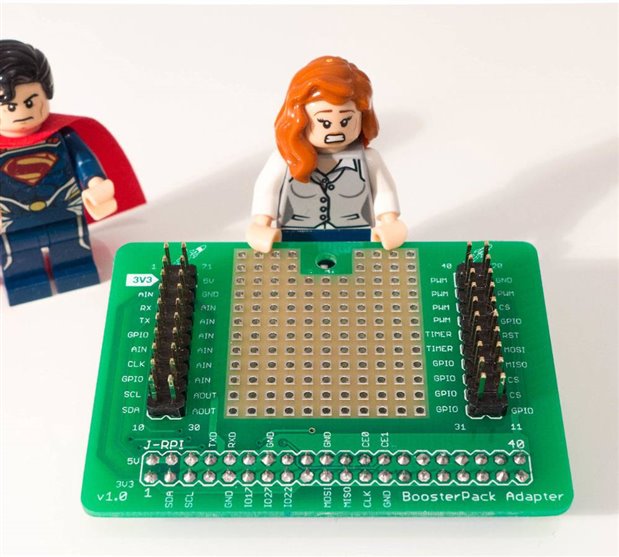
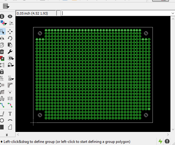
I am trying to do a simple custom size board full of holes for through hole components ( a simple prototyping board) and I am not sure about which is the best way to make the holes.
I have found many resources with totally different answers. For example on this video: https://www.youtube.com/watch?v=s4-Ugi4y9lk (min: 24.00) this guy use the simple command VIA for doing this, but a VIA should be just a connection between layers. On this discussion How to add connection points for soldered wires , another guy suggest instead the library wirepad.lbr.
This is a working project. not for fun, so I need to be quite sure that I am making the righ hole. Could you someone help me? It will be really appreciate.