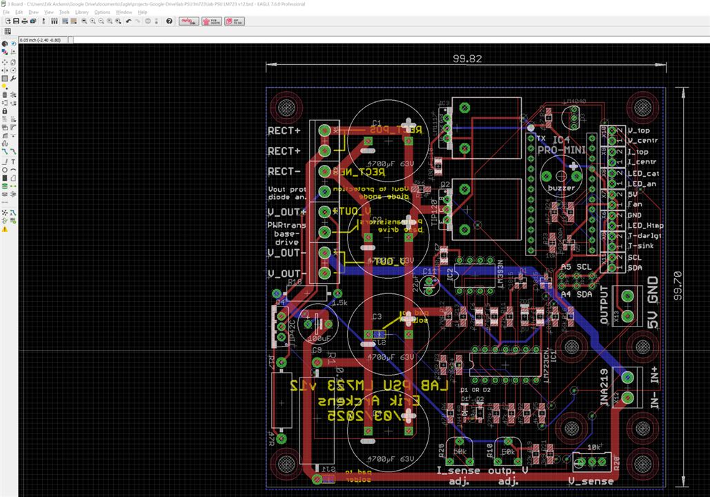
I need to get a bottom trace between two via's that currently are connected with an airwire.
However, when doing the trace at the bottom, the polygon does not cede to make way for that trace.
Using Eagle v7.6.0
How to solve?

I need to get a bottom trace between two via's that currently are connected with an airwire.
However, when doing the trace at the bottom, the polygon does not cede to make way for that trace.
Using Eagle v7.6.0
How to solve?

Hi,
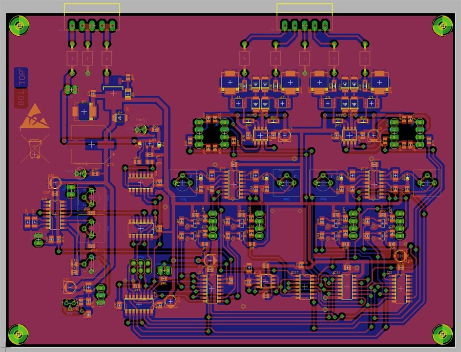
1.) your routing traces are not very ideal as well some components.
-> rotate R7, R2,
-> the traces between R7 and R5 are very critical > go another way
2.) you can switch off the polygons
-> a.) click on a polygon (on the edge off this polygon, e.g top) with the right mouse button
b.) unroute this polygon
The same do it with the other (bot polygon)
Then they are switched off and you can route your traces.
3.) switch on the polygons
-> click on the ratsnest button on eagle
4.) routing - you can change the routing strategies because this what you use is not very optimal
because the trace walks from the LM_IC far down at 45 degrees.
Actually, I use the version 9.6.0 (all versions since 5.4.0) - Fusion 360 from Autodesk
I have installed the version 6.6.0 pro, the 7.6.0 in standard version (100x80mm), and the version 9.6.0 pro.
So, I can help you with the latest version, saving the schematics as well the PCB downgrading to the version 7.0.0
-> with this you can open it with your Eagle version
KiCad – so, yes and no…
Yesterday I installed version 9.0 (I already had version 8).
The big problem is that the traces get lost when I rotate a component, for example.
The traces are not a rubber band when I move a component or a track vertex.
So, I think that is a big problem. This can cause many other problems – like, tearing apart components to traces to labels, and many other things.
Especially where everything is very close together. This makes the technician very nervous.
"Try doing that when you have to route a multilayer. Well,,,,"
Can you show the complete PCB?
Regards
Gerald
---
The 'issue' with the polygon I solved yesterday. No need to switch off the polygon, just trace the track across the polygon, do a refresh (ratsnest) and the polygon will have cleared a path for the added track.
I am not interested in 3D design features such as for libraries: mine do very well for me. And I do not want having to recreate every library in my folders.
Also, designing new packages never has been a problem for me, no issues with error codes. Eagle, for me, does what I want it to do: create schematics, libraries, and from there pcb tracing, all in a well flowing manner. To me Eagle just is a workhorse to make pcb's. Hundreds of them for over a decade.

"The 'issue' with the polygon I solved yesterday. No need to switch off the polygon, just trace the track across the polygon, do a refresh (ratsnest) and the polygon will have cleared a path for the added track."
Yes, you don't need to switch off. I just suggested it for easier working.
Refreshing the rat's nest works perfectly in Eagle Version 7.6.0, but sometimes corners and edges are visible after refreshing.
This happens when you work in "off-grid" mode, and calculation errors (rounding errors) are visible.
An unfavorable setting of the distances, fine gradation - polygon component - can also cause such rounding errors.
I always check whether I am laying the conductor tracks on the set grid and make sure that these, especially the slanted conductor tracks, are really 45.0 degrees or a multiple of that.
I always set the grid levels to be breakable down to a multiple or divisible so that the components are also placed on a grid.
-> Your autorouter is obviously set to route "off-grid" because it edges and slant the conductor tracks in such a way that it jumps around to the components.
I route mainly manually myself, including multilayer PCBs. That way I have control everywhere. Time is relative...
I also observe high frequency guidelines. Especially where there are clocks or high switched currents/voltages.
I almost never route between the component pads on SMDs, that can be critical unless it is not a problem because the distances are far enough, or the conductor does not carry any frequencies.
I try to use a direct route strategy (in cardinal directions: east-west, north-south, east-north, west-south), with as few vias as possible.
Vias next to the components are better than underneath them.
For SMDs, I make sure that I route on the top side, for through-hole components, I make sure that I route on the bottom side.

Here, the through-hole components are mountet on the bottom side (mirrored), so the tracks are on the top side.
I've all manually routed. North-south, east-west; left top power-in, right top signal-out

--
-> On your board, one of many issues:
the large electrolytic capacitors are connected to the top-layer traces.

This can cause major problems at high temperatures and under physical stress.
-> "cold solder joint", then the capacitor wobbles and you have problems, even where the conductor track breaks across.
-> How do you then repair it?
As well the "high-current" traces are very small, and they are going across the PCB. Your PCB is a power supply that can be very warm, or even hot, containing a µC module.
- So, my suggestion: connect power tracks (if there is no other option, make a power layer, or change the layer, but it is better not to lead them to the components on top) on the bottom layer side, then you have good stability and can also repair the connections better.
I have had to repair many such errors in the past, e.g. TVs, monitors with CRT screens, industrial devices, power supplies, etc...
I had to patch many burned-out holes in PCBs.
I wish you the best with your projects.
Gerald
---
"The 'issue' with the polygon I solved yesterday. No need to switch off the polygon, just trace the track across the polygon, do a refresh (ratsnest) and the polygon will have cleared a path for the added track."
Yes, you don't need to switch off. I just suggested it for easier working.
Refreshing the rat's nest works perfectly in Eagle Version 7.6.0, but sometimes corners and edges are visible after refreshing.
This happens when you work in "off-grid" mode, and calculation errors (rounding errors) are visible.
An unfavorable setting of the distances, fine gradation - polygon component - can also cause such rounding errors.
I always check whether I am laying the conductor tracks on the set grid and make sure that these, especially the slanted conductor tracks, are really 45.0 degrees or a multiple of that.
I always set the grid levels to be breakable down to a multiple or divisible so that the components are also placed on a grid.
-> Your autorouter is obviously set to route "off-grid" because it edges and slant the conductor tracks in such a way that it jumps around to the components.
I route mainly manually myself, including multilayer PCBs. That way I have control everywhere. Time is relative...
I also observe high frequency guidelines. Especially where there are clocks or high switched currents/voltages.
I almost never route between the component pads on SMDs, that can be critical unless it is not a problem because the distances are far enough, or the conductor does not carry any frequencies.
I try to use a direct route strategy (in cardinal directions: east-west, north-south, east-north, west-south), with as few vias as possible.
Vias next to the components are better than underneath them.
For SMDs, I make sure that I route on the top side, for through-hole components, I make sure that I route on the bottom side.

Here, the through-hole components are mountet on the bottom side (mirrored), so the tracks are on the top side.
I've all manually routed. North-south, east-west; left top power-in, right top signal-out

--
-> On your board, one of many issues:
the large electrolytic capacitors are connected to the top-layer traces.

This can cause major problems at high temperatures and under physical stress.
-> "cold solder joint", then the capacitor wobbles and you have problems, even where the conductor track breaks across.
-> How do you then repair it?
As well the "high-current" traces are very small, and they are going across the PCB. Your PCB is a power supply that can be very warm, or even hot, containing a µC module.
- So, my suggestion: connect power tracks (if there is no other option, make a power layer, or change the layer, but it is better not to lead them to the components on top) on the bottom layer side, then you have good stability and can also repair the connections better.
I have had to repair many such errors in the past, e.g. TVs, monitors with CRT screens, industrial devices, power supplies, etc...
I had to patch many burned-out holes in PCBs.
I wish you the best with your projects.
Gerald
---
Very useful answer! Thank you, Erik