element14 Community
element14 Community
    Register Log In
  • Site
  • Search
  • Log In Register
  • About Us
  • Community Hub
    Community Hub
    • What's New on element14
    • Feedback and Support
    • Benefits of Membership
    • Personal Blogs
    • Members Area
    • Achievement Levels
  • Learn
    Learn
    • Ask an Expert
    • eBooks
    • element14 presents
    • Learning Center
    • Tech Spotlight
    • STEM Academy
    • Webinars, Training and Events
    • Learning Groups
  • Technologies
    Technologies
    • 3D Printing
    • FPGA
    • Industrial Automation
    • Internet of Things
    • Power & Energy
    • Sensors
    • Technology Groups
  • Challenges & Projects
    Challenges & Projects
    • Design Challenges
    • element14 presents Projects
    • Project14
    • Arduino Projects
    • Raspberry Pi Projects
    • Project Groups
  • Products
    Products
    • Arduino
    • Avnet Boards Community
    • Dev Tools
    • Manufacturers
    • Multicomp Pro
    • Product Groups
    • Raspberry Pi
    • RoadTests & Reviews
  • Store
    Store
    • Visit Your Store
    • Choose another store...
      • Europe
      •  Austria (German)
      •  Belgium (Dutch, French)
      •  Bulgaria (Bulgarian)
      •  Czech Republic (Czech)
      •  Denmark (Danish)
      •  Estonia (Estonian)
      •  Finland (Finnish)
      •  France (French)
      •  Germany (German)
      •  Hungary (Hungarian)
      •  Ireland
      •  Israel
      •  Italy (Italian)
      •  Latvia (Latvian)
      •  
      •  Lithuania (Lithuanian)
      •  Netherlands (Dutch)
      •  Norway (Norwegian)
      •  Poland (Polish)
      •  Portugal (Portuguese)
      •  Romania (Romanian)
      •  Russia (Russian)
      •  Slovakia (Slovak)
      •  Slovenia (Slovenian)
      •  Spain (Spanish)
      •  Sweden (Swedish)
      •  Switzerland(German, French)
      •  Turkey (Turkish)
      •  United Kingdom
      • Asia Pacific
      •  Australia
      •  China
      •  Hong Kong
      •  India
      •  Korea (Korean)
      •  Malaysia
      •  New Zealand
      •  Philippines
      •  Singapore
      •  Taiwan
      •  Thailand (Thai)
      • Americas
      •  Brazil (Portuguese)
      •  Canada
      •  Mexico (Spanish)
      •  United States
      Can't find the country/region you're looking for? Visit our export site or find a local distributor.
  • Translate
  • Profile
  • Settings
Autodesk EAGLE
  • Products
  • More
Autodesk EAGLE
EAGLE User Support (English) Manual trace bottom track across bottom polygon: how to?
  • Blog
  • Forum
  • Documents
  • Events
  • Polls
  • Files
  • Members
  • Mentions
  • Sub-Groups
  • Tags
  • More
  • Cancel
  • New
Join Autodesk EAGLE to participate - click to join for free!
Actions
  • Share
  • More
  • Cancel
Forum Thread Details
  • State Not Answered
  • Replies 11 replies
  • Subscribers 173 subscribers
  • Views 1007 views
  • Users 0 members are here
Related

Manual trace bottom track across bottom polygon: how to?

earckens
earckens 6 months ago

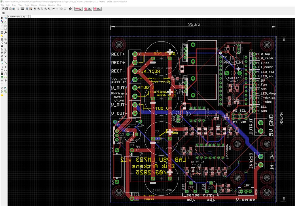
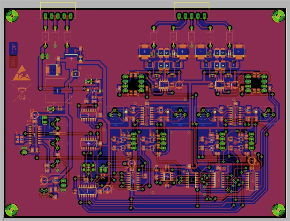
I need to get a bottom trace between two via's that currently are connected with an airwire.

However, when doing the trace at the bottom, the polygon does not cede to make way for that trace.

Using Eagle v7.6.0

How to solve?

image

  • Sign in to reply
  • Cancel

Top Replies

  • earckens
    earckens 6 months ago in reply to shabaz +1
    I got it solved: 1. from the upper right via a bottom trace to the lower left connecting track, and connect. It will then show a large yellow cross across that connection, solve it with placing a via…
  • shabaz
    shabaz 6 months ago in reply to earckens +1
    You can improve this significantly. You may say " Eagle, for me, does what I want it to do" but I think you're ignoring modern features and relying on the pretty rotten auto-router, and I can imagine the…
  • geralds
    geralds 6 months ago in reply to shabaz +1
    Hi shabaz ! Yes, many users strictly ignore modern functions. Fusion 360 (Eagle 9.6.0 on the web) has a 3D function, has a "modern" autor-outer, but ... so far, I like manual routing - it's a training…
Parents
  • geralds
    0 geralds 6 months ago

    Hi,

    1.) your routing traces are not very ideal as well some components.

    -> rotate R7, R2, 

    -> the traces between R7 and R5 are very critical > go another way

    2.) you can switch off the polygons

    -> a.) click on a polygon (on the edge off this polygon, e.g top) with the right mouse button

    b.) unroute this polygon

    The same do it with the other (bot polygon)

    Then they are switched off and you can route your traces.

    3.) switch on the polygons

    -> click on the ratsnest button on eagle 

    4.) routing - you can change the routing strategies because this what you use is not very optimal

    because the trace walks from the LM_IC far down at 45 degrees.

    Actually, I use the version 9.6.0 (all versions since 5.4.0) - Fusion 360 from Autodesk

    I have installed the version 6.6.0 pro, the 7.6.0 in standard version (100x80mm), and the version 9.6.0 pro.

    So, I can help you with the latest version, saving the schematics as well the PCB downgrading to the version 7.0.0

    -> with this you can open it with your Eagle version

    KiCad – so, yes and no…

    Yesterday I installed version 9.0 (I already had version 8).

    The big problem is that the traces get lost when I rotate a component, for example.

    The traces are not a rubber band when I move a component or a track vertex.

    So, I think that is a big problem. This can cause many other problems – like, tearing apart components to traces to labels, and many other things.

    Especially where everything is very close together. This makes the technician very nervous.

    "Try doing that when you have to route a multilayer. Well,,,,"

    Can you show the complete PCB?

    Regards 

    Gerald

    ---

    • Cancel
    • Vote Up 0 Vote Down
    • Sign in to reply
    • Verify Answer
    • Cancel
  • earckens
    0 earckens 6 months ago in reply to geralds

    The 'issue' with the polygon I solved yesterday. No need to switch off the polygon, just trace the track across the polygon, do a refresh (ratsnest) and the polygon will have cleared a path for the added track.

    I am not interested in 3D design features such as for libraries: mine do very well for me. And I do not want having to recreate every library in my folders.

    Also, designing new packages never has been a problem for me, no issues with error codes. Eagle, for me, does what I want it to do: create schematics, libraries, and from there pcb tracing, all in a well flowing manner. To me Eagle just is a workhorse to make pcb's. Hundreds of them for over a decade.

    image

    • Cancel
    • Vote Up 0 Vote Down
    • Sign in to reply
    • Verify Answer
    • Cancel
Reply
  • earckens
    0 earckens 6 months ago in reply to geralds

    The 'issue' with the polygon I solved yesterday. No need to switch off the polygon, just trace the track across the polygon, do a refresh (ratsnest) and the polygon will have cleared a path for the added track.

    I am not interested in 3D design features such as for libraries: mine do very well for me. And I do not want having to recreate every library in my folders.

    Also, designing new packages never has been a problem for me, no issues with error codes. Eagle, for me, does what I want it to do: create schematics, libraries, and from there pcb tracing, all in a well flowing manner. To me Eagle just is a workhorse to make pcb's. Hundreds of them for over a decade.

    image

    • Cancel
    • Vote Up 0 Vote Down
    • Sign in to reply
    • Verify Answer
    • Cancel
Children
  • geralds
    0 geralds 6 months ago in reply to earckens

    "The 'issue' with the polygon I solved yesterday. No need to switch off the polygon, just trace the track across the polygon, do a refresh (ratsnest) and the polygon will have cleared a path for the added track."

    Yes, you don't need to switch off. I just suggested it for easier working.

    Refreshing the rat's nest works perfectly in Eagle Version 7.6.0, but sometimes corners and edges are visible after refreshing.
    This happens when you work in "off-grid" mode, and calculation errors (rounding errors) are visible.
    An unfavorable setting of the distances, fine gradation - polygon component - can also cause such rounding errors.

    I always check whether I am laying the conductor tracks on the set grid and make sure that these, especially the slanted conductor tracks, are really 45.0 degrees or a multiple of that.
    I always set the grid levels to be breakable down to a multiple or divisible so that the components are also placed on a grid.

    -> Your autorouter is obviously set to route "off-grid" because it edges and slant the conductor tracks in such a way that it jumps around to the components.

    I route mainly manually myself, including multilayer PCBs.
    That way I have control everywhere. Time is relative...

    I also observe high frequency guidelines. Especially where there are clocks or high switched currents/voltages.

    I almost never route between the component pads on SMDs, that can be critical unless it is not a problem because the distances are far enough, or the conductor does not carry any frequencies.
    I try to use a direct route strategy (in cardinal directions: east-west, north-south, east-north, west-south), with as few vias as possible.

    Vias next to the components are better than underneath them.

    For SMDs, I make sure that I route on the top side, for through-hole components, I make sure that I route on the bottom side.

    PCB1

    Here, the through-hole components are mountet on the bottom side (mirrored), so the tracks are on the top side.
    I've all manually routed. North-south, east-west; left top power-in, right top signal-out

    PCB1-polygon

    --

    -> On your board, one of many issues:
    the large electrolytic capacitors are connected to the top-layer traces.

    image

    This can cause major problems at high temperatures and under physical stress.
    -> "cold solder joint", then the capacitor wobbles and you have problems, even where the conductor track breaks across.
    -> How do you then repair it?

    As well the "high-current" traces are very small, and they are going across the PCB. Your PCB is a power supply that can be very warm, or even hot, containing a µC module.  

    - So, my suggestion: connect power tracks (if there is no other option, make a power layer, or change the layer, but it is better not to lead them to the components on top) on the bottom layer side, then you have good stability and can also repair the connections better.
    I have had to repair many such errors in the past, e.g.
    TVs, monitors with CRT screens, industrial devices, power supplies, etc...
    I had to patch many burned-out holes in PCBs.

    I wish you the best with your projects.

    Gerald

    ---

    • Cancel
    • Vote Up 0 Vote Down
    • Sign in to reply
    • Verify Answer
    • Cancel
  • shabaz
    0 shabaz 6 months ago in reply to earckens

    You can improve this significantly. You may say "Eagle, for me, does what I want it to do" but I think you're ignoring modern features and relying on the pretty rotten auto-router, and I can imagine the performance will be bad. Your PCB is on version 12.. that's not normal.

    Anyway, if you think you're doing fine then I'm not going to interfere.

    • Cancel
    • Vote Up +1 Vote Down
    • Sign in to reply
    • Verify Answer
    • Cancel
  • earckens
    0 earckens 6 months ago in reply to geralds

    Very useful answer! Thank you, Erik

    • Cancel
    • Vote Up 0 Vote Down
    • Sign in to reply
    • Verify Answer
    • Cancel
  • geralds
    0 geralds 6 months ago in reply to shabaz

    Hi shabaz!

    Yes, many users strictly ignore modern functions.

    Fusion 360 (Eagle 9.6.0 on the web) has a 3D function, has a "modern" autor-outer, but ... so far, I like manual routing - it's a training for my brain.

    One of the best autor-routers I've worked with was this one from PCAD - now actually an Altium.
    But Altium is extremely expensive, as is Autodesk. Well, you have to specialize somewhere, and that's what I did with Eagle - Fusion 360.

    KiCad has great features now.
    I'll also be switching to KiCad soon - 2026, when Autodesk will no longer support Eagle in the offline version (Cadsoft version).
    Until then, or even sooner, if:

    I really want the connection of the components to the wires to be electrically fixed and that the traces are real rubber bands.
    Every time you move them, then they dissolve into lines.
    Traces should be treated as traces. Eagle does that very well.
    Eagle treats wires/traces strictly separately from drawn lines, just like Altium's PCAD (since 1985, my first ECAD I worked with).

    The gimmicks with a super-great library, with or without 3D components, are very good so far, I also like playing with it, I'm currently building up a decent library, but it's not really necessary for a real product.
    Electrically!
    There must be no errors.
    Unfortunately, only a few software manufacturers can program it properly.

    Yes, I also look at costs, of course, but I understand that everything costs something somewhere.

    It should just be fair.

    I'm curious to see what KiCad will bring this year when I read these explanations and update descriptions on their website.

    • Cancel
    • Vote Up +1 Vote Down
    • Sign in to reply
    • Verify Answer
    • Cancel
  • earckens
    0 earckens 6 months ago in reply to geralds

    Great explanation, thank you geralds.

    Personnaly I abhor Autocad's tendency to bring (in my view) superfluous version updates. And especially their policy of not allowing offline work. I also do 3D design, and use Freecad. I had a look at Autocad's 3D programs but turned off when realising they only work online.

    To each his own :).

    • Cancel
    • Vote Up 0 Vote Down
    • Sign in to reply
    • Verify Answer
    • Cancel
  • shabaz
    0 shabaz 6 months ago in reply to geralds

    Hi Gerald,

    I'm the same, I prefer manual routing; I meant that modern features for guided routing in KiCad are better than the poor auto-router in EAGLE. I don't mean auto-router is better than manual routing (at least, not for the complexity of boards one would be using these particular tools for).

    I've not seen what improvements KiCad 9 has made (I don't think they have the rubber-banding feature you mention). In v8, there's a kind of slight approximation, which is the auto-complete. It allows you to move a part, and all connections will turn to air-wires as you mention; however, if you then press Shift-F (with the component highlighted), it will try to auto-fix the connections, i.e. the end result of a rubber-banding sort of operation. Here's a video of it, where I moved a part, and then deleted the traces that I didn't like to remain, and then selected the component and pressed Shift-F. Not as smooth as rubber-banding of course. You can see it missed one trace, but that's easy to fix, by clicking on that trace and pressing Shift-F again.

    Personally I don't use this tool in this way (I sometimes use it per track, using just the 'F' key). For general routing, I usually have KiCad set to the 'walk around' mode, and find that very useful minimal guidance while routing (but the other options are very useful too).

    You don't have permission to edit metadata of this video.
    Edit media
    x
    image
    Upload Preview
    image

    The EAGLE imports of libraries is already excellent in v8, however since EAGLE had issues with slotted pads and shaped pads, it is beneficial to either try to clean up those specific footprints, or to recreate them, using the direct KiCad support for those features.

    But it would be wise to retain old EAGLE for old projects for sure (even though, again, KiCad support of EAGLE project import is pretty good too).

    Personally, I've over time just redone the footprints that I wanted to use, rather than use the EAGLE version (however, I have still imported the EAGLE footprints, so I can easily compare, to reduce the risk of error).

    Regarding the 3D models, I now try to always have a 3D model for each new component I add, simply because I've found it reduces errors so much, in two ways:

    (1) The obvious way, which is that you can easily see if there are clashes between parts on the board, and optimize the position of parts on board edges, etc.

    (2) Not-so-obvious (at least not initially to me!) - it greatly reduces the risk of error in the PCB footprint creation process in the first place, because, if your 3D model doesn't match the pads and outline, then it's immediately clear there is an error in the footprint or the model! This has been immensely useful, because often some dimensions may be vague or missing in the drawings in the datasheets, or I may have introduced some accidental error. The 3D model lets me instantly get a decent amount of additional confidence that the footprint is good.

    • Cancel
    • Vote Up 0 Vote Down
    • Sign in to reply
    • Verify Answer
    • Cancel
element14 Community

element14 is the first online community specifically for engineers. Connect with your peers and get expert answers to your questions.

  • Members
  • Learn
  • Technologies
  • Challenges & Projects
  • Products
  • Store
  • About Us
  • Feedback & Support
  • FAQs
  • Terms of Use
  • Privacy Policy
  • Legal and Copyright Notices
  • Sitemap
  • Cookies

An Avnet Company © 2025 Premier Farnell Limited. All Rights Reserved.

Premier Farnell Ltd, registered in England and Wales (no 00876412), registered office: Farnell House, Forge Lane, Leeds LS12 2NE.

ICP 备案号 10220084.

Follow element14

  • X
  • Facebook
  • linkedin
  • YouTube