Application Note
EMC & Efficiency Optimization of High Power DC/DC Converters
ANP049 BY ANDREAS NADLER
1 Introduction
Choosing the appropriate capacitor technology, storage inductors, switching frequency and semiconductors, among other factors, is vital for the efficiency of DC/DC switching regulators with relatively high input and output currents. A high-efficiency switching regulator is market-ready if it, and the end product in which it is used, comply with all necessary EMC standards. This often means that further appropriate filters must be included at the input and output to reduce emissions of interference. However, with high input and output currents, it is difficult to find a compromise between the efficiency, size, damping and cost of the filter, and the actual performance level. This document will use the example of a 100 W buck-boost DC/DC design to outline the considerations, layout and components necessary to find such a compromise.

Figure 1: Demonstration circuit board for a 100 W buck-boost converter.
2 Scope of Project
A buck-boost converter is to be developed, meeting the following requirements:
- Up to 100 W Pout at 18 Vout / Vin 14-24 Vdc --> Iin max. = 7 A --> Iout max. 5.55 A
- Efficiency in excess of 95 % at 100 W output
- Compliance with CISPR32 class B emissions limits (conducted and radiated)
- Low residual ripple of output voltage (below 20 mVpp)
- Shielding not possible
- Long cable at input and output (1 m each)
- As compact as possible
- As cost-effective as possible
Due to these strict requirements, it is essential to develop a very low-inductive and compact layout, and filters harmonized with the converter. If we consider EMC, the cables at the input and output are the main antennas in the frequency range up to 1 GHz. Because modern 4-switch buck-boost converters have high-frequency current loops at the input as well as the output, depending on the operating mode, both the input and the output must be filtered. This prevents high-frequency interference, resulting from rapid switching of the MOSFETs, from passing into the cables and being radiated.

Figure 2: Circuit diagram of the high-frequency ΔI/Δt loops and the critical ΔU/Δt switching nodes, depending on the operating mode of the converter.
A switching regulator from Linear Technology (Analog Devices) was used for this AppNote: LT3790. This has an input voltage range of up to 60 VDC, adjustable switching frequency, and can control four external MOSFETs. This ensures a high degree of flexibility in the design.
3 Design & Measurements
Key Features of the Buck-Boost Design:
- Double-sided, 6-layer printed circuit board
- 400 kHz switching frequency
- Current ripple in choke approx. 30 % of rated current
- Compact 60 V MOSFETS with low Rdson, Rth and package ESL
- 1 Ω gate series resistors

Figure 3: Simplified diagram of the converter power stage.
3.1. Inductor selection
The appropriate inductor can be quickly, easily and precisely selected with the help of the REDEXPERT online platform. In this case, the operating parameters (Vin, fsw, Iout, Vout, ΔI ) must be entered once for buck operation, and again for boost operation. In buck operation, this gives a larger inductance and a smaller maximum peak current (7.52 µH / 5.83 A). In boost operation, the inductance is smaller, but the maximum peak current is higher (4.09 µH / 7.04 A). A further advantage of choosing inductors with REDEXPERT is that different components can be compared on the basis of their complex AC and DC losses and the resulting component heating, as well as on their obvious data (size, rated current, etc.). In this case, a shielded inductor from the WE-XHMI series with 6.8 µH inductance and 15 A rated current was selected. The component has a very low RDC and extremely compact dimensions of just 15x15x10 mm (L/W/H), thanks to modern manufacturing technology. The innovative core material mixture also gives soft and temperature-independent saturation characteristics.
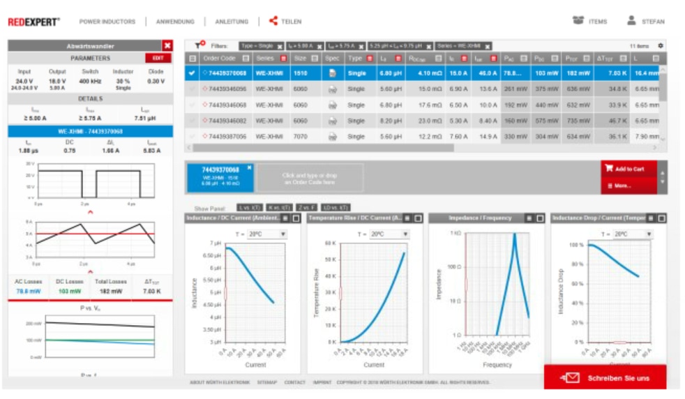
Figure 5: REDEXPERT simulation (buck operation) of WE-XHMI 74439370068.

Figure 6: REDEXPERT graphs of impedance, ESR und DC Bias of the chosen MLCC
3.2. Input capacitors selection
The high pulse currents through the blocking capacitors and the required low residual ripple make a combination of aluminum polymer and ceramic capacitors the best choice. Once the maximum input and output voltage ripple has been set, the required capacitances can be calculated using the following formulae.

Chosen: 6 x 4.7µF / 50V / X7R = 28.2 µF
(WCAP-CSGP 885012209048)
REDEXPERT allows the DC bias of the MLCCs to be quickly and easily established, resulting in a value significantly closer to reality, see figure 6. Result: 20 % less capacitance at an input voltage of 24 V must be expected; this gives an effective capacitance of only 23 µF, though this is still sufficient. A 68 µF / 35 V WCAP-PSLC aluminum polymer capacitor is also used parallel to the ceramic capacitors, with a 0.22 Ω SMD resistor wired in series. This serves to maintain stability with respect to the converter's negative input impedance together with the input filter (see ANP044 for more information). Since this capacitor is also subjected to a certain amount of high pulse current, an aluminum electrolytic capacitor is less suitable in this case. The higher ESR would cause such a capacitor to become very hot.
3.3. Selection of Output capacitors

Chosen: 6 x 4.7 µF / 50 V / X7R = 28.2 µF – 15 % DC bias = 24 µF
(WCAP-CSGP 885012209048)
Plus: 1 x aluminum polymer capacitor for sufficiently fast responsiveness to transients:
WCAP-PSLC 220 µF / 25 V

Figure 7: Circuit diagram of 100 W buck-boost converter, including all filter components.
3.4. Analysis of Layout on PCB top layer

Figure 8: EMC-optimized layout of the top layer for the buck-boost converter (input and output filter banks omitted).
1. Close arrangement of the ceramic blocking capacitors makes the input and output loops, with high, ΔI/Δt very compact.
2. Separate and smooth AGND copper surface for the sensitive, high-impedance analogue part of the circuit (connected to PGND at PIN30 only).
3. Compact bootstrap circuit very close to the switching regulator IC.
4. Current measurement connections to the shunts are routed as differential lines and have a clean Kelvin connection.
5. Broadband pi filter to decouple the internal power supply of the switching regulator IC.
6. Use of as many vias as possible for low-inductance and low-impedance connections to the underside of the circuit board and the inner PGND layers.
7. Large areas of copper make an excellent heat sink and provide low RDC, but they must not be any larger than necessary – especially on the two ´hot´ΔU/Δt switching nodes – to avoid forming undesired antennas.
3.5. Analysis of Layout on PCB bottom layer

Figure 9: EMC-optimized layout of the bottom layer of the buck-boost converter, with four power MOSFETs, the remaining blocking capacitors, the shunt and the freewheeling diodes.
8. Arrangement of the ceramic blocking capacitors close to the FETs makes the input and output loops with high, ΔI/Δt very compact.
9. The geometric layout and the use of copper surfaces mean that the connections among the FETs and between the FETs and the shunt have very low impedance and induction.
10.Current shunt with reverse geometry for even lower parasitic inductance; the HF current loop is thus minimal as well.
11.Better cooling of the semiconductors is possible on the PCB underside, as there are no further large components to impede thermal connection.
12.Ultrafast recovery Schottky diodes are placed immediately next to the corresponding FETs.
13. Large areas of copper make an excellent heat sink and provide low RDC, but they must not be any larger than necessary – especially on the two ´hot´ΔU/Δt switching nodes – to avoid forming undesired antennas.
3.6. Analysis of Layout in Intermediate Layers
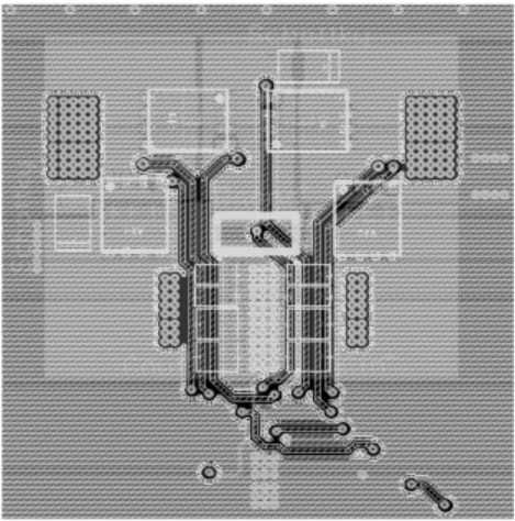
Figure 10: Layout of intermediate layer 3.
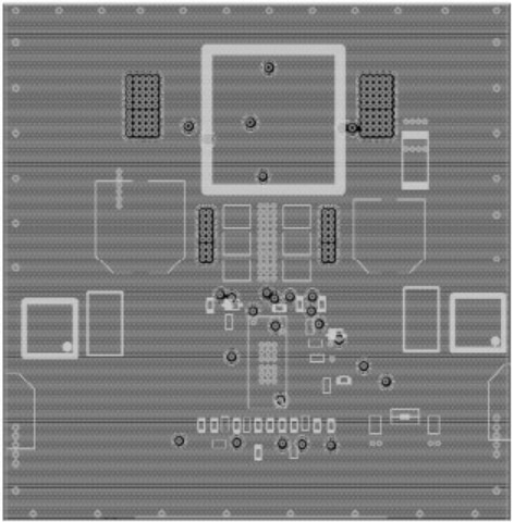
Figure 11: Layout of intermediate layers 2, 4 and 5
- All 4 intermediate layers are essentially PGND copper surfaces, giving corresponding benefits:
- Uniform distribution of thermal loss.
- Current feed and return paths always form as small a loop area as possible, minimizing resulting EMC-critical loop antennas.
- A certain amount of EMC-critical HF is converted to heat to in the PGND surfaces (eddy current effect) and thus absorbed. This effect increases as the distance between the PGND and the HF-critical components decreases.
- Partial shielding.
- The leads to the gates of the MOSFETs run within two PGND layers and are thus completely shielded.
- Vias with GND potential are placed at regular intervals around the edge of the PGND. These counteract potential edge radiation.
3.7. Components for Input & Output Filters
The components for the filters must be selected so that broadband interference suppression of 150 kHz – 300 MHz can be achieved. This should adequately damp the expected conducted and radiated EMC interference. However, the filter can be simplified if the cables used at the input or output are shortened or omitted.
3.8. EMC Measurements without Filter (100 W Pout)
To satisfy the needs of most applications, the converter's interference should be within the limits of class B (domestic), both in the conducted (150 kHz – 30 MHz) and the radiated (30 MHz – 1 GHz) ranges, see figure 12 and 13. As well as the insertion loss, it is especially important – with the currents required here – that the inductive components have as low an RDC as possible to keep efficiency and self-heating at an acceptable level. Low RDC unfortunately often means a larger design as well. Therefore, it is particularly important to use state-of-the-art components here as well, which provide an excellent compromise between RDC, impedance and size. The WE-MPSB series is particularly suitable in this case, as well as compact designs from the WE-XHMI series. Inexpensive aluminum electrolytic capacitors (such as WCAP-ASLI) are suitable as capacitive components for filters above 10µF capacitance. Unlike the blocking capacitors mentioned above, high ripple currents do not occur here (filter inductance effectively blocks these currents) and so they do not have to be suitable for high ripple currents. Higher ESR is therefore not a problem. This even helps to keep the filter factor low and thus prevents further unwanted oscillations.
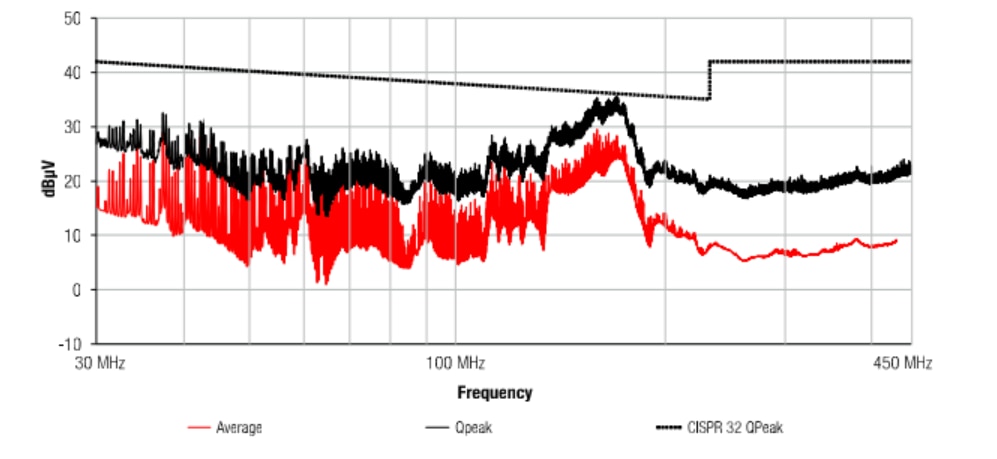
Figure 12: Measurement of conducted interference WITHOUT input filter. As expected, interference is not within class B limits, despite a good layout.
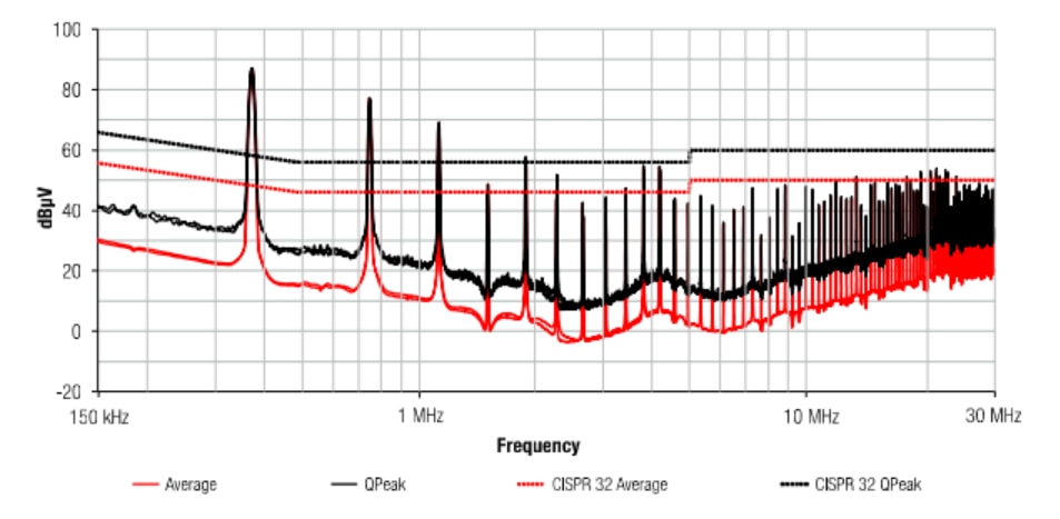
Figure 13: Measurement of radiated interference WITHOUT input and output filters. The difference between the interference and the limit value is very small at approximately 180MHz, which can cause problems with subsequent measurements. The cause is the fast reverse recovery time of the Schottky recovery current, which stimulates parasitic LC resonance.

Figure 14: Block diagram of filter elements for three different frequency ranges.
Figure 15 shows the structure of the input and output filter (for common mode and differential mode). Figure 16 illustrates the simulated differential mode insertion damping of this filter across the frequency range relevant for EMC.

Figure 15: LTSpice simulation for differential mode insertion damping of the input and output filter bank (only the leakage inductance is relevant for the CMC).

Figure 16: Simulated differential insertion attenuation with parasitic characteristics of the two filter banks. Up to 500MHz an insertion loss of more than 80dB can be achieved.
The additional filter losses result from ohmic losses in the inductors:
- Losses at output filter: I² x Rdc = 5.5 A² x 30mΩ = 907 mW
- Losses at input filter: I² x Rdc = 7 A² x 18.4mΩ = 902 mW
The selection criteria for the current-compensated chokes were:
- Maximum possible common mode impedance over a wide frequency range (150 kHz to 300 MHz, in this case).
- Sectional winding technology for as much leakage inductance as possible (differential mode interference suppression).
- Low RDC.
- Compact design and SMT.
3.9. Analysis of Layout on PCB Upper Surface with Input & Output Filter
1. Both filter banks are arranged so that inductive and capacitive coupling with the main part of the circuit is eliminated as much as possible; this could otherwise compromise the filter effect.
2. The PGND copper surfaces in the inner layers are connected only to the two aluminum electrolytic capacitors of the filter. There is no copper below the filter banks, even in the intermediate layers. This avoids galvanic coupling, which would reduce the suppression effect of the filter capacitors.
3. The T-filters are designed so that unwanted capacitive and inductive couplings within the three components are eliminated as much as possible.
4. No copper is placed under the two current compensating chokes to minimize capacitive coupling

Figure 17: Common mode and differential mode impedance curves of the two WE-UCF current-compensated chokes used

Figure 18: View of TOP layer, including all filter elements for compliance with CISPR32 class B

Figure 19: Measurement of TOP layer
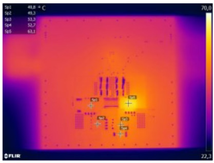
Figure 20: Measurement of BOTTOM layer
3.10. Measurement of Temperature and Efficiency with Filter at 100 W Pout (Ta = 22 °C)
Measured efficiency at 100 W Pout:
- Buck mode 96.5 %
- Boost mode 95.6 %
The maximum component temperature is below 64 °C, which gives enough allowance for higher ambient temperatures and means low stress on the components. Efficiency is likewise at a very high level, especially considering that this factors into all the filter components
4. Summary
Despite an elaborate layout and appropriate active and passive components, the demanding specifications of this example (long cables, lack of shielding, etc.) mean that class B compliance is impossible without further, additional filters. However, because this was to be expected, it was possible to design in suitable filters from the outset. Thus, a flexible, highly efficient and class B compliant 100 W buck-boost converter has been developed. To create an even more compact circuit board, the two filter banks could, for example, be turned through 90° or positioned on the underside of the PCB. Results can be achieved quickly and inexpensively with the help of design and simulation software such as REDEXPERT and LTSpice.

Figure 21: Conducted interference WITH the input filters as specified above. Both the average and the quasi peak interference are within the specified limits across the entire measured range.
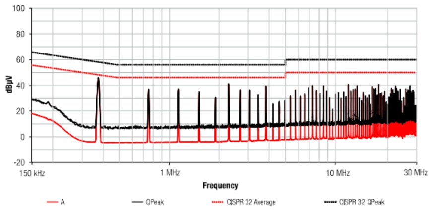
Figure 22: Radiated interference WITH the input and output filters as specified above. Interference is sufficiently within the specified limit (horizontally and vertically) across the entire measured range.
A. Appendix
A.1. Bill of Material

A.2. References
ANP044: Negative Input Resistance of Switching Regulators
I M P O R T AN T N O T I C E
The Application Note is based on our knowledge and experience of typical requirements concerning these areas. It serves as general guidance and should not be construed as a commitment for the suitability for customer applications by Würth Elektronik eiSos GmbH & Co. KG. The information in the Application Note is subject to change without notice. This document and parts thereof must not be reproduced or copied without written permission, and contents thereof must not be imparted to a third party nor be used for any unauthorized purpose. Würth Elektronik eiSos GmbH & Co. KG and its subsidiaries and affiliates (WE) are not liable for application assistance of any kind. Customers may use WE’s assistance and product recommendations for their applications and design. The responsibility for the applicability and use of WE Products in a particular customer design is always solely within the authority of the customer. Due to this fact it is up to the customer to evaluate and investigate, where appropriate, and decide whether the device with the specific product characteristics described in the product specification is valid and suitable for the respective customer application or not. The technical specifications are stated in the current data sheet of the products. Therefore the customers shall use the data sheets and are cautioned to verify that data sheets are current. The current data sheets can be downloaded at www.we-online.com. Customers shall strictly observe any product-specific notes, cautions and warnings. WE reserves the right to make corrections, modifications, enhancements, improvements, and other changes to its products and services. WE DOES NOT WARRANT OR REPRESENT THAT ANY LICENSE, EITHER EXPRESS OR IMPLIED, IS GRANTED UNDER ANY PATENT RIGHT, COPYRIGHT, MASK WORK RIGHT, OR OTHER INTELLECTUAL PROPERTY RIGHT RELATING TO ANY COMBINATION, MACHINE, OR PROCESS IN WHICH WE PRODUCTS OR SERVICES ARE USED. INFORMATION PUBLISHED BY WE REGARDING THIRD-PARTY PRODUCTS OR SERVICES DOES NOT CONSTITUTE A LICENSE FROM WE TO USE SUCH PRODUCTS OR SERVICES OR A WARRANTY OR ENDORSEMENT THEREOF. WE products are not authorized for use in safety-critical applications, or where a failure of the product is reasonably expected to cause severe personal injury or death. Moreover, WE products are neither designed nor intended for use in areas such as military, aerospace, aviation, nuclear control, submarine, transportation (automotive control, train control, ship control), transportation signal, disaster prevention, medical, public information network etc. Customers shall inform WE about the intent of such usage before design-in stage. In certain customer applications requiring a very high level of safety and in which the malfunction or failure of an electronic component could endanger human life or health, customers must ensure that they have all necessary expertise in the safety and regulatory ramifications of their applications. Customers acknowledge and agree that they are solely responsible for all legal, regulatory and safety-related requirements concerning their products and any use of WE products in such safety-critical applications, notwithstanding any applications-related information or support that may be provided by WE. CUSTOMERS SHALL INDEMNIFY WE AGAINST ANY DAMAGES ARISING OUT OF THE USE OF WE PRODUCTS IN SUCH SAFETY-CRITICAL APPLICATIONS.
DIRECT LINK
ANP049: EMC & Efficiency Optimization of High Power DC/DC Converter
USEFUL LINKS:
Application Notes : https://we-online.com/en/support/knowledge/application-notes
Services: https://we-online.com/en/products/components/service
Contact : https://we-online.com/en/support/contact
CONTACT INFORMATION
Würth Elektronik eiSos GmbH & Co. KG
Max-Eyth-Str. 1, 74638 Waldenburg, Germany
Tel.: +49 (0) 7942 / 945 – 0
Email: appnotes@we-online.de

.jpg-1440x400x2.jpg?sv=2016-05-31&sr=b&sig=pi0O33EKmBiC57r2qUf8h1b103767HyXAEwV6GBBBlo%3D&se=2026-04-03T23%3A59%3A59Z&sp=r&_=AA2zJplAeKRxyglTon80Jw==)