Application Notes
Feedback loop compensation of a current-mode Flyback converter with optocoupler
ANP113 by Eleazar Falco
01. INTRODUCTION AND THEORETICAL BACKGROUND
The flyback converter is an isolated switching power supply topology widely used for output power levels below 150 W (Figure 1). In addition to providing galvanic isolation between input and output, it generates an output voltage which can be higher or lower than the input voltage. Its range of applications is vast, covering not only offline AC-DC conversion and power factor correction stages, but also high and low-voltage DC-DC converters alike in virtually all industry areas. A few example applications are main and auxiliary supplies for home-appliances, battery chargers for smartphones/tablets, LED lighting, computer/laptop power supplies, power-over-ethernet (PoE), industrial power, auxiliary supplies in motor drives, etc.
To keep the output voltage regulated at a target level despite variations in the input voltage or output current, the output voltage needs to be monitored and a related signal fed back to the controller, which can then adjust the duty-cycle of the control transistor regulating with it the flow of energy to the output. This is a closed-loop negative feedback system, with a plant block (formed by the duty-cycle generator and power stage), and with a compensator block, necessary to stabilize and shape the dynamic response of the converter (see Figure 2). Note that the compensator is designed to ensure not only that the feedback loop is stable, meaning that perturbation signals will not generate a sustained oscillation in the system, but also that after a transient event the output voltage will meet the target requirements regarding over- and undershoot, ringing and settling-time imposed by the supplied load.
In most isolated converters requiring tight output voltage regulation, an optocoupler is commonly used to transfer the feedback signal across the isolation barrier from the secondary side (compensator) to the primary side (controller). Optocouplers provide a mechanically-robust isolation barrier with very high voltage ratings (e.g. 5 kV) in a small package size, helping the power supply to meet stringent safety standards. The optocoupler is then part of the control loop, and more exactly, of the compensator block. Therefore, parameters like its current-transfer-ratio (CTR) and collector-emitter parasitic capacitance appear in the compensator transfer function, modifying the amplitude and phase of the feedback signal. For this reason, their variations must also be considered in the design, otherwise the stability of the power supply could be compromised and the target transient response not met.
This application note provides an example procedure for designing the compensator circuit of a flyback converter with currentmode control and optocoupler-based feedback, including validation results in a prototype. Special attention is given to design limitations brought by optocoupler parameters and possible solutions are presented.
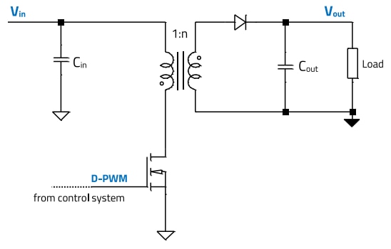
Figure 1: Flyback converter power stage (simplified)
02. BASICS OF FEEDBACK LOOP STABILITY OF SWITCHING POWER SUPPLIES
A flyback converter with its control loop is shown in Figure 2, with the transfer functions expressed in the Laplace s-domain. The plant of the system, with transfer function H(s) (a.k.a. control-to-output transfer function), is formed by the power stage (P(s)) and the duty-cycle generator block (G(s)). Note that the transfer function G(s) will vary depending on the control technique used, producing different plant characteristics for current-mode and voltage-mode control, for example, whereas the power stage transfer function P(s) is independent of the control technique. In Figure 2, a simplified duty-cycle generator block for a peak current-mode controller is shown, as it will be used in the design example of this document. Regarding the compensator, a Type 2 configuration with OP-AMP and optocoupler is illustrated. Such Type 2 compensator can be implemented with different circuits, the most common being OP-AMP (operational amplifier), TL431 (voltage reference with internal error amplifier, as in the design of this application note) and OTA (operational transconductance amplifier).
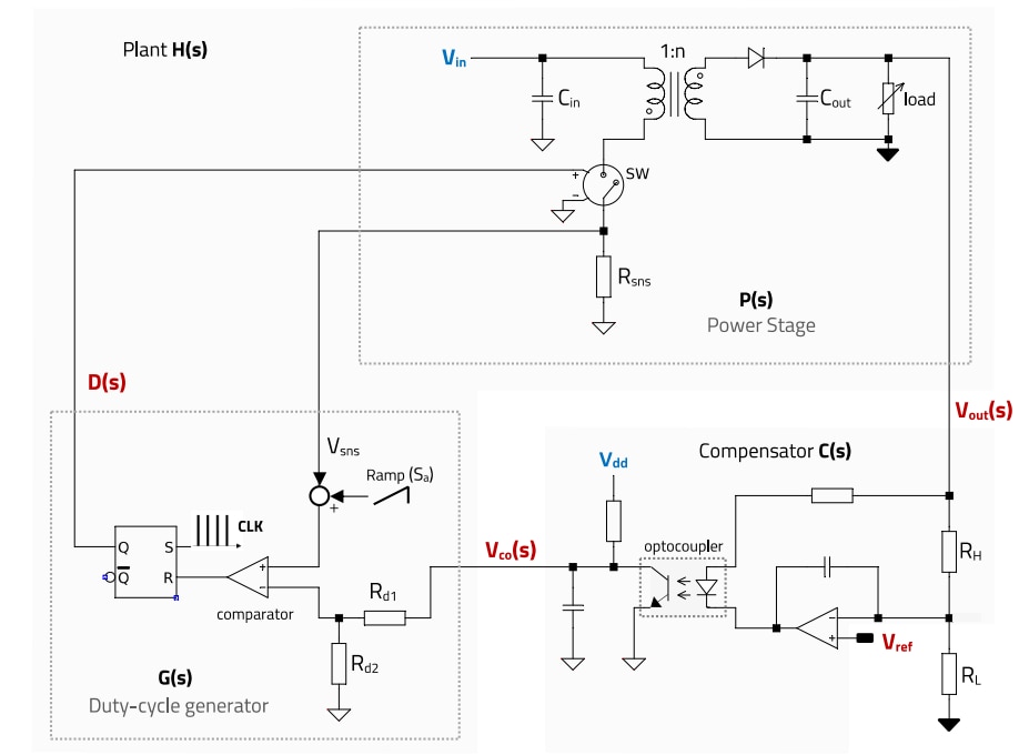
Figure 2: Example of Isolated peak current-mode control Flyback converter with optocoupler and OP-AMP compensator feedback (simplified).
The blocks in Figure 2 form the closed-loop feedback system of Figure 3:

Figure 3: Feedback Loop Block Diagram (unity-gain form)
Note in Figure 2 that the output voltage is reduced by a factor ‘K’ by the resistor divider formed by RH and RL, in order to scale it down for direct comparison to the reference voltage (Vref) at the input of the error amplifier, with:
 (1)
(1)
Applying transfer function block theory, the closed-loop transfer function for DC (s = 0) is:
 (2)
(2)
The resistor divider factor ‘K’ only appears in the DC analysis. In a negative feedback system, the inverting input of the OP-AMP is held to the same DC voltage as the non-inverting input (Vref) if a low-enough impedance exists between the output and the negative terminal of the device. In such case, the resistor RL is effectively connected across two DC nodes, which are the same node for AC: an ‘AC virtual ground’. The closed-loop transfer function for AC is:
 (3)
(3)
In the above, the product of transfer functions of the compensator and plant (i.e. the numerator) forms the open-loop transfer function Gol (s):
 (4)
(4)
From a strict theoretical definition, a stable closed-loop system is one which does not sustain oscillations. Based on the system of E.3, a condition for sustained oscillations is given by the Barkhausen criteria, as follows:
 (5)
(5)
Expressed otherwise:
 (6)
(6)
This condition applied to the open-loop transfer function Gol(s) is translated to the following requirements for its modulus and phase:
 (7)
(7)
 (8)
(8)
Considering s = j ω = j 2 π f, the frequency fc at which E.7 condition is met is known as the crossover frequency (|Gol (fc )|=0 dB). Since Laplace s-domain analysis refers to sinusoidal signals, considering a sinusoidal perturbation in the system, the conditions in E.7 and E.8 mean that if the phase shift provided by the open-loop transfer function at the crossover frequency is -180°, then the system will sustain oscillation at fc, and will therefore be unstable.

Figure 4: Example sinusoidal perturbation propagating around the feedback loop
Figure 4 shows intuitively this concept. A sinusoidal perturbation arising at point ‘a’ in the loop, will become phase shifted - 180° by the negative feedback (i.e. inverting action) of the error amplifier. If it suffers a further -180° phase shift as it passes through the compensator and plant, which form the open-loop transfer function, it will return exactly in phase at the origin point. If the gain provided by the open-loop transfer function is exactly ‘1’, the perturbation will return with the same amplitude, generating a sustained oscillation.
Phase margin (PM)
The phase margin is an indication of how much phase shift a sinusoidal signal of frequency equal to fc would need to undergo to make the system unstable. Based on the diagram of figure 4, it corresponds to the difference between the phase of the openloop transfer function at the crossover frequency (0 dB) and -180°:
 (9)
(9)
Note that the conditions previously shown on E.7 and E.8 only refer to sustained oscillations. However, if the phase margin is too low, although the system is considered ‘stable’ from a theoretical point of view, the output voltage response to a transient event will present oscillations whose amplitude will decay with time (a.k.a. ringing). This may not be acceptable to many systems having to meet stringent specifications regarding overshoot, undershoot and settling time. Figure 5 shows an example transient response of a closed-loop system with a fixed crossover frequency (3 kHz) but different phase margins: PM = 30°, 45°, 60° and 75°. It is observed how, as the phase margin increases, the system response presents less ringing. How much phase margin to select depends on the target transient response, but a worst-case phase margin higher than 45° should be ensured. Note also that a faster settling time can also be achieved by increasing the open-loop crossover frequency.
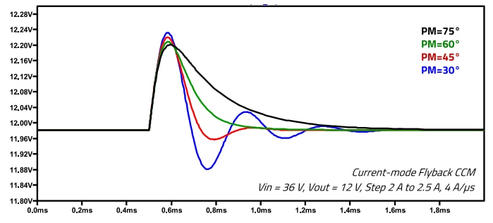
Figure 5: Example transient response for fc = 3 kHz and various phase margin values (LTspice simulation)
Gain Margin (GM)
The gain margin indicates how much gain the system can tolerate before becoming unstable, and it is relevant when considering tolerances of component values or the effect of an underdamped double pole in current-mode control systems. Based again on figure 4, it corresponds to the magnitude of the open-loop transfer function at the frequency where its phase reaches -180° (fgm).
 (10)
(10)
Note that a gain margin higher than 10 dB should be targeted as a general rule-of-thumb [3] .
Compensator Specification
Since the transfer function of the power stage and duty-cycle generator are mostly fixed by the converter design specification and control technique used, a ‘compensator’ circuit is necessary to set the target open-loop crossover frequency and phase margin.
The compensator block will need to provide the gain or attenuation required to make the open-loop transfer function to cross over at the target fc, and will also need to provide the required phase boost at the crossover frequency in order to meet the phase margin specification, while ensuring enough gain margin. Expressing this mathematically:
 (11)
(11)
 (12)
(12)
It is important to note that in the LTspice and MATLAB
plots shown in this document, the phase range used is between - 180° and +180°. In this format, +360° would be added to any phase values between -180° and -360° (e.g. a phase of -250° will appear represented as +110°). In addition to this, the inverting action of the error amplifier (-180°) is already included in the plotted compensator phase curve, since the compensator circuit is built around the error amplifier. Taking into account this format, the phase margin will be directly read as the open-loop phase at fc, and the gain margin as the open-loop gain at the frequency where its phase crosses 0°. In order to understand equation 12, the permanent phase provided by the compensator must be observed. This is formed by the origin pole used to minimize the DC error of the system (integrator action), providing a constant phase of -90°, plus the -180° of the inverting action of the error amplifier. The compensator permanent phase lead is then -270° (i.e. +90°). To this value, the compensator phase boost φcomp_boost is added to form the total compensator phase.
Figure 6 shows the transfer function plots of the plant (V(out), red, cursor 1), compensator (V(ol)/V(out), green, cursor 2/cursor 1) and the resulting open-loop response (V(ol), black, cursor 2)) of an example design like the one presented in this document, as simulated in LTspice. Note that solid lines correspond to the magnitude (dB) (left axis), whereas dotted lines to the phase (deg) (right axis) of the corresponding transfer function. In this example, the plant shows a gain of -1.41 dB at fc = 2.88 kHz and - 80.7° phase. The compensator provides a gain of +1.41 dB and a phase boost of around 60° at ‘fc’ (151.5° - 90°). As a result, the open loop transfer function crosses 0 dB at 2.88 kHz with a phase margin of 151.5° - 80.7≃70°, and the gain margin is around 20 dB. This is an example of a stable feedback loop design.
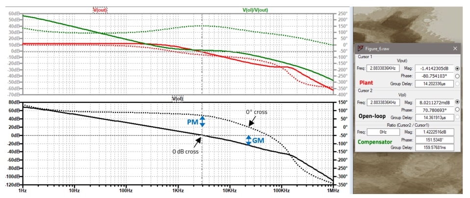
Figure 6: Example of plant, compensator and open-loop transfer function Bode plots showing (fc), PM and GM (LTspice Simulation)
03. THE PLANT (CONTROL-TO-OUTPUT) TRANSFER FUNCTION OF A CURRENT-MODE FLYBACK CONVERTER
Once the design of the converter power stage is completed, the first step in the compensation procedure is to study the characteristics of the plant transfer function formed by the power stage and the duty-cycle generator. Note that the plant transfer function will be different depending on whether the converter operates in continuous conduction mode (CCM) or in discontinuous conduction mode (DCM), so both conditions need to be considered.
For the analysis, the design specifications used are the following, based on the design prototype presented later in section 010:

For the above specification, the converter will enter DCM operation for an output current of around 1.25 A.
The transformer used in the design is the WE-PoEH 7491195112 [8] from Würth Elektronik and the IC controller the NCP12700 from onsemi [9]. This IC integrates the simplified duty-cycle generator block shown in previous figure 2, in addition to many other relevant safety and functional features. It is observed that the compensator output voltage Vco is divided by resistors Rd1 and Rd2, before being fed to the peak current setting comparator (fig. 2). In the case of the NCP12700, the divider factor is Vdiv=6 (i.e. Rd1=5∙Rd2). This means that the magnitude of the plant transfer function is also divided by ‘6’ in this case, as the resistor divider is like a simple gain block in the feedback path. Since at the highest power demand (highest magnetizing peak current) V(co_max) ≈ Vdd, which is typically around 5 V (see [9]), , the resistor divider will produce in this case a voltage V(co_div) = 833 mV at the comparator input. Such low voltage allows to select a lower value of the current sense resistor for the same peak current setting, improving with it efficiency, while still allowing the compensator output voltage to keep a wide dynamic range (0.2 to 5 V).
Regarding the added compensation ramp (Sa), it is generated internally by the NCP12700 and it is variable, meaning that its slope is adjusted depending on the switching frequency and duty-cycle. A table of values is provided as a reference in the datasheet. For Fsw ≈ 300 kHz as in this design, the generated compensation slope is found in the range between 33 kV/s and 81 kV/s.
3.1 Continuous Conduction Mode Operation (CCM)
The plant transfer function of a current-mode flyback converter operating in CCM is of the form [1]:
 (13)
(13)
It features a DC-gain (Go), a zero (ωz), a right-half plane zero (ωrhpz), a pole (ωp) and a double-pole at half of the switching frequency (ωn), which models the subharmonic oscillation instability as the duty-cycle approaches and exceeds 50% in a peak current-mode converter.
Prior to selecting a crossover frequency and to design the compensator, it is necessary to plot the magnitude and phase versus frequency of the plant transfer function (i.e. Bode plot). This can be done in different ways: from an analytical small-signal model of the converter [1], via a SPICE simulation with an averaged PWM switch model [2], or measuring it directly if a prototype is available.
Figure 7 shows the plant transfer function characteristic for the design specification above, albeit without slope compensation ramp applied (Sa = 0). The results are based on the analytical model provided in [1], and plotted using MATLAB. Considering E.13, the following values are obtained for minimum input voltage (36 V) and full load (2.5 A):

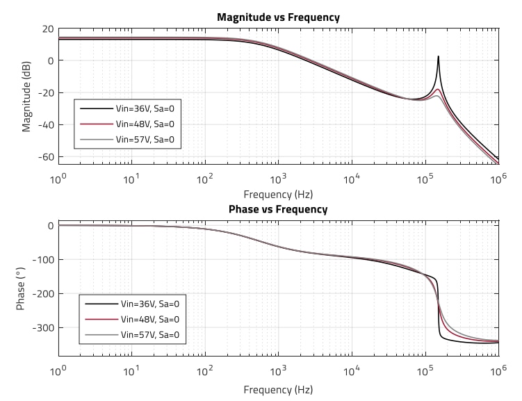
Figure 7: Plant transfer function in CCM operation for Vin range (36 V, 48 V, 57 V) and Sa = 0 (MATLAB)
The magnitude curve presents a 1st order characteristic in the lower frequency range. Note that the zero formed by the output capacitor and its ESR (ωz) happens at a very high frequency, and it is therefore out of the range of interest. This is due to the extremely low ESR value (out of paralleling 12 x MLCC WCAP-CSGP-885012109010). This means that special considerations regarding ESR variations are not necessary, but any beneficial phase boost provided by this zero in the lower frequency range is lost. Although in this design the right-half-plane zero also happens at a relatively high frequency, it starts to contribute phase lag at around one decade before, and it is typically the main constraint in selecting the crossover frequency.
It is observed how the double-pole causes a dramatic phase drop at fn = fsw/2. At minimum input voltage (D = 49%) and without compensation ramp the quality factor (Qp) is very high, 17.1, signaling instability with the high peaking of the plant transfer function magnitude at fn. For nominal and maximum input voltages, the duty-cycle is 42% and 38%, respectively, with a quality factor of 3.56 and 2.44, and a much lower peaking is observed. Excessive peaking degrades the gain margin and can make the system unstable when causing the magnitude of the open-loop transfer function to cross over 0 dB more than once, complicating stability analysis.
Some compensation ramp is therefore necessary to ‘damp’ the peaking. The minimum value of compensation ramp required to ensure stability at all duty-cycles is:

 (14)
(14)
where S2 is the magnetizing current slope during the off-time of the power inductor/transformer, as sensed through the sensed resistor Rs, with units of kV/s:
 (15)
(15)
The transformer turns-ratio ‘n’ is 0.374 and the above expression yields Sa ≥ 61 kV/s. It should be noted, however, that the converter does not need ramp compensation for all duty-cycles. Since Dmax = 0.49, a lower slope compensation will suffice. This is confirmed by plotting the plant transfer function for Sa= 30 kV/s and Sa = 80 kV/s, as shown in Figure 8 and Figure 9. The peaking is well damped even at the minimum expected compensation ramp.
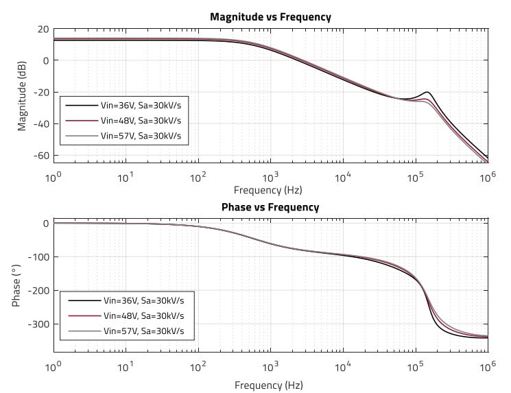
Figure 8: Plant transfer function in CCM operation for Vin range (36 V, 48 V, 57 V) and Sa = 30 kV/s (MATLAB)
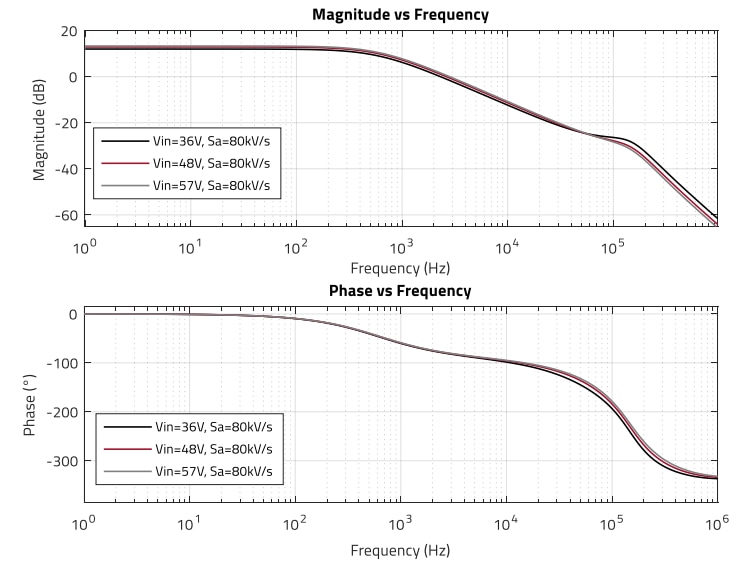
Figure 9: Plant transfer function in CCM operation for Vin range (36 V, 48 V, 57 V) and Sa = 80 kV/s (MATLAB)
3.2 Discontinuous Conduction Mode Operation (DCM)
The control-to-output transfer function of a current-mode flyback converter operating in DCM is of the form [1]:
 (16)
(16)
As observed, in DCM there is no subharmonic oscillation instability and therefore no double-pole in the model. There is a righthalf-plane zero but it happens at a higher frequency than in CCM. The same applies to the additional second pole and the ESR zero. For this reason, in the low-frequency range the current-mode flyback converter in DCM can be approximated by a single pole system, dominated by ωp1, where:
 (17)
(17)
As the output current reduces, the pole moves to a lower frequency. The values in this case, for Vin = 36 V, Iout= 0.8 A and Sa= 0 are:

Figure 10 shows the Bode plot of the DCM plant transfer function for input voltages of 36 V, 48 V and 57 V, and 0.8 A output current:
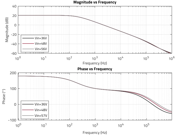
Figure 10: Plant transfer function in DCM operation for Vin range (36 V, 48 V, 57 V) and Sa = 0 kV/s (MATLAB)
In previous Figure 7 to Figure 10 a common feature of current-mode control is clearly observed: the frequency response does not depend (almost) on the input voltage. Any input voltage variation will directly affect the slope of the magnetizing current. For a specific current peak setpoint, this will in turn change the duty cycle allowing for more or less energy transfer to the secondary side to keep the output power constant, without the need of causing an overshoot or drop of the output voltage to make the control loop react. This inherent feed-forward functionality is one of the main advantages of the current-mode control technique.
04. COMPENSATOR REQUIREMENTS
As seen in previous section, CCM operation presents higher requirements for compensation than DCM. Therefore, the compensator is typically designed for CCM at worst-case operating conditions (i.e. minimum input voltage and full load current), checking also the behavior for DCM to ensure it is still acceptable, and performing any necessary adjustments to obtain the required performance in both cases.
The target crossover frequency of the open-loop transfer function is selected to be anywhere below 1/5th of the switching frequency (for switching frequency noise attenuation), or 1/5th of the minimum right-half-plane zero frequency, whichever is lower. In many cases, the right-half-plane zero becomes the limiting factor, as in this design example. Note that the above is simply a rule-of-thumb for a very stable design, but different margins can also be used at the discretion and preference of every designer. In this case:
 (18)
(18)
 (19)
(19)
 (20)
(20)
The crossover frequency should then be set lower than 14 kHz. The frequency area of interest for compensation is highlighted in Figure 11:
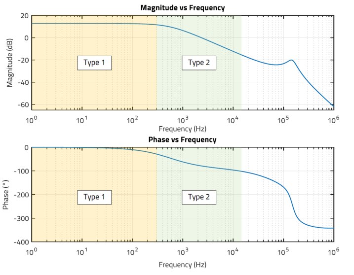
Figure 11: Frequency range of interest for crossover frequency selection and suitable compensator type
In the frequency range of interest (below 14 kHz), the plant shows a 1st order characteristic after the dominant pole of the system even in CCM operation (green) (slope of -20 dB/dec). In this area a Type 2 compensator is typically used, as it can provide the required gain and a phase boost up to 90°. If the crossover frequency is selected below the dominant pole (yellow), a simple Type 1 compensator (integrator-only) can be used to just provide high DC gain to minimize the static DC-error without any phase boost. It is observed that at such low frequency range the plant’s phase shift is nearly zero, reaching -45° at the frequency of the dominant pole, and a phase margin from 45° to 90° can then be achieved with a simple Type 1 compensator.
It must be noted however that a lower crossover frequency has the drawback of a lower closed-loop bandwidth, which in turn causes a slower reaction of the closed loop system to changes in the output voltage, leading to higher overshoot, undershoot and settling time. Therefore, a compromise between transient performance and high-frequency noise attenuation needs to be found when selecting the crossover frequency. Note that adding more output capacitance can also help to improve the transient characteristic despite a low crossover frequency, albeit with the added cost.
In this case, a target crossover frequency of fc = 10 kHz is (initially) selected, with a target phase margin of PM = 70°. The magnitude and phase of the control-to-output transfer function at fc are shown in Figure 12:
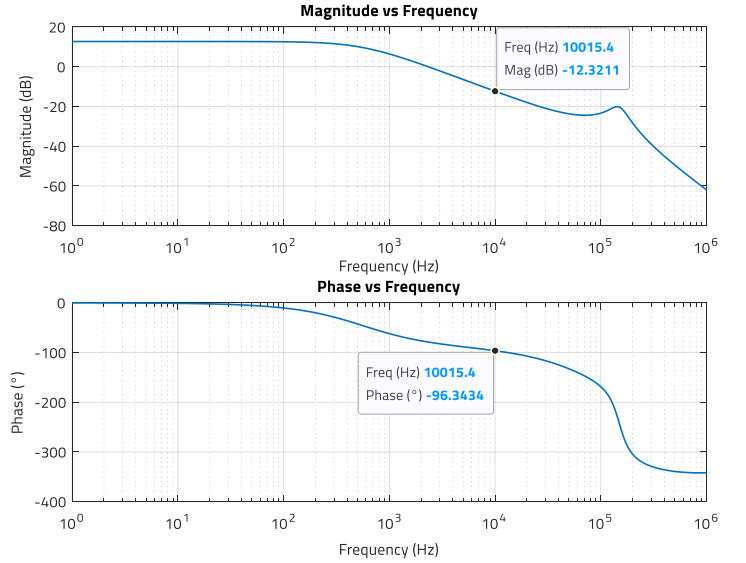
Figure 12: Magnitude (dB) and Phase (deg) of plant transfer function at fc = 10 kHz (MATLAB)
With a Type 2 compensator, the maximum phase margin achievable in this case is 83.6°, which is enough for the 70° target. The compensator needs to provide a gain of +12.3 dB (equivalent to 4.12 unitless), to offset the plant gain and make the magnitude of the open-loop transfer function to cross over at fc =10 kHz:

With a target phase margin of 70°, the phase boost that the compensator needs to provide at fc is:

05. DESIGN OF A TYPE 2 COMPENSATOR WITH TL431 AND WL-OCPT OPTOCOUPLER
With the compensator requirements set, a Type 2 compensator circuit needs to be selected. A very popular configuration for an isolated current-mode Flyback converter is based on the TL431 voltage reference and an optocoupler as shown in figure 13. This solution is widely used due to its low-cost, simple design and good enough performance.
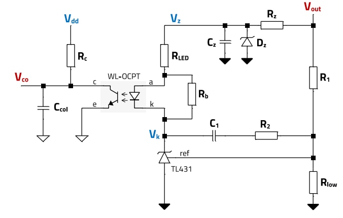
Figure 13: Type-2 compensator circuit with TL431 and WL-OCPT optocoupler
5.1 Circuit Operation
In Figure 13, it is observed that the optocoupler is biased in a common-emitter configuration, and so as the current through the LED increases, the collector-emitter voltage (Vco) decreases. Note that, based on previous Figure 2, Vco sets the magnetizing peak current and this way, indirectly, also the amount of energy transferred to the output. The TL431 sets the current through the LED by adjusting its cathode voltage (Vk), based on the output voltage (Vout). The TL431 acts like an error amplifier, and its internal structure is shown in figure 14 (based on the datasheet [10]).
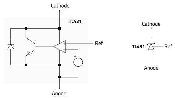
Figure 14: TL431 internal circuit [10]
When the voltage in the ‘Ref’ terminal is higher than the internal fixed reference voltage of the TL431, caused for example by an output voltage overshoot due to a sudden reduction in the load current, then more current is fed into the base of the npn transistor, and the cathode voltage of the TL431 decreases (change in operating point of the npn transistor within active region). This causes a higher voltage across RLED and the optocoupler LED, with the subsequent increase in the LED current and, in turn, in the collector current. A higher collector current causes a higher voltage drop across Rc, resulting in a lower collectoremitter voltage, which in this configuration, represents the compensator output voltage (Vco). A lower Vco sets a lower peak current setpoint, reducing the magnetizing current amplitude and, with it, reducing the amount of energy transferred to the secondary side. The output voltage is then brought back to the target regulated level. The opposite happens when there is a sudden increase in load current. Figure 15 illustrates this principle of operation for both, high-to-low and low-to-high load current steps (2.5 A to 2 A), for the specifications of this design.
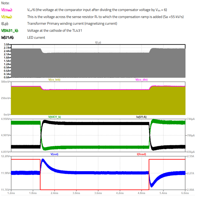
Figure 15: Example transient waveforms of the Type 2 compensator with TL431 and WL-OCPT optocoupler (LTspice)
5.2 DC-Biasing the TL431 and WL-OCPT Optocoupler
For the compensator circuit to operate as described, the TL431 and optocoupler need to be DC-biased correctly. Specifically, the internal npn transistor of the TL431 and the output phototransistor of the optocoupler need to be biased in their active region for dynamic performance, and stay so even after any expected variations and tolerances of parameters are factored in. For the optocoupler circuit, Rc= 5 kΩ and Vdd = 5 V are internally set in the NCP12700 controller [9] .
Regarding the TL431 device [10], it requires a minimum cathode bias current of 1 mA and the minimum cathode voltage equals the reference voltage, in this case, 2.5 V.
The LED of the WL-OCPT 817 series has a worst-case minimum forward voltage drop of 0.85 V at 0.1 mA and 110°C (Figure 16). Adding a resistor (Rb) in parallel with the LED is a common technique used to generate a mostly constant current source for the TL431, since in normal operation there is always current flowing through the LED, and the voltage applied across Rb will be the forward voltage drop of the LED (Vf). Considering a minimum TL431 bias current of Ib_TL431_min=2 mA, the maximum allowable resistor value is:
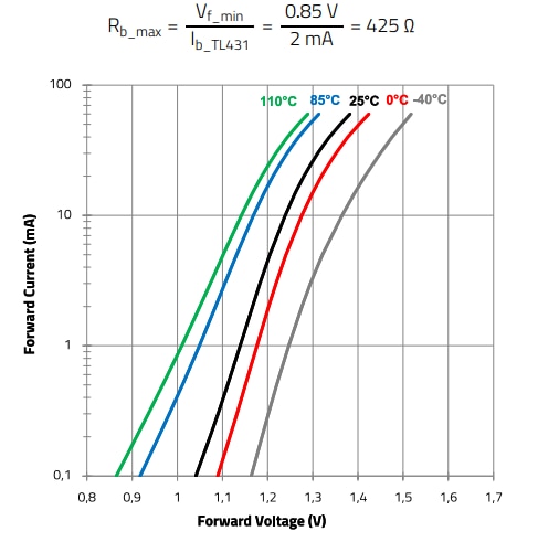
Figure 16: WL-OCPT 817 series - LED forward voltage vs forward current curve as a function of ambient temperature
Regarding the minimum TL431 bias voltage (Vk_min), we have:
 (22)
(22)
The maximum voltage drop across the LED resistor (VR_LED_max) happens at the maximum LED current (ILED_max), which in turn happens when the collector voltage is lowest (Vce_min = Vce_sat = 0.2 V). This in turn implies maximum collector current at the minimum absolute CTR, as follows:
 (23)
(23)
The value of the LED resistor needs to be lower than:
 (24)
(24)
To calculate RLED_max, it is necessary first to estimate the minimum CTR value of the WL-OCPT optocoupler. An example procedure for this is presented next.
Estimating minimum CTR of WL-OCPT optocoupler
The optocoupler CTR is affected by wide variations caused not only by technology and manufacturing tolerances but also by its dependence upon parameters like LED current, ambient temperature and operating time.
In order to reduce the CTR range to consider for a specific design, the WL-OCPT optocoupler series are classified in ‘binnings’, each of which guarantees a CTR value within a certain range for a specific DC-Bias condition, as the table in Figure 17 shows.

Figure 17: Example of WL-OCPT optocoupler CTR binning for 817 and 816 series
Choosing a device from the ‘A’ binning means the CTR will range from 0.8 to 1.6 out of the production line. However, this is valid only for an LED current of 5 mA and a collector-emitter voltage of 5 V. For different specifications, the CTR range needs to be recalculated. The absolute CTR curve provided in the WL-OCPT datasheet for all binnings shows this dependence (Figure 18).
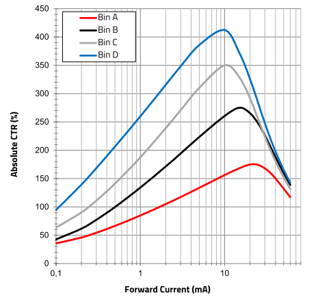
Figure 18: WL-OCPT 817 Series: Absolute CTR vs. LED forward current (at Vce = 5 V)
For more detailed information on the basics of optocouplers, please see Application Note on reference [12] . The DC bias conditions of the optocoupler at the operating point of interest must be known in order to estimate the minimum CTR. In the feedback loop, the collector-emitter voltage Vco is divided by a factor Vdiv before being fed to the current peak comparator (Vdiv = 6 V for the NCP12700). The control voltage Vco provided by the compensator in a CCM current-mode converter controls the primary peak current setpoint, and thus its level depends on the converter output power. For full-load, the control voltage will be at the maximum value, and as the load reduces, the control voltage will be lower. Note that the CTR varies slightly with Vce.
The following expression can be used to estimate the control voltage fed to the comparator in a peak current-mode Flyback converter:
 (25)
(25)
Taking Vin(nom) =48 V, Sa = 55 kV/s, (middle of the range of Sa = 33 kV/s to 80 kV/s) and full load Iout = 2.5 A, it is obtained:

This generates a steady-state collector current of:
 (26)
(26)
A WL-OCPT optocoupler from binning A is selected for the design, and the resulting CTR under this bias condition can be measured experimentally using the setup shown in Appendix A. Alternatively, it can be obtained with the LTspice simulation fixture shown in Figure 19, thanks to individual SPICE models provided by Würth Elektronik for each binning of the WL-OCPT 817 optocoupler series. In this case, for Vce = 2.7 V, the CTR is 0.71, with an LED current of 0.65 mA and a collector current of 0.46 mA.
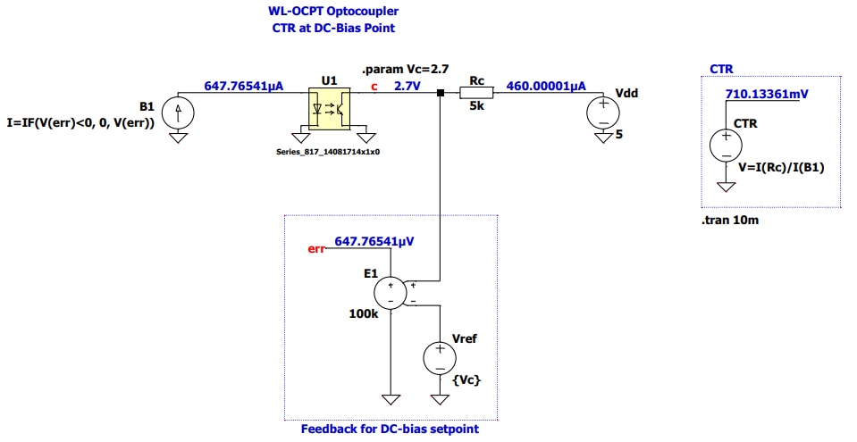
Figure 19: SPICE simulation for obtaining CTR with SPICE model of WL-OCPT 817 A (LTspice)
Note that these SPICE models consider a CTR near the average of the tolerance range of the respective binning at DC-bias conditions of Vce = 5 V and IF = 5 mA (in this case for binning ‘A’ this is CTRn ≈1.2). The relative CTR for this DC-bias condition is:

Since the CTR only changes slightly with collector-emitter voltage (as long as the phototransistor stays in the active region of operation), a similar CTR value of 1.2 for Vce = 5 V and Vce = 2.7 V at IF = 5 mA can be approximated. Figure 20 shows that the relative CTR vs LED current curves for different binnings do not differ notably below an LED current of 5 mA, however, as the optocoupler phototransistor starts to operate close to the saturation region (Vce below 0.5 V), more difference in the curves will be observed. With this, based on Figure 20, an LED current of 0.65 mA would correspond to a relative CTR of around 0.55 considering a device from bin A. Relative CTR curves help to estimate the absolute CTR of a device when its CTR value at the test DC-bias conditions deviates considerably from the average value of the binning.
To the obtained absolute CTR value of 0.71, the production tolerance spread of the binning ‘A’ must be added. A minimum and maximum CTR of 0.8 and 1.6 corresponds to a deviation of ±30% from the average CTR of 1.2. The range in this design is then:

Note that the relative CTR curve in previous Figure 18 considers an operating temperature of 25°C, but the CTR also varies with ambient temperature as shown in Figure 21. Considering a temperature range of -20°C to 85°C, the minimum CTR value calculated above must be multiplied by a factor of 0.85 (@Ta = 85°C), and the maximum by a factor of 1 (@Ta= 10 to 30°C), obtaining the new CTR range:


The minimum CTR value at start-of-life is in this case:
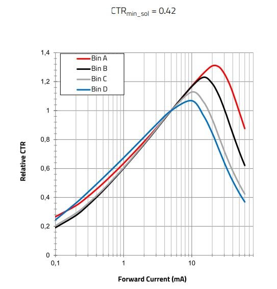
Figure 20: WL-OCPT 817 Series: Relative CTR vs. LED forward current (at Vce = 5 V)
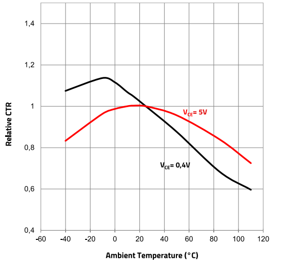
Figure 21: WL-OCPT 817 series - Relative CTR vs. Ambient Temperature curve
Minimum CTR at end-of-life
The optocoupler CTR also reduces with operating time. This is caused mainly by degradation of the LED with the corresponding reduction in emission efficiency, as the LED generates fewer photons for the same forward current. The rate of degradation is directly proportional to the LED operating temperature, and in turn, to the LED forward current. The Application Note in reference [13] provides guidance to estimate the expected CTR reduction for a set operating condition. In this design, considering a maximum temperature of 80°C and LED current of 0.65 mA, based on the test curves [13], for 20 years’ operating time the CTR would degrade less than 5%. This however considers an LED current of 5 mA, which is much higher than the maximum in this design (0.2 mA ≤ ILED ≤ 0.42 mA). Although the CTR degradation for this design specification can be neglected, for the sake of the example, a degradation of 5% is considered:

An absolute minimum current transfer ratio of CTRmin = 0.35 is considered, adding some extra margin.
LED resistor calculation
From previous E.24, considering Vz = 9 V (see next for details), Vce_sat= 0.2 V [11] and Vf = 0.81 V, it is obtained:

A slightly lower standard value of 1 kΩ is selected.

Note that the resistor value does not have any influence on the LED current, which is set only by the collector current and the CTR when the converter is operating in closed-loop, since the collector-emitter voltage is set by the required duty-cycle, which in turn is set by the input voltage and load current.
The AC decoupling Zener supply
The components Rz, Dz and Cz form a simple Zener regulated supply, whose main function is to provide a DC voltage to the LED anode which is AC-decoupled from the converter output voltage. This way, it is ensured that the LED current is only AC-modulated by the TL431 cathode voltage. Otherwise, the LED current would also become AC-modulated by the output voltage variations itself, which would place further constraints in choosing the LED resistor value (see [3] for more details). The Zener voltage needs to be chosen high enough to provide a wide dynamic range to control the LED current and reduce power dissipation in Rz, but at the same time low enough to keep power dissipation in the Zener diode low. A Zener voltage of 70 to 80% of the output voltage (Vout=12 V) is considered in this case as a good compromise:
 (28)
(28)
A device with standard voltage Vz = 9.1 V is selected.
The maximum value of the Zener resistor (Rz) is limited by the maximum current across the LED resistor plus the bias current of the Zener diode (Ib_Zener), selected in this case as 2 mA in order to reduce its impedance and improve with its AC filtering, as follows:
 (29)
(29)
A standard value of 470 Ω is selected. The power dissipation in the resistor is:
 (30)
(30)
The maximum power dissipation in the Zener diode happens when the LED current is zero:
 (31)
(31)
The resistive divider The resistors R1 and Rlow set the output voltage to the desired value, based on the reference voltage of the TL431. Setting Rlow = 10 kΩ, then:

A value of 38.3 kΩ is selected.
5.3 Compensator components design
For AC-analysis, the compensator circuit from previous Figure 13 can be replaced by the AC schematic of Figure 22.

Figure 22: Equivalent AC circuit for the Type 2 compensator with TL431 and WL-OCPT Optocoupler
In the AC circuit model, the TL431 is modelled like an error amplifier, producing an AC voltage Vka(s) which modulates the LED current. In this regard, the LED dynamic resistor (rd) is also included in the model. Although its value is typically very small, it increases as the LED current reduces, causing a higher portion of the LED current to flow through the bias resistor Rb instead, reducing with it the compensator gain. Note that the capacitance Copto is the parasitic collector-emitter capacitance of the optocoupler phototransistor. The transfer function of a Type 2 compensator like that of figure 13 features a zero (ωz), a pole (ωp), and an origin pole (ωpo):
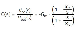 (13)
(13)
Where Gm = ωpo/ωz. From the circuit of Figure 22, the following transfer function expression is obtained:

Considering s = j ω = j 2 π f, it is obtained:
 (35)
(35)
 (36)
(36)
 (37)
(37)
Note that the CTR parameter in the compensator AC circuit model and in the midband gain expression (E.35) corresponds to the small-signal CTR of the optocoupler, which in this case is slightly higher than the DC-CTR value calculated. Note however that the DC-CTR value will still be considered for the following compensator design steps as an approximation. Figure 23 shows the typical frequency response characteristic of a Type 2 compensator. If the zero is located at a lower frequency than the pole, then exactly at a frequency equal to the geometric means of the two frequencies (fg=√(fz∙fp )), the gain equals the midband gain Gm. This is also the frequency of the maximum phase boost of the compensator. The further apart the pole and zero are, the higher the phase boost provided, up to a maximum of 90°. Based on this, if the pole-zero geometric means frequency is set at the target crossover frequency of the open-loop transfer function (fg= fc), then the midband gain of the compensator can be simply set to offset the gain of the plant at fc, and the zero and pole frequencies are placed symmetrical to fc and far enough apart to provide the phase boost necessary to meet the phase margin specification. This compensation procedure is known as ‘k-factor’ [3][4] .
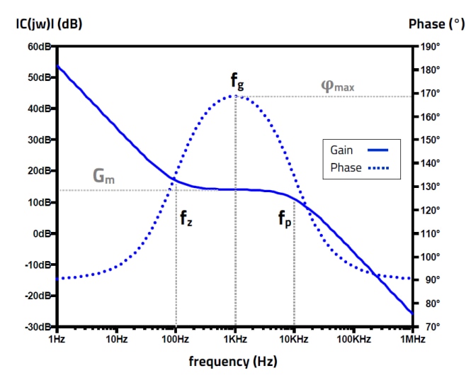
Figure 23: Type-2 compensator: Frequency response example (LTspice simulation)
In this compensator circuit, the midband gain directly depends on the CTR (E.35), so we can advance that any CTR variations will cause a change in the midband gain and in turn, a shift in the crossover frequency of the open-loop transfer function, from which additionally the phase margin will be affected. This shows the importance of knowing not only the minimum CTR, but also the full range of CTR variation. Note that the small-signal CTR follows the variations of the DC-CTR over the full current range of this application (below 1 mA). It is also observed that the collector-emitter parasitic capacitance of the optocoupler phototransistor (Copto) sets the pole frequency of the compensator, together with any added capacitance (Ccol).
From previous section 4, the compensator specification is recalled as:
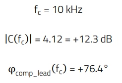
Since values of CTR, Rc, RLED and R1 are already set for DC-biasing purposes, R2 is calculated to set the required midband gain:
 (38)
(38)
A standard value of R2 = 44.2 kΩ is selected.
To obtain a phase lead of +76° at 10 kHz, the zero and the pole frequencies are calculated as follows [3]:
 (39)
(39)
 (40)
(40)
which yields fp= 83.25 kHz and fz =1.2 kHz.
The capacitor C1 is calculated from previous E.36 to set the zero at the required frequency:

A standard value of C1 =3.3 nF is selected, with a zero frequency slightly lower at fz ≈ 1.1 kHz.
The capacitance at the compensator output necessary to set the pole frequency is (E.37):

with:

It is observed that, if the optocoupler parasitic capacitance is higher than 0.38 nF in this case, then the pole cannot be set at the target frequency of 83.25 kHz.
06. OPTOCOUPLER POLE LIMITATION AND SOLUTIONS
The collector-emitter parasitic capacitance of the optocoupler (Copto) and in turn the pole frequency varies slightly with the collector-emitter voltage (Vce). The lower the collector-emitter voltage, the lower the pole frequency (due to higher Copto). For this design, taking Vce= 2.7 V as calculated before for full-load condition, the pole frequency of the WL-OCPT 140817140110 device has been measured with the setup shown in Appendix B. Figure 24 shows results of one of the samples measured. Out of a total of 20 units, the measured pole frequency was found between 24.2 and 25 kHz. Taking fp = 24.6 kHz in the middle of the range, this corresponds to a parasitic capacitance of:
 (41)
(41)
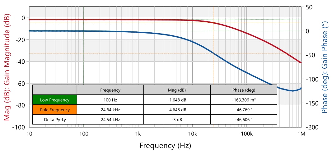
Figure 24: Measurement result for WL-OCPT 817 Bin A pole frequency (Bode100)
Measurements were also made for Vce = 2 V, resulting in a slightly lower pole frequency in the range of 22.9 to 23.7 kHz. Note that if a WL-OCPT device from another binning with higher CTR were selected (e.g. Bin ‘B’ or ‘C’), the optocoupler pole frequency will be lower. For the same DC-Bias conditions as considered here, samples from the Bin ‘B’ showed a pole frequency of around 18 kHz, whereas for the Bin ‘C’, it was around 12.5 kHz. The reason for this is the mutual dependence of the CTR and Copto. A higher CTR can be achieved, for example, by increasing the base-collector area of the output phototransistor so that to increase its sensitivity to the oncoming photonic energy. This however results in a higher parasitic capacitance and a lower optocoupler pole frequency.
In E.41, it is observed that Copto is higher than the maximum value of 0.38 nF required to set the compensator pole at 83.25 kHz in this design.
6.1 Solution 1: Select a lower crossover frequency
A typical solution to the optocoupler limitation is to reduce the target crossover frequency. However, special attention should be paid to the transient response, since a lower crossover frequency of the open-loop transfer function causes the control loop to react more slowly to transients.
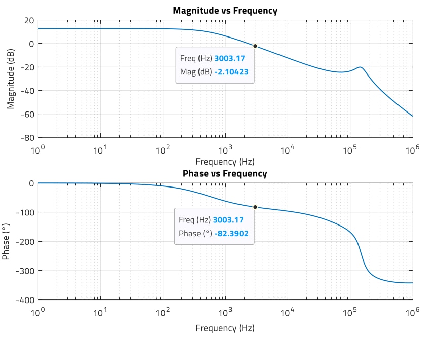
Figure 25: Magnitude (dB) and phase (°) of plant transfer function at fc = 3 kHz with Sa_min = 30 kV/s (MATLAB)
Selecting fc = 3 kHz, from the plant magnitude and phase in Figure 25, the requirements for the compensator are:

The required zero and pole frequencies are recalculated from E.39 and E.40:
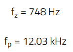
Compensator component values are also recalculated:
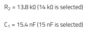
The zero frequency with the selected values is f=758 Hz
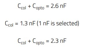
The pole frequency with the selected Ccol value is slightly higher at fp = 13.8 kHz. With these values, the compensator frequency response of Figure 26 is obtained.
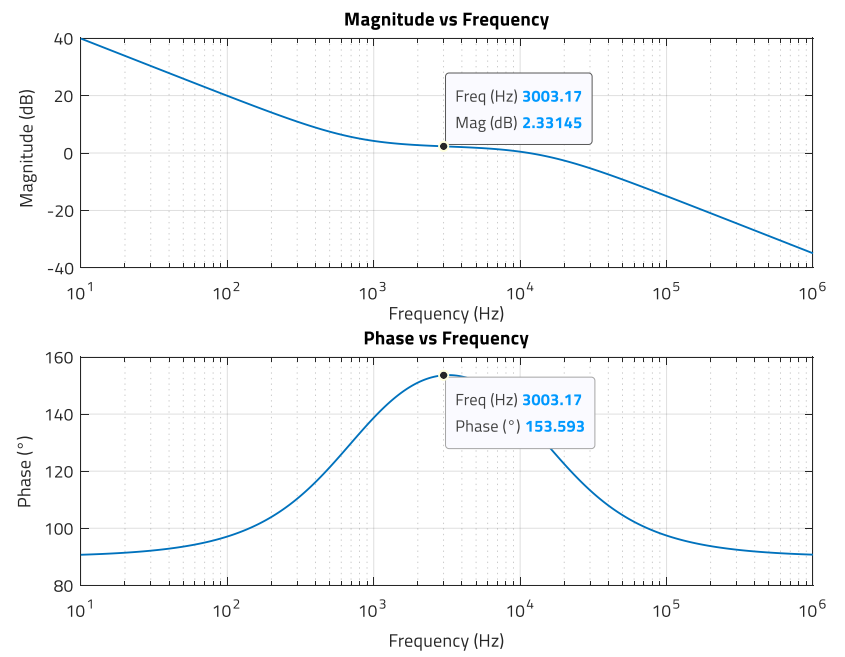
Figure 26: Magnitude (dB) and phase (°) of compensator for solution-1 (MATLAB)
It is observed how at the target fc = 3 kHz, the gain is around 2.3 dB and the phase boost: 153.5° - 90° = 63.5°. These very close but not exact values to the requirement are the result of using standard available values for the components, instead of those theoretically calculated.
6.2 Solution 2: Add a zero to cancel the optocoupler pole. Add a pole for the compensator
If the crossover frequency cannot be reduced, a possible solution is to add both a zero and a pole to the system. The zero will be set at the optocoupler pole frequency to cancel its effect. The pole is set at the target pole frequency of the compensator. With this, the limitation from Copto is eliminated and the target crossover frequency can be achieved. A resistor (R3) and a capacitor (C3) in parallel with R1 create the additional pole and zero, as shown in Figure 27. This configuration corresponds, in fact, to a Type 3 compensator, but since the effects of the added zero and the optocoupler pole mutually cancel each other, the system effectively provides a Type 2 compensator response, with a zero, a pole and a midband gain.
Note that the added zero can compensate the optocoupler pole directly, or an additional capacitance Ccol can be added to shift the pole at a lower frequency range, and then cancel it there. This helps to reduce the impact of the small variations in the optocoupler pole frequency.
Adding Ccol = 3.3 nF, the pole frequency is shifted to (E.37):

The pole is placed at the required frequency previously calculated (E.39) (fp2 = 83.25 kHz), and R3 is calculated to set the zero [3]:

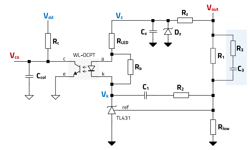
Figure 27: Type 3 compensator configuration with TL431 and WL-OCPT optocoupler
A value R3 = 3.6 kΩ is selected. The capacitor C3 is calculated to set the pole [3]:
 (43)
(43)
A value of C3 = 0.47 nF is selected. With this, the compensator frequency response obtained is:
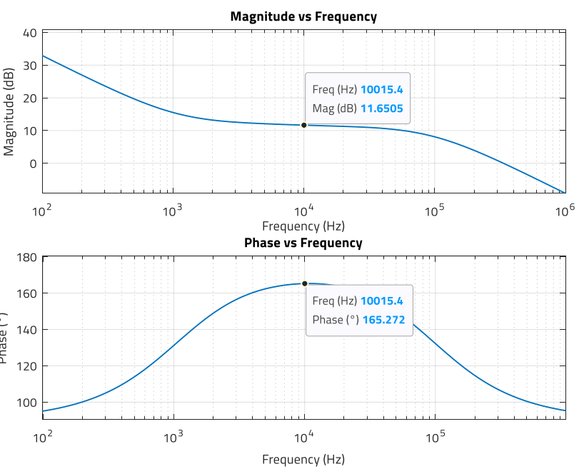
Figure 28: Magnitude (dB) and phase (°) of compensator for solution 2 (MATLAB)
It is observed how at the target fc = 10 kHz, the gain provided is around 11.65 dB and the phase boost: 165.3° - 90° = 75.3°.
07. OPEN-LOOP RESPONSE: PHASE AND GAIN MARGINS
For solution-1 (Figure 29), it is observed a crossover frequency of 3.06 kHz and a phase margin of around 71°. The gain margin is around 25 dB, far higher than the minimum recommended of 6 dB. Regarding solution 2 (Figure 30), it is observed a crossover frequency of around 9.3 kHz and a phase margin of 69.2°, nearly 70°. The gain margin is around 15 dB, showing the importance of damping the resonant double-pole.
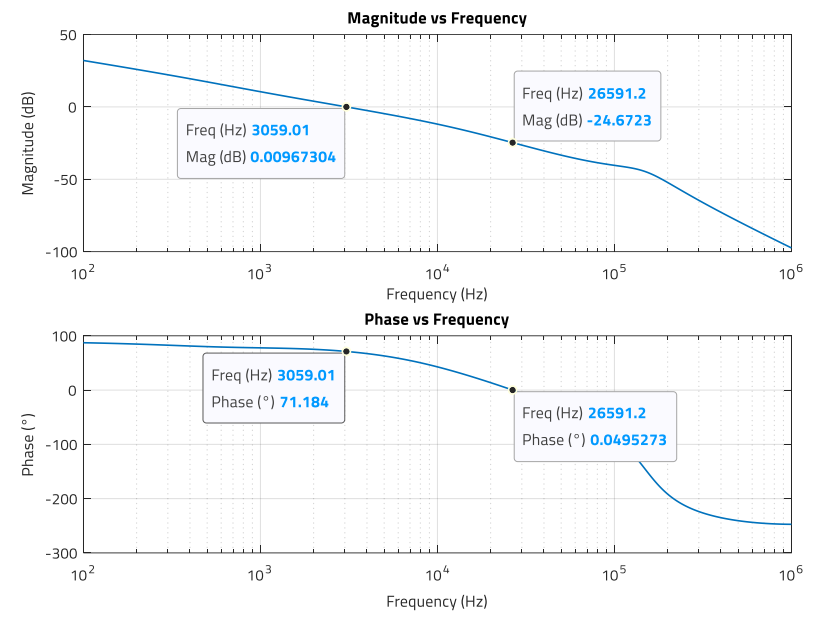
Figure 29: Magnitude (dB) and phase (°) of open-loop transfer function for compensator solution 1 (MATLAB)
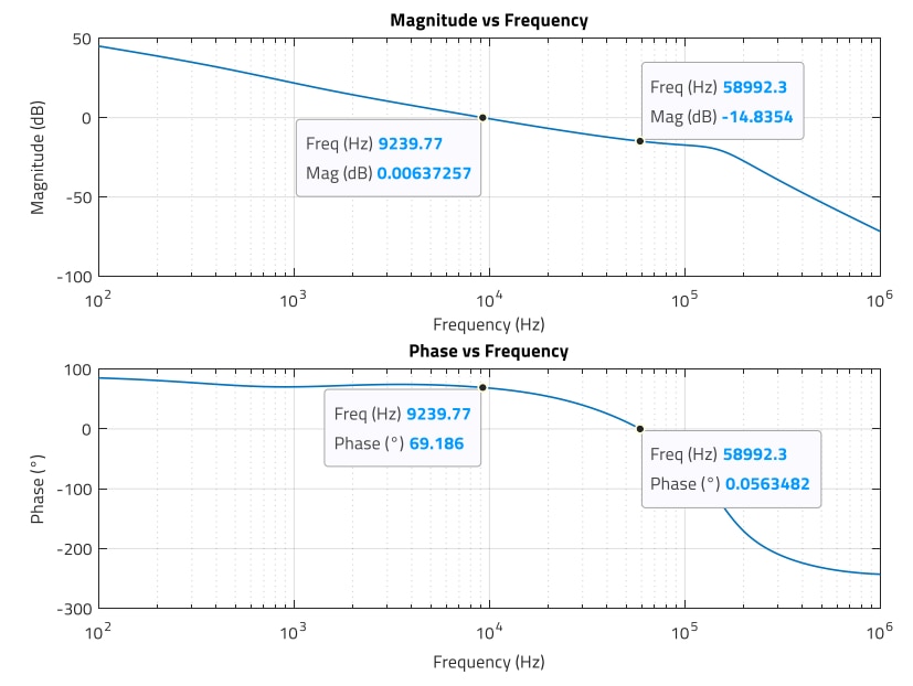
Figure 30: Magnitude (dB) and phase (°) of open-loop transfer function for compensator solution 2 (MATLAB)
08. TRANSIENT RESPONSE COMPARISON
A higher open-loop crossover frequency (solution-2) provides a higher bandwidth for the closed-loop system. A higher bandwidth means that the loop will react faster to correct the output voltage after any transient deviations from the regulated value. This can be appreciated in Figure 31, which compares the transient response of both solutions to a load current step from 2 to 2.5 A with a slew-rate of 1 A/us. Although the transient response is ‘well-behaved’ in both cases without ringing due to the high phase margin of 70°, it is observed how the higher closed-loop bandwidth of solution 2 causes lower overshoot and undershoot as well as shorter settling time due to the faster reaction time. Note that the results were obtained in LTspice with a converter using an averaged PWM switch model as proposed by Christophe Basso in [2] (this is the reason for not observing any switching frequency ripple in these waveforms).
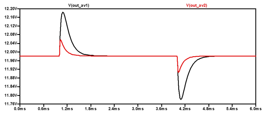
Figure 31: Transient response comparison of solution 1 (black) and 2 (red) (LTspice simulation)
09. IMPACT OF OPTOCOUPLER CTR VARIATIONS
Previous expression E.35 shows that the midband gain of the compensator is directly proportional to the optocoupler CTR, as follows:
 (44)
(44)
Theoretically, CTR variations will shift the magnitude curve of the compensator up or down, leaving the phase curve unchanged. In reality, CTR and pole frequency are linked and as the CTR increases, the pole frequency reduces causing a lower phase boost of the compensator. The result is a different crossover frequency of the open-loop transfer function and a different phase margin. For this reason, the system response must be assessed at the CTR limits.
For the case of this design, the CTR range at full-load and minimum input voltage condition is:
 (45)
(45)
Fixing the pole frequency for the sake of the example, it can be observed how for the CTR range considered, the midband gain varies as -2.8 dB (CTR = 0.4), 1.47 dB (CTR = 0.65) and 4.2 dB (CTR = 0.9).
The effect of this in the open-loop crossover frequency and phase margin is shown in Figure 32. The crossover frequency is found in the range between 1.75 kHz and 3.7 kHz (target was 3 kHz), and the phase margin in the range 75.2° and 66.5°. In this case, the soft slope of the phase curve ensures that small variations in component parameters do not have a strong impact in the phase margin. Note that in practice, the impact of the pole frequency variations along with CTR can cause a higher phase margin deviation, and this is not shown in Figure 33.
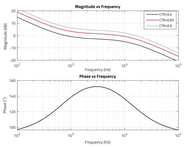
Figure 32: Compensator response versus CTR (MATLAB)
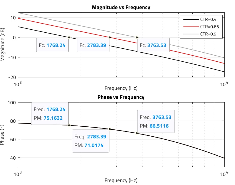
Figure 33: Figure 33. Open-loop transfer function: Fc and PM versus CTR (MATLAB)
010. DESIGN PROTOTYPE AND EXPERIMENTAL RESULTS
A 30 W Flyback converter prototype based on the specification of section 3 has been built (Figure 34). An optocoupler WL-OCPT from the 817 series and Bin A with a static CTR of 0.71 at the DC-Bias conditions shown in previous section 5.2 was used for the measurements. Note that experimental results in this section are for Vin_min = 36 V and full load Iout = 2.5 A as designed, but feedback loop stability (phase and gain margins) must still be checked for all other expected operating conditions of the power supply and any required adjustments performed.
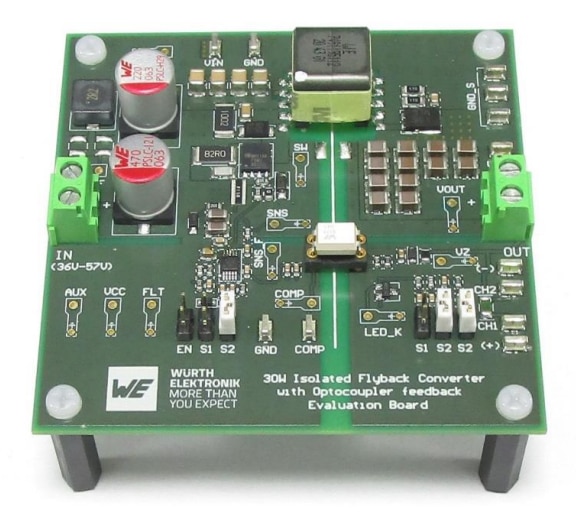
Figure 34: Current-mode Flyback converter with optocoupler board
10.1 Measured Plant Frequency Response
The control-to-output transfer function shows a magnitude and phase in good agreement with analytical results, as shown in Figure 35.
For 3 kHz, analytical results showed gain and phase of -2.1 dB and -82.4°, respectively (Figure 25), close to the measured values of -2.1 dB and -79.4°. For 10 kHz, analytical results were -12.3 dB and -96.3° (Figure 12), also a good approximation to the measured -12.1 dB and -99°.
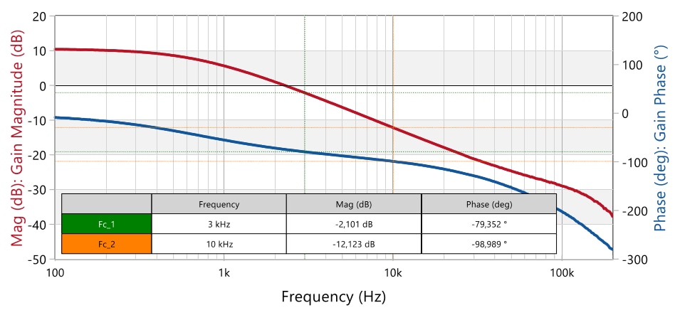
Figure 35: Measured Plant (control-to-output) magnitude and phase frequency response (Vin = 36 V, Iout = 2.5 A) (Bode100)
10.2 Results for Compensator Design 1
The compensator in design solution 1 was designed for 2.3 dB gain and 154° phase at 3 kHz (Figure 26). Experimental results show a gain of 2.66 dB and a phase of 155.9° (Figure 36). This is close but not exact since there are different factors affecting the measured values in a real prototype. As previously mentioned, the optocoupler small-signal CTR is slightly higher than the static CTR of 0.71 considered in the design, increasing the measured midband gain. This is partially offset by the reduction in midband gain caused by Rb diverting some current from the optocoupler LED, and the non-ideal AC decoupling provided by the Zener network. The non-exact cancellation of the zero and optocoupler pole can also contribute to differing results. The open-loop response shows a crossover frequency of 3.2 kHz with a phase margin of 75.5° and a gain margin of 19.6 dB (Figure 37). The phase margin is higher than the 70° targeted due to the addition of the compensator and plant excess phase. Although this is a robust and very stable design, the compensator can be further ‘fine-tuned’ for example, by reducing C1 in order to set a higher zero frequency to reduce the compensator phase boost and with it, reduce the phase margin to the target 70°.
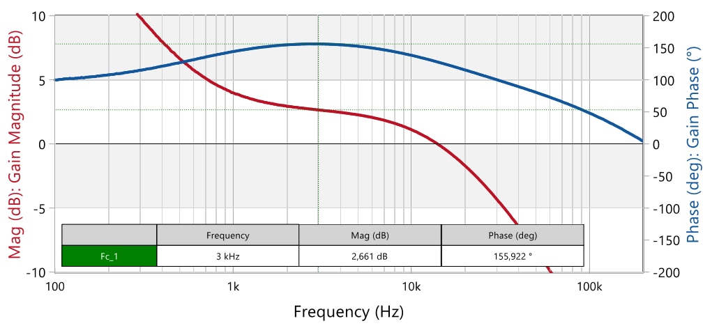
Figure 36: Measured compensator magnitude and phase frequency response for compensator design 1 (Vin = 36 V, Iout = 2.5 A) (Bode100)
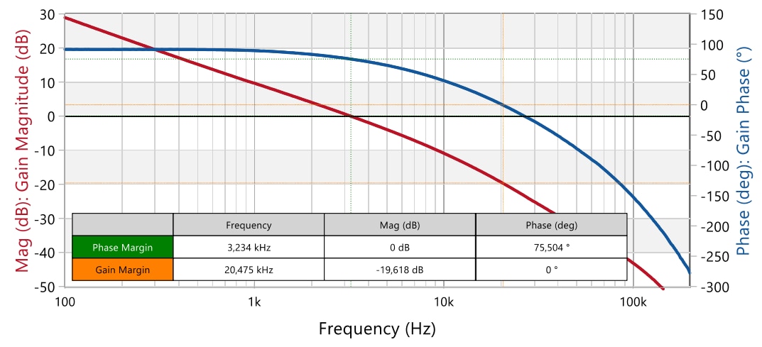
Figure 37: Measured open-loop magnitude and phase frequency response for compensator design 1 (Vin = 36 V, Iout = 2.5 A) (Bode100)
10.3 Results for Compensator Design 2
The compensator shows a gain of around 12.5 dB and a phase of 159.3° at 10 kHz, and it is observed how it presents a Type 2 characteristic due to the cancellation of the optocoupler pole with the added zero (Figure 38). Analytical results were 11.6 dB and 165° (Figure 28). The cause for the higher gain has been explained in the previous section. A lower phase boost can be caused by a non-ideal cancellation of the zero and the optocoupler pole. However, in this case the main cause seems to be the two additional high-frequency poles appearing at around 100 kHz in the response, as it is observed how the gain rolls off at around -60 dB/dec after the compensator pole and the phase is on its way to -90° (instead of 90°). These poles were not modelled and contribute a small phase lag at 10 kHz. A possible adjustment to increase the compensator phase boost can be to shift the compensator pole at a higher frequency and/or the zero cancelling the optocoupler pole at a lower frequency. The excess gain provided by the compensator causes an open-loop crossover frequency of 10.2 kHz, higher than the designed result of 9.2 kHz. The phase margin is below the 70° target at around 59° with a gain margin of around 10 dB (figure 39). Although the design is stable, the phase margin can be further increased as explained above. Note that reducing the crossover frequency with a lower compensator midband gain (lower R2) can help not only to increase the phase margin but also the gain margin in this case.
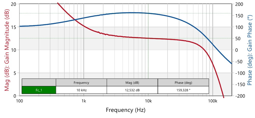
Figure 38: Measured compensator magnitude and phase frequency response for compensator design 2 (Vin = 36 V, Iout = 2.5 A) (Bode100)
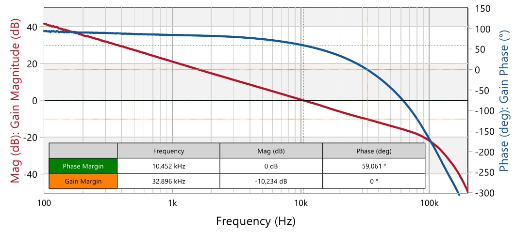
Figure 39: Measured open-loop magnitude and phase frequency response for compensator design 2 (Vin = 36 V, Iout = 2.5 A) (Bode100)
10.4 Load Transient Response Measurement
Results of the load transient response for both compensator design solutions are shown in Figure 40 (design 1 with fc = 3.2 kHz and PM = 75.5°) and in Figure 41 (design 2 with fc = 10.4 kHz and PM = 59°). Note that the axis scale on both oscilloscope captures is the same for direct comparison. Although with a difference in the phase margin, the results are still in line with those from LTspice simulation shown in previous Figure 31. As expected, a faster response with lower over- and undershoot as well as a faster settling time is obtained with a higher crossover frequency and a lower phase margin of the open-loop response (design 2).
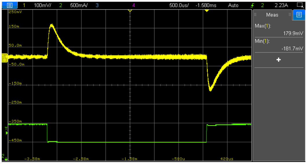
Figure 40: Load transient response for compensator design 1 (Vin = 36 V, fc = 3.2 kHz, PM = 75.5°)) (Iout = 2 A to 2.5 A current step at 1 A/µs)
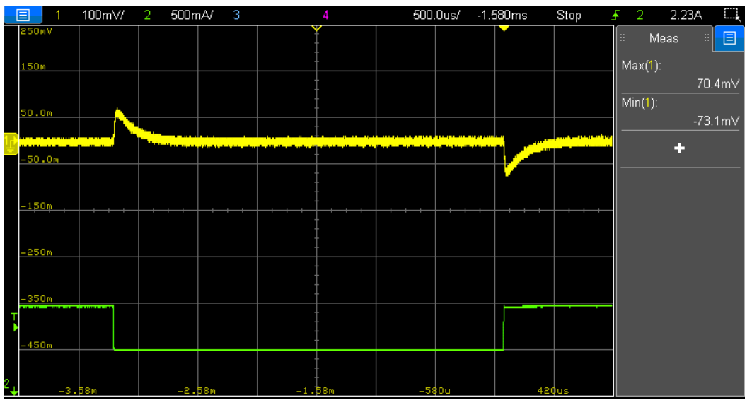
Figure 41: . Load transient response for compensator design 2 (Vin = 36 V, fc = 10.4 kHz, PM = 59°) (Iout = 2 A to 2.5 A current step at 1 A/µs)
10.5 Results for CTR variation
Experimental results shown previously were obtained with a WL-OCPT 817 device from bin A and a CTR of 0.7 at the DC-Bias conditions of Vce= 2.7 V and Ic = 0.46 mA. It was seen in previous section 5.2 that the expected maximum CTR for such binning and DC-Bias is 0.9. In order to assess the impact of CTR variation, the converter stability for both compensator designs has been additionally tested with an optocoupler from bin B measuring a CTR of 0.9 at the stated DC-Bias conditions. It is observed in both cases how the higher CTR causes a higher open-loop crossover frequency as expected, since it increases the compensator midband gain. The phase curve rolls off with increasing frequency causing a reduction of the phase margin. In addition to this, the optocoupler pole frequency decreases with increasing CTR, lowering the compensator phase boost. These are the reasons why the highest CTR represents the worst-case in this particular design.
Although experimental results show a stable control loop, if the compensator had been designed considering the maximum CTR of 0.9 instead of 0.71 as in this document (middle of CTR range), a higher phase margin would be ensured for all other optocoupler devices within the selected binning.
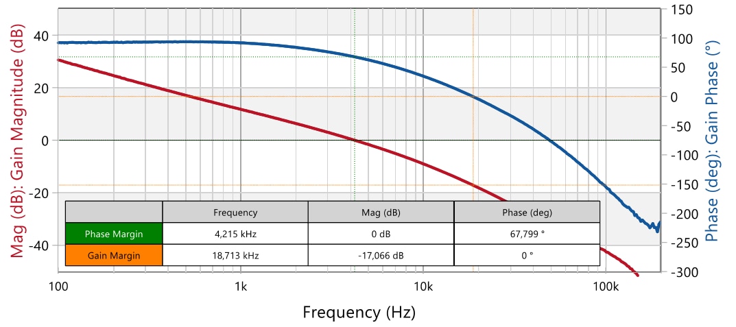
Figure 42: Measured open-loop response for compensator design 1 (WL-OCPT with CTR=0.9) (Vin = 36 V, Iout = 2.5 A) (Bode100)

Figure 43: Measured open-loop response for compensator design 2 (WL-OCPT with CTR=0.9) (Vin = 36 V, Iout = 2.5 A) (Bode100)
10.6 Test setup
Figure 44 shows the test setup used for frequency response measurement (open-loop response). A Bode100 device with a B-WIT
injection transformer both from Omicron Lab were used. A resistor load (4.7 Ω) draws 2.55 A output current (full load). Note that electronic loads should be better avoided for this test.
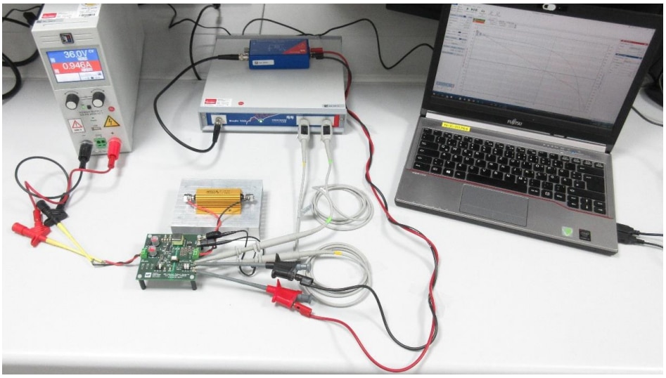
Figure 44: Test setup for transfer function / frequency response measurement
The test setup in Figure 45 was used to measure the load transients with a load current step of 2 A to 2.5 A. A 6-Ω resistor (2 x 3 Ω in series used in the setup) draws a constant output current of 2 A. A 25-Ω resistor is connected in parallel with the 6 Ω via a switched MOSFET with dynamic gate control. It draws the additional 0.5 A required for the load current step with the desired rise and fall dI/dt.
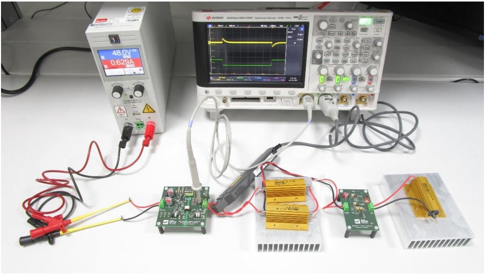
Figure 45: Test setup for load transient response measurement
011. SUMMARY AND CONCLUSION
Optocouplers are widely used to transmit the feedback signal across the isolation barrier in isolated power supplies. The optocoupler is therefore part of the compensator block and its parameters affect the compensator transfer function. A very popular compensator configuration uses a TL431 with an optocoupler, whose minimum current-transfer-ratio (CTR) value needs to be found for DC-bias design, and its full CTR range in order to analyze system performance. Variations in the CTR will shift the magnitude curve of the compensator transfer function up or down, leading to a different crossover frequency and in turn, a different phase margin of the open-loop transfer function. Another important consideration is the parasitic collectoremitter capacitance of the optocoupler phototransistor, which limits the optocoupler bandwidth. This parasitic capacitance is typically used to set the compensator pole for systems with low crossover frequency like offline AC-DC converters. For higher crossover frequencies, like in the example shown in this document, the limitation of the optocoupler pole can be eliminated by introducing an additional zero and pole in the compensator. In any case, the optocoupler CTR and pole frequency play a key role in the control loop and their value and tolerance variations need to be considered in the design. Example procedures to find the CTR range as well as the optocoupler pole frequency have been provided, and their impact in the control loop has been shown. In addition to highlighting the optocoupler role in the system, the compensator design covered in this document illustrated a step-by-step example procedure to stabilize a current-mode Flyback converter operating in CCM.
A Appendix
A.1 Measuring WL-OCPT Optocoupler CTR
The current transfer ratio of the optocoupler can be measured in different ways and with different measurement equipment. In the example setup of figure 46, the voltage Vdd and the collector or emitter resistance value ‘R’ are both set as in the design (in this case: R = Rc = 5 kΩ, Vdd = 5 V). The same resistance value is selected on the LED side, and a signal generator is used to output a low-amplitude sinusoidal waveform with a DC offset adjusted to provide the required LED bias current to set Vce to the target value (in this case Vce = 2.7 V for full load, which gives V2 = 2.3 V). With an oscilloscope, the voltages V1 and V2 are probed, and the CTR directly found by the ratio of the average values for DC, and the peak-to-peak values for AC, as below:
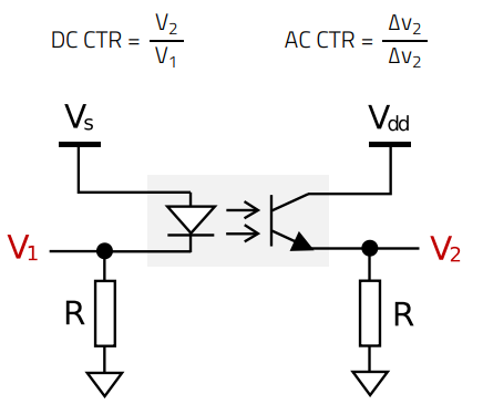 (46)
(46)
Figure 46: Example setup for measuring static and dynamic CTR values of WL-OCPT optocoupler
A.2 Measuring WL-OCPT Optocoupler Pole Frequency
The optocoupler pole frequency can also be measured with different techniques. Figure 47 shows an example measurement setup using a vector network analyzer (VNA) (e.g. Bode100) with an injection transformer (e.g. B-WIT 100
). The setup considerations are like for the CTR measurement above, with the DC source Vin adjusted to provide the LED bias current required to set the target Vce voltage. Note that voltages V1 and V2 should be checked with an oscilloscope at low frequency (at least a decade lower than the pole frequency) to ensure the sinusoidal waveforms are not clipped or distorted. If so, the amplitude of the injected AC voltage or the resistance Rs (normally between 10 and 100 Ω) will need to be reduced. A typical measurement result is shown in previous Figure 24.
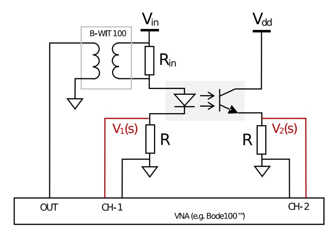
Figure 47: Example setup for measuring pole frequency of WL-OCPT optocoupler with a Vector Network Analyzer (VNA)
A.3 References
[1] C. Basso, Transfer Functions of Switching Converters, Faraday Press, 2021
[2] C. Basso, Switch-Mode Power Supplies: SPICE Simulations and Practical Designs, Second Edition McGraw-Hill Professional, 2014
[3] C. Basso, Designing Control Loops for Linear and Switching Power Supplies: A Tutorial Guide, Artech House, 2012
[4] D.Venable, “The K factor: a new mathematical tool for stability analysis and synthesis”, Proceedings from Powercon10, 1983, San Diego
[5] R.W.Eriksson, D.Maksimović, Fundamentals of Power Electronics, Second Edition, Springer, 2001
[6] V. Vorpérian, “Simplified Analysis of PWM Converters Using Model of PWM Switch Part 1: Continuous Conduction Mode”, Transactions on Aerospace and Electronics Systems, 1990.
[7] V. Vorpérian, “Simplified Analysis of PWM Converters Using Model of PWM Switch Part 2: Discontinuous Conduction Mode”, Transactions on Aerospace and Electronics Systems, 1990.
[8] WE-PoEH 7491195112 Datasheet, Würth Elektronik
[9] NCP12700 Datasheet, Onsemi
[10] TL431 Datasheet, Nexperia
[11] WL-OCPT 817 phototransistor optocoupler series Datasheet, Würth Elektronik
[12] ANO007: Understanding Phototransistor Optocouplers, Application note, Würth Elektronik
[13] ANO006: Lifetime of Optocoupler, Application note, Würth Elektronik

