


Support Note
Isolated RS-485 interface based on 4-channel digital isolator with integrated DC/DC converter
SN026 by Artem Beliakov
This design example shows an isolated RS-485 interface using a 4-channel reinforced digital isolator with an integrated DC/DC converter, reducing component count and board space. The design is optimized for half-duplex operation at data rates up to 10 Mbps and meets CISPR 32 Class B radiated emission standard.
1. OVERVIEW OF RS-485
The RS-485 interface is widely used in industrial and commercial applications due to its robustness, long-distance data transmission capabilities, and resilience to electrical noise. RS-485 supports multiple devices on a single bus, making it ideal for complex systems and distributed networks. The main features of this interface include:
- Long-Distance Communication: Can transmit data up to 1200 meters at lower data rates (up to 100 kbps)
- Flexible Data Rates: Supports data rates from a few kbps up to 10 Mbps for short distances (~15 meters), with the data rate decreasing as the distance increases. However, with today's technology, signal rates beyond the specification of up to 50 Mbps are possible.
- Multi-Device Support: Allows up to 32 devices on a single bus (32-unit load (UL) or up to 256 low-unit-load transceivers where one transceiver is 1/8 UL), providing flexible connectivity for multi-node systems.
- Differential Signaling: Using differential signaling (balanced line), achieves high immunity to electrical noise, making it suitable for environments with significant EMI.
Thanks to these benefits, RS-485 is widely used in industrial automation, building automation, energy management, motor control and renewable energy systems, where stable and noise-resistant data communication is essential for reliable operation in demanding environments.
2. IMPORTANCE OF RS-485 ISOLATION
The differential nature of RS-485 signaling helps reduce noise, but it can still be affected by strong electromagnetic interference (EMI). For this reason, isolation is very important in modern applications where harsh conditions and high electrical noise levels are common. Isolated RS-485 provides extra protection and improves performance by separating the communication lines from the system ground, offering several benefits:
- Protection Against Ground Loops: Isolation prevents issues caused by ground potential differences, ensuring stable communication in large-scale systems with distributed equipment.
- Noise Immunity: Isolation (along with additional measures such as filtering, shielding and proper PCB layout) protects sensitive equipment from high levels of EMI and strong magnetic fields often found in industrial environments, helping maintain data integrity.
- Surge and Transient Protection: Galvanic isolation, complemented by surge protection devices (such as TVS diodes), allows to withstand voltage surges and transients, protecting components and improving the system's overall reliability.
- Safety in High-Voltage Applications: In systems such as energy meters and renewable energy, isolation helps protect low-voltage control systems from high-voltage sections, ensuring operator and equipment safety.
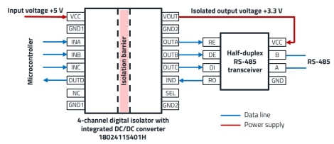
Figure 1: Block diagram of isolated half-duplex RS-485 interface.
3. DESCRIPTION OF DESIGN EXAMPLE BOARD
3.1 Key parameters
The board is optimized for a data rate of 10 Mbps and a shielded twisted cable length of 10 m (distance between the transmitter and receiver boards during radiated emission test).
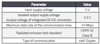
Table 1: Key parameters of isolated RS-485 board.
The integrated DC/DC converter within the digital isolator cannot operate in boost mode therefore the output voltage must be less than or equal to the input voltage (VCC). In the design example the output voltage selection pin (SEL) of the digital isolator is connected to the ground (GND2) for 3.3 V output voltage.
3.2 Configuration
The top view of the application example board is shown in Figure 2. The board can be conditionally divided into 8 blocks:
- Pins A and B: non-inverting and inverting bidirectional bus data lines (RS-485 input)
- Filter circuit of the data lines and TVS diodes for overvoltage protection
- Half-duplex RS-485 transceiver in SOIC-8NB package
- 4-channel digital isolator with integrated isolated DC/DC converter
- Filter circuit of the DC supply voltage line
- Terminal block screw connector for power supply
- THT 3-pin header for signals from controller
- SMA connectors for RS-485 interface signals*
* The SMA connectors (high-speed connectors) are used for a test signal feed by a signal generator into the PCB. This is a simulation of a single ended board level signal source feeding the signal to the digital isolator.
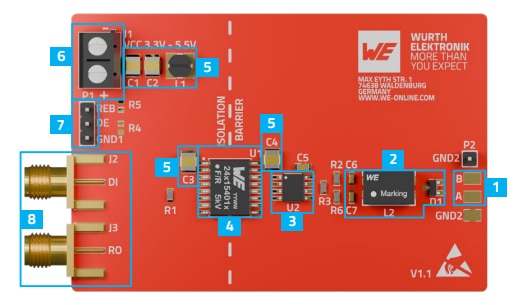
Figure 2: Top view of the application example board.
Figure 3 shows the schematic of the transceiver and receiver boards used during the radiated emission test. The differences between the boards are detailed in Section 6.1.
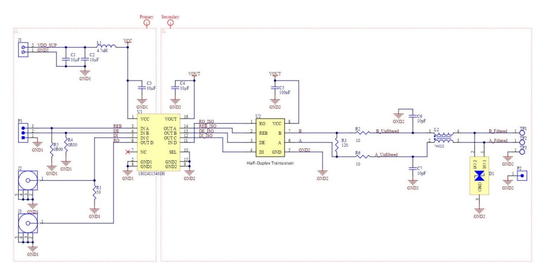
Figure 3: Schematic of isolated half-duplex RS-485 transceiver and receiver boards.
4. SELECTION OF COMPONENTS
4.1 Digital Isolator 18024115401H
The 18024115401H is a 4-channel digital isolator with an integrated isolated DC/DC converter that provides up to 0.65 W of isolated power (for power supply of internal structure of the digital isolator and the half-duplex RS-485 transceiver) in a SOIC-16WB package. The availability of an integrated DC/DC converter significantly reduces the number of components in the design saving board space. In addition, the converter has integrated protection systems that guard against thermal overstress with thermal shutdown and protect against electrical damage using overcurrent, shortcircuit and undervoltage circuitry. The 18024115401H has a 3/1 channel configuration (3 forward and 1 reverse channels). This channel configuration is required for normal operation of the isolated RS-485 interface in half-duplex transmission. Two forward channels of the 18024115401H are used to isolate control signals from a microcontroller that switch the half-duplex RS-485 transceiver (RE and DE pins) between transmit and receive modes. The other two channels of the digital isolator (1 forward and 1 reverse) are used to isolate bus interface signals passing through the half-duplex RS-485 transceiver (DI and RO pins) in transmit and receive modes.
Key Features of the 18024115401H:
- 4-channel digital isolator with integrated 0.65 W Isolated DC/DC converter;
- UL1577 recognized:
- 5000 VRMS isolation voltage for 60 s;
- DIN EN IEC 60747-17 (VDE 0884-17):2021-10 certified:
- Reinforced isolation;
- Maximum repetitive peak isolation voltage: 1414 VPK;
- Maximum working isolation voltage: 1000 VRMS and 1414 VDC;
- Maximum transient isolation voltage: 7070 VPK ;
- Maximum surge isolation voltage: 7070 VPK ;
- Input voltage range: 3.15 V to 5.5 V;
- User-selectable output voltage: 3.3 V or 5 V;
- Data rate up to 100 Mbps;
- ±150 kV/µs typ. CMTI;
- Complies with EN55032 (CISPR-32) class B conducted and radiated emissions standard (with the reference layout specified in the data sheet);
- Ambient temperature range: -40°C to 125°C.
4.2 Half-Duplex RS-485 Transceiver
Half-duplex RS-485 transceivers provide bidirectional communication over a single pair of wires by alternating between transmitting and receiving data. This allows multiple devices to share the same communication line efficiently, reducing the number of required wires and simplifying system design. The design example uses a standard half-duplex RS485 transceiver in the SOIC-8NB package.
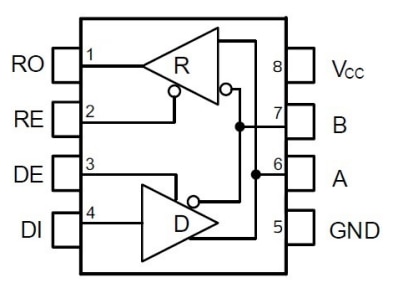
Figure 4: Simplified block diagram of non-isolated half-duplex RS-485 transceiver in SOIC-8NB package.
4.3 Transient Protection
The WE-TVS diode 824022 (two bidirectional TVS diodes in SOT-23 package) with a channel operating voltage of 5 V were selected to protect data line from overvoltage. The 824022 TVS diode has a very low input capacitance (15 pF), which helps minimize signal distortion, maintain high data rates and preserve the integrity of differential signals in highspeed RS-485 communication systems.
4.4 Filter circuit of the RS-485 data lines
The WE-SL2 744222 common mode line filter was selected to the filter the RS-485 data lines. A detailed description of how to select the right components for the filter can be found in the Application Note ANP083 ‘’Adapter PCB for filtering electromagnetic interference on an RS-485 interface’’ (Section 2.1 Filter circuit of the data lines).
4.5 Filter circuit of the supply voltage line
The WE-PD2 SMT power inductor 744773047 (4.7 µH) and WCAP-CSGP MLCC chip ceramic capacitors 885012209014 (10 µF/16 V, X7R, 1210) were selected for the input and output filter of the integrated DC/DC converter. For detailed information on filter selection and layout of the converter, refer to the 18024x15401x digital isolator datasheet (Section 20 Design example) and the online tool, REDEXPERT EMI Filter Designer.
5. REDUCING COMMON-MODE INTERFERENCE WITH OVERLAPPING STITCHING CAPACITANCE
The 18024115401H digital isolator provides galvanic isolation between the input and output of the system, but parasitic coupling capacitance of an isolation barrier allows common mode currents to flow. As a result, the isolator may be a source of common-mode interference. Typically, design engineers address this issue using an external Y-capacitor between the input and output. However, an alternative approach is to utilize the parasitic capacitance between PCB layers as an integrated Y-capacitor. This method, commonly referred to as stitching capacitance, provides an effective high-frequency return path for common-mode noise, reducing EMI without requiring external components.
Careful attention needs to be taken regarding the layout to meet any safety isolation standards. Depending on the targeted safety standard the requirements applying to inner layers for thickness and distance along a cemented joint. The outer layers and any exposed inner layer edges are subject to the creepage and clearance rules. This design example is designed to meet reinforced isolation.
This design example board has a 4-layer PCB structure. The stitching capacitance is formed by the parasitic properties of overlapping copper planes in different PCB layers (between internal layer 1, internal layer 2 and bottom layer). The PCB layers and the overlap that form the stitching capacitance of the board are shown in Figure 5.
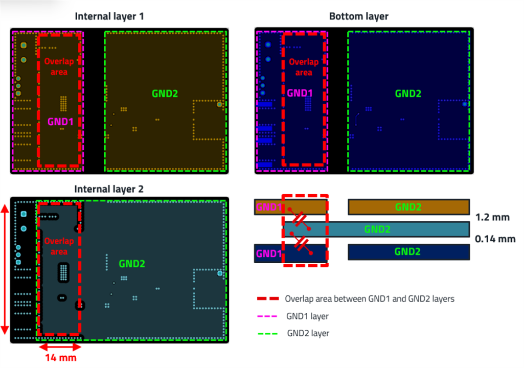
Figure 5: Overlap area of isolated RS-485 design example board
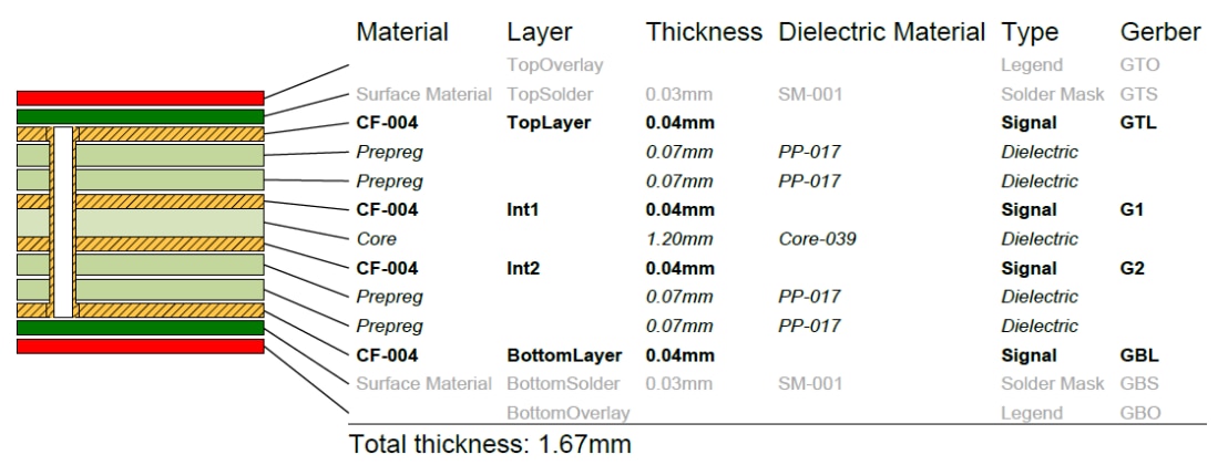
Figure 6: Layer stack legend.
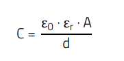
The parasitic capacitance between two overlapping PCB planes can be approximated by the parallel plate capacitance formula:
 (1)
(1)
Where:
- C is the stitching capacitance in farads (F);
- ε0 is the vacuum permittivity ≈ 8.854×10⁻¹² F/m;
- εr is the relative dielectric constant of the PCB material (this information is provided by a PCB manufacturer, typically 4-5);
- A is the overlapping area of the planes in square meters (m²);
- d is the distance between the planes (dielectric thickness) in meters (m).
Key parameters of the board for the stitching capacitance calculation:
- Overlap area (between GND1 and GND2 layers): 14 x 44 mm2 = 616 mm2;
- Distance between overlap layers and relative dielectric constant:
- Internal layer 1 to internal layer 2: 1.2 mm, εr= 4.6;
- Internal layer 2 to bottom layer: 0.14 mm, εr= 4.
The total stitching capacitance of the PCB is the sum of the capacitances between the two overlapping regions:
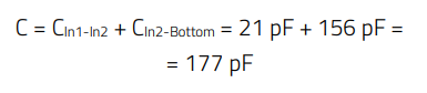 (2)
(2)
The approximate stitching capacitance of the design is 177 pF, providing an effective high-frequency return path for common-mode noise and significantly improving EMI performance. Measurements of radiated emissions demonstrate the success of this approach (Figure 9), as the 4-layer board with stitching capacitance remains well below the required limits, proving that this integrated design effectively suppresses common-mode interference. More detailed information about common mode interference and coupling capacitance can be found in Application Note ANS022.
6. TESTING
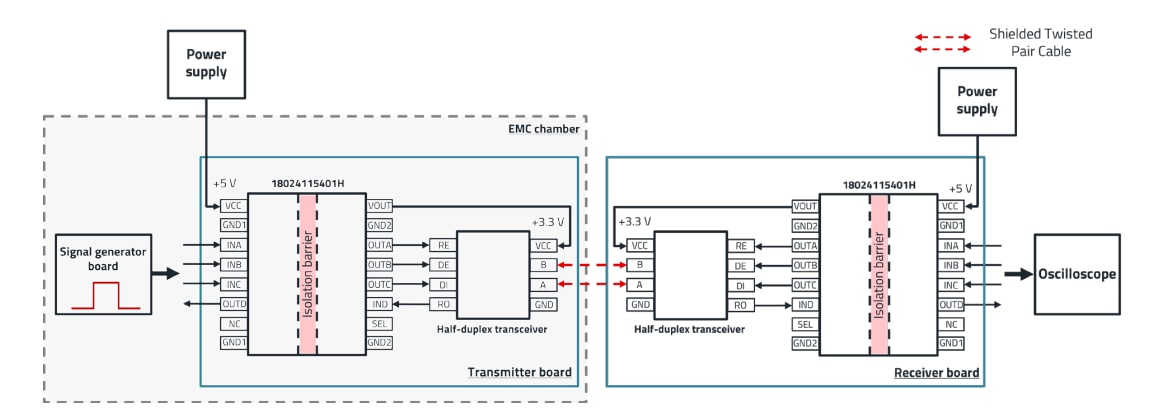
6.1 Test Setup
The test setup for the radiated emission measurement is shown in Figure 7.
The configuration differences between the transmitter and the receiver boards are:
- The transmitter board: resistors R4 and R5 are not installed.
- The receiver board: resistors R4 and R5 are installed.
6.2 Radiated Emission
Measurements made with 10 m shielded twisted cable length between transmitter and receiver boards and 10 Mbps data rate.
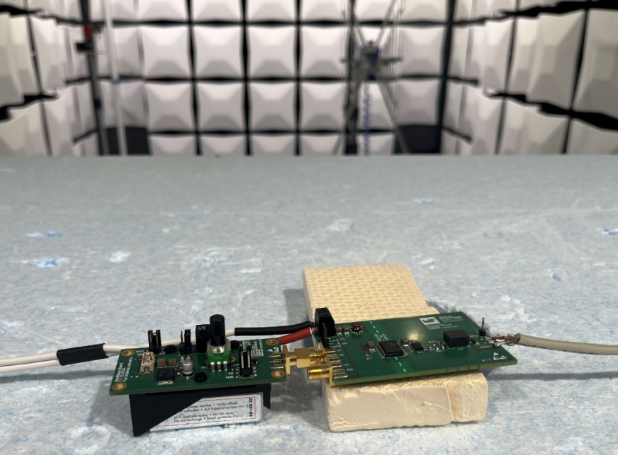
Figure 8: Transmitter board and signal generator board in EMC test chamber.
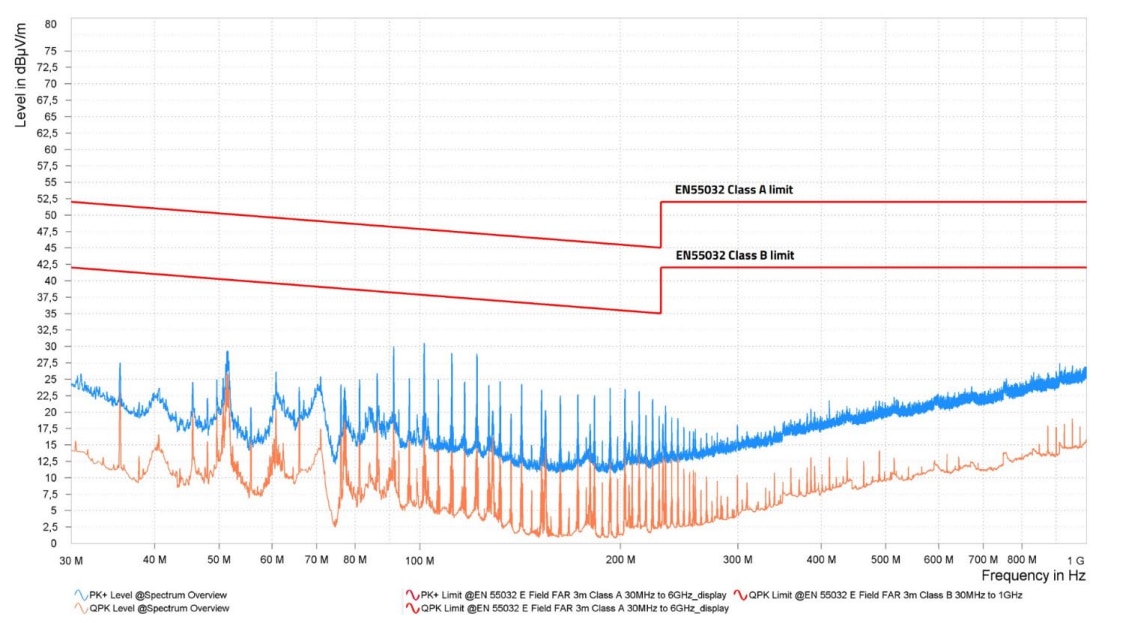
Figure 9: Radiated emission (CISPR 32 Class B).
6.3 Propagation Delay
The propagation delay between the input and output signals of the digital isolator is ~15 ns (Figure 10), ensuring fast switching, minimal signal distortion and stable communication via the RS-485 interface.
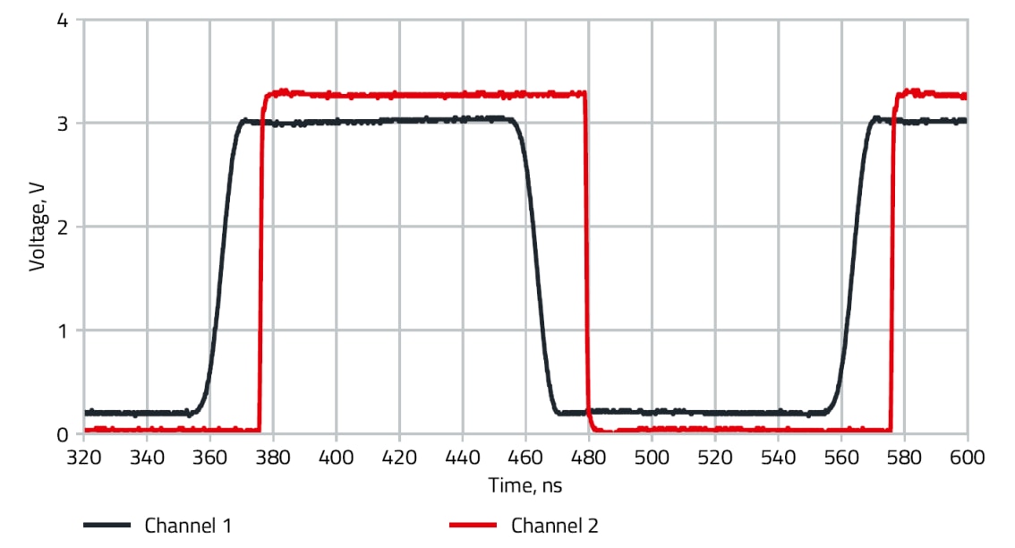
Figure 10: Propagation delay between input (Channel 1) and output (Channel 2) signals of the digital isolator 18024115401H.
A APPENDIX
A.1 Bill of Material
| Designator | Description | WE series | Order Code | Manufacturer | Quantity |
| C1, C2 | Filter ceramic chip capacitor 10 µF, 16 V, X7R, 1210 | WCAP-CSGP | 885012209014 | Würth Elektronik | 2 |
| C3, C4 | Ceramic chip capacitor 10 µF, 16 V, X7R, 1210 | WCAP-CSGP | 885012209014 | Würth Elektronik | 2 |
| C5 | Ceramic chip capacitor 100 nF, 100 V, X7R, 0805 | WCAP-CSGP | 885012207128 | Würth Elektronik | 1 |
| C6, C7 | Ceramic chip capacitor 10 pF, 25 V, NP0, 0603 | WCAP-CSGP | 885012006032 | Würth Elektronik | 2 |
| R1 | SMD resistor 50 Ω, 0.1 W, 0603 | 1 | |||
| R2, R6 | SMD resistor 10 Ω , 0.1 W, 0603 | WRIS-RSKS | 560112116013 | Würth Elektronik | 2 |
| R3 | SMD resistor 120 Ω , 0.1 W, 0603 | WRIS-RSKS | 560112116119 | Würth Elektronik | 1 |
| R4,R5 | SMD resistor 0 Ω , 0.1 W, 0603 | WRIS-RSKS | 560112116001 | Würth Elektronik | 2 |
| U1 | 4-channel digital isolator with integrated DC/DC, SOIC-16WB | WPME-CDIP | 18024115401H | Würth Elektronik | 1 |
| U2 | Half-duplex RS-485 transceiver 50 Mbps, SOIC-8NB | 1 | |||
| D1 | 2-channel TVS Diode, 5 V, 12 pF, SOT23-3L | WE-TVS | 824022 | Würth Elektronik | 1 |
| L1 | Filter SMD inductor 4.7 µH, 4532 | WE-PD2 | 744773047 | Würth Elektronik | 1 |
| L2 | SMT common mode line filter 1000 µH, 0.8 A, 80 V | WE-SL2 | 744222 | Würth Elektronik | 1 |
| J1 | THT horizontal entry modular, pitch 5 mm, 2p | WR-TBL | 691502710002 | Würth Elektronik | 1 |
| J2, J3 | SMA PCB end launch connector | WR-SMA | 60312202114509 | Würth Elektronik | 2 |
| P1 | THT 3-pin header, vertical, single row, pitch 2.54 mm | WR-PHD | 61300311121 | Würth Elektronik | 1 |
| P2 | THT 1-pin header, vertical, single row, pitch 2.54 mm | WR-PHD | 61300111121 | Würth Elektronik | 1 |
A.2 Supporting design file archive
Supporting design file archive contains Support Note, Schematic, Bill of materials, Gerber files, NC Drill files, Support Note, Layer Definition and Layer Stack Legend. The link to the file archive is available:
https://www.we-online.com/components/products/media/860161
IMPORTANT NOTICE
The Application Note is based on our knowledge and experience of typical requirements concerning these areas. It serves as general guidance and should not be construed as a commitment for the suitability for customer applications by Würth Elektronik eiSos GmbH & Co. KG. The information in the Application Note is subject to change without notice. This document and parts thereof must not be reproduced or copied without written permission, and contents thereof must not be imparted to a third party nor be used for any unauthorized purpose. Würth Elektronik eiSos GmbH & Co. KG and its subsidiaries and affiliates (WE) are not liable for application assistance of any kind. Customers may use WE’s assistance and product recommendations for their applications and design. The responsibility for the applicability and use of WE Products in a particular customer design is always solely within the authority of the customer. Due to this fact it is up to the customer to evaluate and investigate, where appropriate, and decide whether the device with the specific product characteristics described in the product specification is valid and suitable for the respective customer application or not. The technical specifications are stated in the current data sheet of the products. Therefore the customers shall use the data sheets and are cautioned to verify that data sheets are current. The current data sheets can be downloaded at www.we-online.com. Customers shall strictly observe any product-specific notes, cautions and warnings. WE reserves the right to make corrections, modifications, enhancements, improvements, and other changes to its products and services. WE DOES NOT WARRANT OR REPRESENT THAT ANY LICENSE, EITHER EXPRESS OR IMPLIED, IS GRANTED UNDER ANY PATENT RIGHT, COPYRIGHT, MASK WORK RIGHT, OR OTHER INTELLECTUAL PROPERTY RIGHT RELATING TO ANY COMBINATION, MACHINE, OR PROCESS IN WHICH WE PRODUCTS OR SERVICES ARE USED. INFORMATION PUBLISHED BY WE REGARDING THIRD-PARTY PRODUCTS OR SERVICES DOES NOT CONSTITUTE A LICENSE FROM WE TO USE SUCH PRODUCTS OR SERVICES OR A WARRANTY OR ENDORSEMENT THEREOF. WE products are not authorized for use in safety-critical applications, or where a failure of the product is reasonably expected to cause severe personal injury or death. Moreover, WE products are neither designed nor intended for use in areas such as military, aerospace, aviation, nuclear control, submarine, transportation (automotive control, train control, ship control), transportation signal, disaster prevention, medical, public information network etc. Customers shall inform WE about the intent of such usage before design-in stage. In certain customer applications requiring a very high level of safety and in which the malfunction or failure of an electronic component could endanger human life or health, customers must ensure that they have all necessary expertise in the safety and regulatory ramifications of their applications. Customers acknowledge and agree that they are solely responsible for all legal, regulatory and safety-related requirements concerning their products and any use of WE products in such safety-critical applications, notwithstanding any applicationsrelated information or support that may be provided by WE. CUSTOMERS SHALL INDEMNIFY WE AGAINST ANY DAMAGES ARISING OUT OF THE USE OF WE PRODUCTS IN SUCH SAFETYCRITICAL APPLICATION.
DIRECT LINK
USEFUL LINKS:
Application Notes : https://we-online.com/en/support/knowledge/application-notes
Services: https://we-online.com/en/products/components/service
Contact : https://we-online.com/en/support/contact
CONTACT INFORMATION
Würth Elektronik eiSos GmbH & Co. KG
Max-Eyth-Str. 1, 74638 Waldenburg, Germany
Tel.: +49 (0) 7942 / 945 – 0
Email: appnotes@we-online.de