element14 Community
element14 Community
    Register Log In
  • Site
  • Search
  • Log In Register
  • Community Hub
    Community Hub
    • What's New on element14
    • Feedback and Support
    • Benefits of Membership
    • Personal Blogs
    • Members Area
    • Achievement Levels
  • Learn
    Learn
    • Ask an Expert
    • eBooks
    • element14 presents
    • Learning Center
    • Tech Spotlight
    • STEM Academy
    • Webinars, Training and Events
    • Learning Groups
  • Technologies
    Technologies
    • 3D Printing
    • FPGA
    • Industrial Automation
    • Internet of Things
    • Power & Energy
    • Sensors
    • Technology Groups
  • Challenges & Projects
    Challenges & Projects
    • Design Challenges
    • element14 presents Projects
    • Project14
    • Arduino Projects
    • Raspberry Pi Projects
    • Project Groups
  • Products
    Products
    • Arduino
    • Avnet & Tria Boards Community
    • Dev Tools
    • Manufacturers
    • Multicomp Pro
    • Product Groups
    • Raspberry Pi
    • RoadTests & Reviews
  • About Us
  • Store
    Store
    • Visit Your Store
    • Choose another store...
      • Europe
      •  Austria (German)
      •  Belgium (Dutch, French)
      •  Bulgaria (Bulgarian)
      •  Czech Republic (Czech)
      •  Denmark (Danish)
      •  Estonia (Estonian)
      •  Finland (Finnish)
      •  France (French)
      •  Germany (German)
      •  Hungary (Hungarian)
      •  Ireland
      •  Israel
      •  Italy (Italian)
      •  Latvia (Latvian)
      •  
      •  Lithuania (Lithuanian)
      •  Netherlands (Dutch)
      •  Norway (Norwegian)
      •  Poland (Polish)
      •  Portugal (Portuguese)
      •  Romania (Romanian)
      •  Russia (Russian)
      •  Slovakia (Slovak)
      •  Slovenia (Slovenian)
      •  Spain (Spanish)
      •  Sweden (Swedish)
      •  Switzerland(German, French)
      •  Turkey (Turkish)
      •  United Kingdom
      • Asia Pacific
      •  Australia
      •  China
      •  Hong Kong
      •  India
      •  Korea (Korean)
      •  Malaysia
      •  New Zealand
      •  Philippines
      •  Singapore
      •  Taiwan
      •  Thailand (Thai)
      • Americas
      •  Brazil (Portuguese)
      •  Canada
      •  Mexico (Spanish)
      •  United States
      Can't find the country/region you're looking for? Visit our export site or find a local distributor.
  • Translate
  • Profile
  • Settings
Experts, Learning and Guidance
  • Technologies
  • More
Experts, Learning and Guidance
Ask an Expert Forum Flipping out on flip-flop basics
  • Blog
  • Forum
  • Documents
  • Leaderboard
  • Files
  • Members
  • Mentions
  • Sub-Groups
  • Tags
  • More
  • Cancel
  • New
Join Experts, Learning and Guidance to participate - click to join for free!
Actions
  • Share
  • More
  • Cancel
Forum Thread Details
  • State Verified Answer
  • Replies 20 replies
  • Answers 11 answers
  • Subscribers 296 subscribers
  • Views 6243 views
  • Users 0 members are here
  • flipflop
Related
See a helpful answer?

Be sure to click 'more' and select 'suggest as answer'!

If you're the thread creator, be sure to click 'more' then 'Verify as Answer'!

Flipping out on flip-flop basics

opalko
opalko over 4 years ago

Hey folks, I am working my way through Forrest Mims' Digital Logic Projects Workbook 2 and stumbling on understanding basic D-type flip-flop operations.  I hope someone can help me understand where I am getting lost.


Mims presents this explanation of a 4013 D-type flip flop:

image

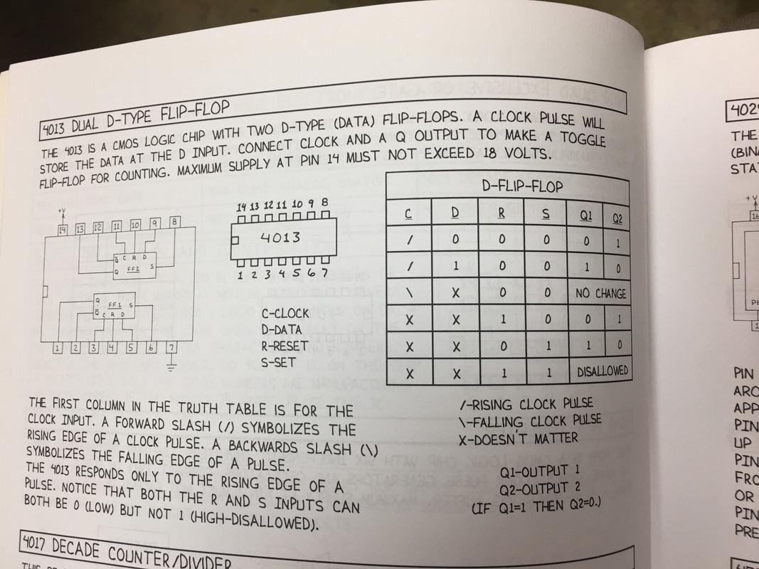
which, as I understand it, on the rising edge of a clock pulse Q1 gets set when D is set.  (By the way, why does he use Q1 and Q2 in the truth table and Q and ~Q (I don't know how to write a Q with a line over it) in the schematic??).  He presents a basic flip flop circuit to demonstrate this :

image

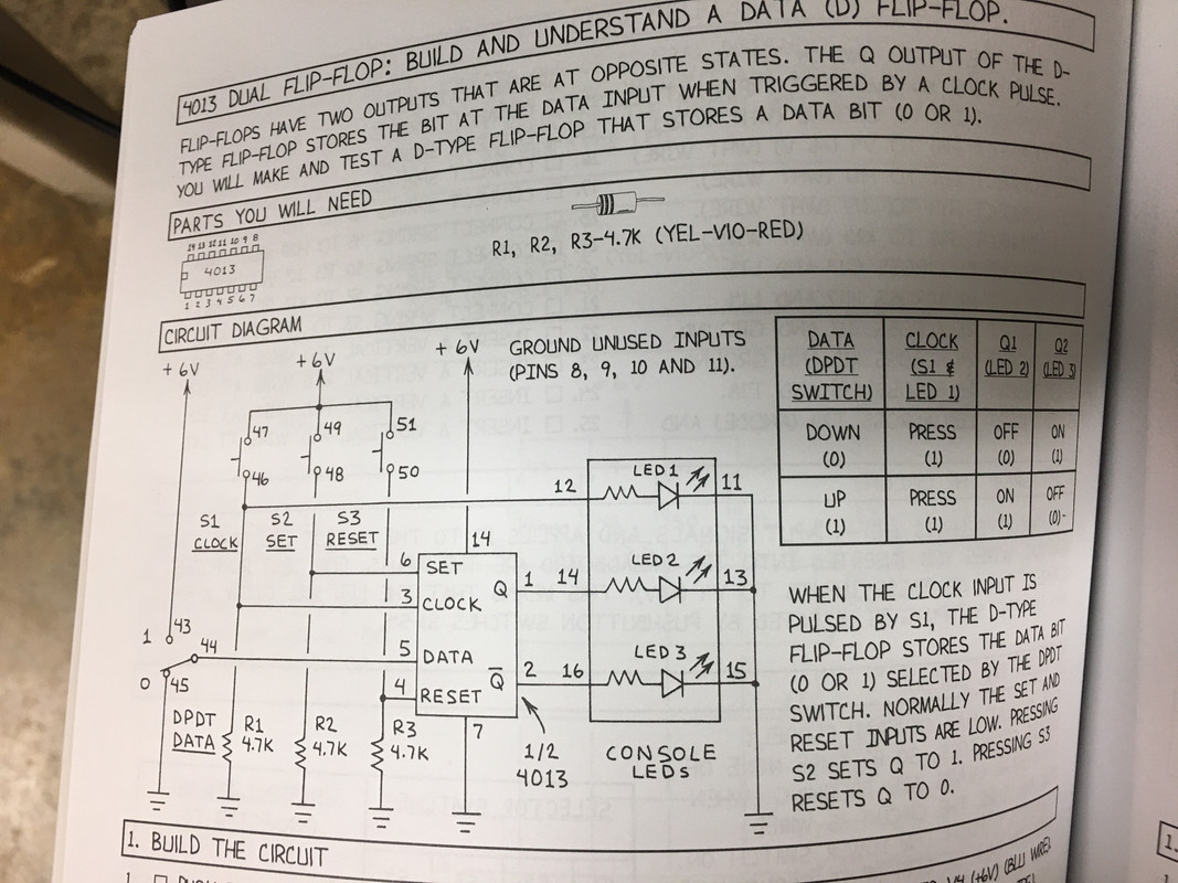
Ok I get when you set D in this circuit with the toggle switch manually, Q1 gets set high (1) with the rising clock pulse!


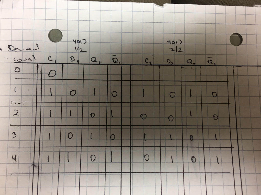
Now the circuit I am working on:

image

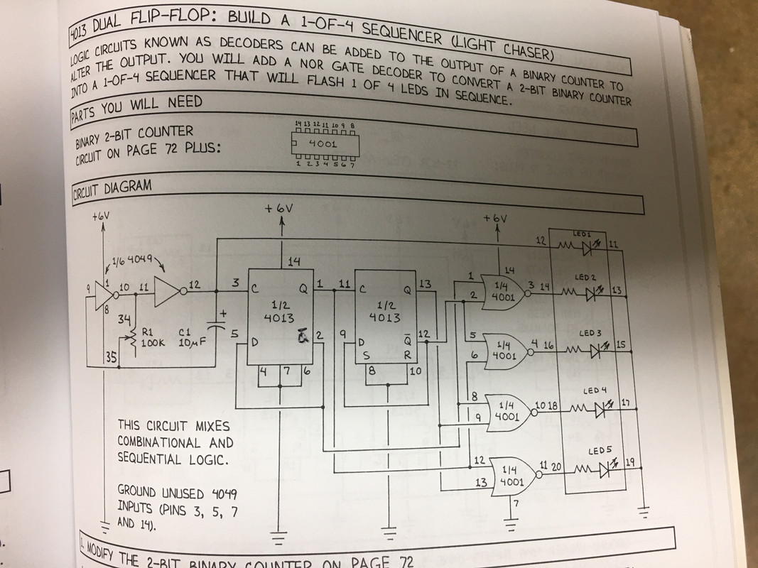
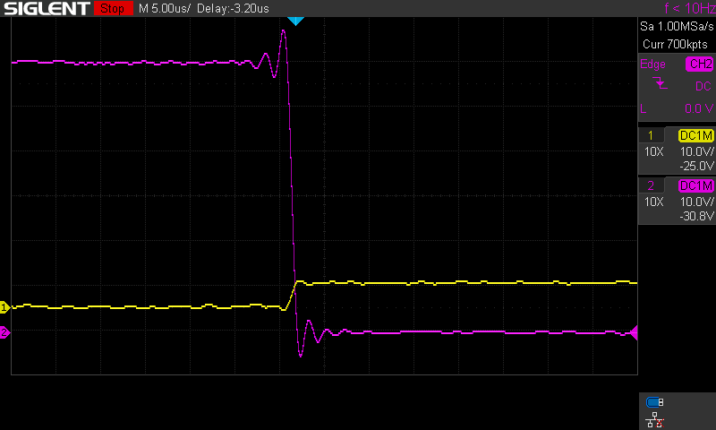
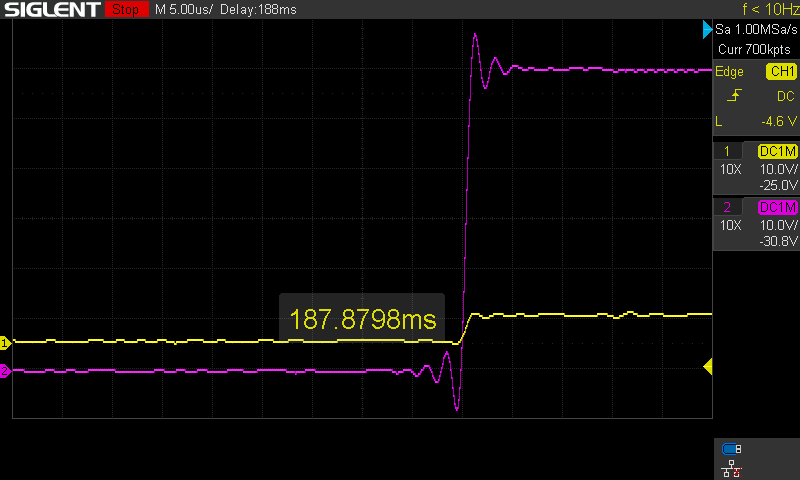
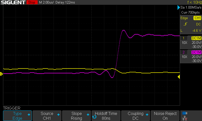
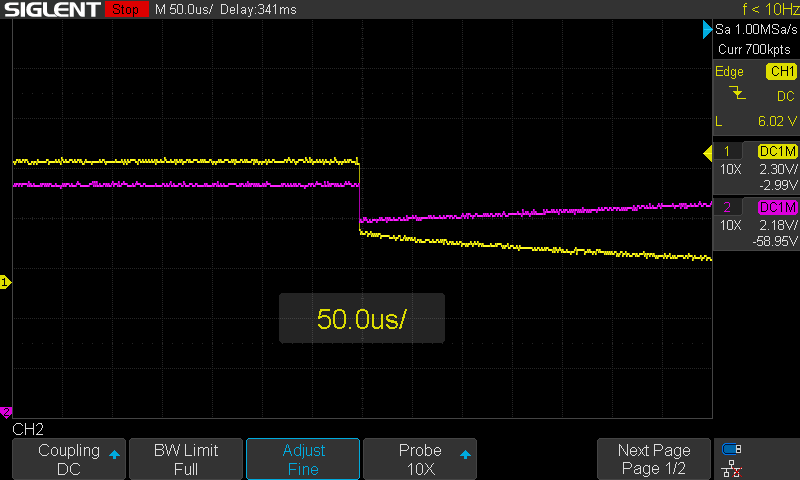
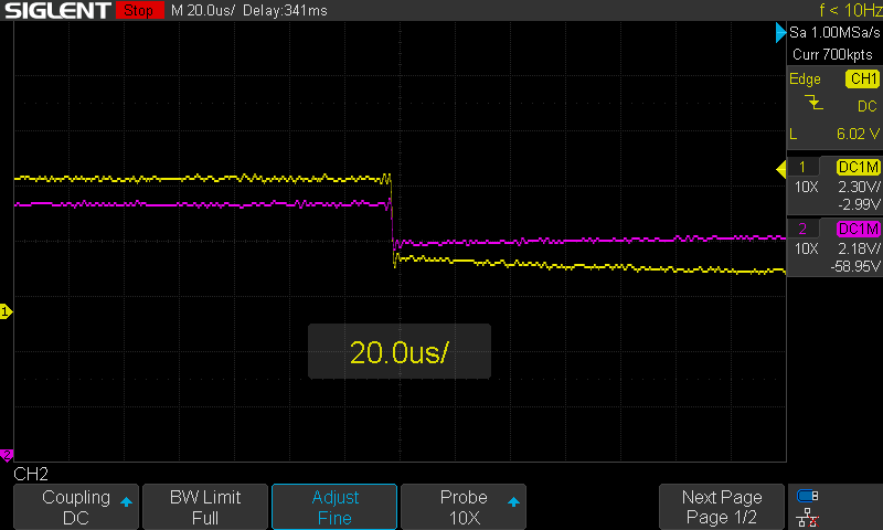
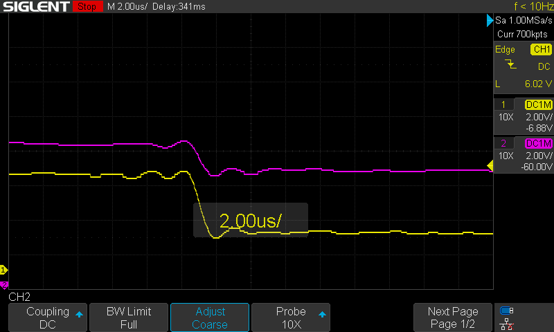
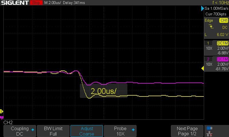
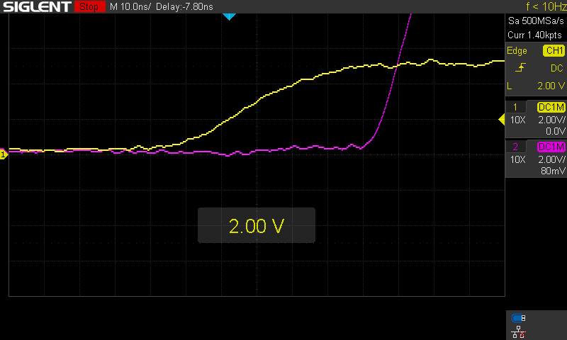
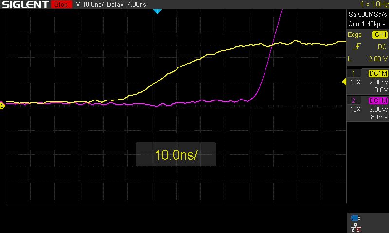
The circuit works as it should, lighting up LED's 1,2,3,4 in sequence.  Ok.  However, when I put a logic probe on pin 5 of the 4013 (D1) with the rising clock pulse starting from 0, D1 is 0 (low) but Q1 is 1 (high). I don't understand why Q1 is set when D1 is low.  Here is the truth table I came up with but it seems to me from the truth table in the image at the top of this post, on rising clock pulse when D1 is 0, ~Q should get set to 1 (high).  I feel like I am missing the sequence of how the outputs get changed but I don't know what...  Help!


image


Thanks!

Robert Opalko


Message was edited by: Robert Opalko


Message was edited by: Robert Opalko

  • Sign in to reply
  • Cancel

Top Replies

  • wolfgangfriedrich
    wolfgangfriedrich over 4 years ago +7 verified
    The short answer is, that the ~Q output (pin2) is connected to the D input (pin5). When the rising edge happens and after the propagation delay of the flipflop the outputs toggle according to the D input…
  • gdstew
    gdstew over 4 years ago in reply to opalko +6 suggested
    Propagation delay, the amount of time an output (Q or ~Q) takes to change after a change in an input (D and clock) for 4000 series ICs is measured in 10s to 100s of nanoseconds depending on the operating…
  • dougw
    dougw over 4 years ago in reply to opalko +6 suggested
    As wolfgangfriedrich points out the FF is operating as it should. When the clock rising edge occurs whatever is at D gets latched to Q. In this case /Q gets latched as the inverse of Q, and it is connected…
Parents
  • wolfgangfriedrich
    0 wolfgangfriedrich over 4 years ago

    The short answer is, that the ~Q output (pin2) is connected to the D input (pin5). When the rising edge happens and after the propagation delay of the flipflop the outputs toggle according to the D input. When D is high, Q goes high and ~Q goes low, which loops back to the D input.

    The logic probe would not show this relationship as the prop delay is only some nanoseconds.

    The long answer would require a timing diagram.

    If you have an oscilloscope, look at the clock, D and Q,~Q signals and trigger on the clock.

    - W.

    • Cancel
    • Vote Up +7 Vote Down
    • Sign in to reply
    • Verify Answer
    • Reject Answer
    • Cancel
  • opalko
    0 opalko over 4 years ago in reply to wolfgangfriedrich

    So D is going high before Q is getting set and I can't see that with the logic probe? If that is the case, is the truth table I constructed incorrect then?

    • Cancel
    • Vote Up +3 Vote Down
    • Sign in to reply
    • Verify Answer
    • Cancel
  • gdstew
    0 gdstew over 4 years ago in reply to fmilburn

    Back when I were just a lad there were things called magazines. Two of my favorites were Popular Electronics and Radio Electronics which always had more than a few do it yourself projects in every issue. Forrest Mims wrote

    DIY articles for both if I remember correctly and he always had interesting projects. The Intel 8008 based MARK 8 kit, which was in an article in the July 1974 issue of Radio Electronics, was what got me interested enough to

    start taking electronics courses in a local community collage and started my 35+ years career and hobby in electronics. Sadly both of these magazines are long, long gone. Luckily, Forrest is still with us.

    • Cancel
    • Vote Up +2 Vote Down
    • Sign in to reply
    • Verify Answer
    • Cancel
  • opalko
    0 opalko over 4 years ago in reply to wolfgangfriedrich

    (Yes, as fmilburn said, the entire book is written this way, as are the other ones I have seen.. Getting Started in Electronics, Mini Notebooks etc.  As for explaining it in the next chapter, well,.. Forrest doesn't explain the circuits much, if at all. It is left to the reader to build the circuit and figure out what is going on, which is what led me here!!!)


    With that being said, I should explain what I was trying do. Rather than look at the blinky lights go on 1,2,3,4  - say "neat" and move on to the next project I was trying to figure out how the 4001 quad NOR gate was getting the signals to turn the LED's on in that sequence.  So I was trying to reverse engineer the circuit back to the truth table level and the results didn't match with what Mims shows in this pic:

    image

    image


    since wolfgangfriedrich said my TT was correct, I am still lost, lol! So is Mims TT incomplete as well?  (Don't even get me started on understanding the 4013 changes in the second part 2/2 with clock and Q2 and ~Q2...)


    I will add some scope screen captures I took after you suggested using scope instead of logic probe. I must not have captured or I don't know what I am looking for as it looks to me like the clock - Q - ~Q  - D all change at the same time; I would have thought one would precede the others.  I should make clear I am a complete novice with using an oscilloscope, and my cheapee Siglent 1202X-E may not be enough to measure what I need to see.


    Pic 1: Yellow is clock signal, Pink is Q

    image

    Pic2:  Yellow is clock signal, pink is ~Q

    image

    Pic 3: Yellow is D, pink is Q

    image

    • Cancel
    • Vote Up 0 Vote Down
    • Sign in to reply
    • Verify Answer
    • Reject Answer
    • Cancel
  • gdstew
    0 gdstew over 4 years ago in reply to opalko

    At 6V you are going to have to sample at 100ns or less to see a difference, probably 50ns minimum, 20ns to get a really good look. Also you should trigger on the high to low clock transition.

    In Pics 1  and 3 you are triggering on the data.

    • Cancel
    • Vote Up +1 Vote Down
    • Sign in to reply
    • Verify Answer
    • Reject Answer
    • Cancel
  • opalko
    0 opalko over 4 years ago in reply to gdstew

    Ok, let me try that again. Stay tuned.

    • Cancel
    • Vote Up 0 Vote Down
    • Sign in to reply
    • Verify Answer
    • Cancel
  • opalko
    0 opalko over 4 years ago in reply to opalko

    Ok, clock yellow, triggered on falling edge. Pink is D / ~Q. 500ns is the limit on this scope.....

    image

    image

    image

    image

    image

    • Cancel
    • Vote Up 0 Vote Down
    • Sign in to reply
    • Verify Answer
    • Cancel
  • dougw
    0 dougw over 4 years ago in reply to opalko

    Can you show The rising edge of the clock and the D input at maximum time resolution?

    When the clock edge is detected at about 2 V the value of D gets latched to Q.

    If D changes after that, and it will because /Q will change, it will not change Q.

    You want to look at the voltage at D when the clock is first recognized as going high.

    • Cancel
    • Vote Up +1 Vote Down
    • Sign in to reply
    • Verify Answer
    • Reject Answer
    • Cancel
  • opalko
    0 opalko over 4 years ago in reply to dougw

    Ok I hope this is correct. Yellow clock, pink D.  I have a long way to go learning how to use my scope image

    • Cancel
    • Vote Up 0 Vote Down
    • Sign in to reply
    • Verify Answer
    • Cancel
  • opalko
    0 opalko over 4 years ago in reply to opalko

    If nothing else I am learning to use my scope better (I think). I was wrong about the limit, here is 10ns... I haven’t figured out why I don’t see D climbing when clock is at 2V; I know I still have scope settings wrong somewhere..

    Thank you for the answers and putting up with my ignorance on this stuff!

    image

    image

    • Cancel
    • Vote Up +1 Vote Down
    • Sign in to reply
    • Verify Answer
    • Cancel
  • dougw
    0 dougw over 4 years ago in reply to opalko

    That is a good scope shot. It shows that D is stable and low when the clock goes high.

    This latches low on Q and high on /Q.

    When /Q goes high, D goes high, because they are connected.

    Because there is no rising clock edge after D goes high, Q stays low.

    The delay between when the clock goes high and when D goes high is the propagation delay through the FF.


    If you capture what happens when D is high and a rising clock happens, D should stay high until after the clock goes high and then go low after about the same propagation delay..

    • Cancel
    • Vote Up +1 Vote Down
    • Sign in to reply
    • Verify Answer
    • Reject Answer
    • Cancel
  • gdstew
    0 gdstew over 4 years ago in reply to opalko

    I've been busy for a while and have some catching up to do here. I don't know how I messed this up but I should have said the low to high clock transition if you want to see the timing relationship between

    the clock pulse and the Q or ~Q output. That is the clock edge used to clock in what is on the D input. My bad! Looking at some of the new scope traces you can clearly see the differences in the signal

    timing so you are on the right track. If switch the D scope trace to the Q output you should be able to see the propagation delay from the rising clock edge to the Q output change. One thing that Doug didn't

    get quite right is the clock threshold voltage needed to clock in the data. On CMOS ICs like the 4013 (and 74HC series) this voltage is higher than ~2V which is the threshold for TTL compatible ICs. The spec

    sheet for the 4013 says 3.5V is the minimum for a 5V power supply so I'm going to guess it needs to be around 3.75 -  4V min. for the 6V supply shown in the book schematics.


    Ignorance is easily fixed by learning and you are clearly making an effort to learn. It really helps that you have the tools to dig deeper when you need to. My only problem here is that I have to attempt to explain

    multifaceted electronic concepts in writing. And there are very few circuits which do not require understanding multiple electronic concepts. For me at least it is much easier to do this with a back and forth

    conversation with a white board close by just in case. Conversation also usually allows me to catch my mistakes when or at least shortly after I make them instead of hours later (ouch, that one hurt).

    • Cancel
    • Vote Up +2 Vote Down
    • Sign in to reply
    • Verify Answer
    • Reject Answer
    • Cancel
Reply
  • gdstew
    0 gdstew over 4 years ago in reply to opalko

    I've been busy for a while and have some catching up to do here. I don't know how I messed this up but I should have said the low to high clock transition if you want to see the timing relationship between

    the clock pulse and the Q or ~Q output. That is the clock edge used to clock in what is on the D input. My bad! Looking at some of the new scope traces you can clearly see the differences in the signal

    timing so you are on the right track. If switch the D scope trace to the Q output you should be able to see the propagation delay from the rising clock edge to the Q output change. One thing that Doug didn't

    get quite right is the clock threshold voltage needed to clock in the data. On CMOS ICs like the 4013 (and 74HC series) this voltage is higher than ~2V which is the threshold for TTL compatible ICs. The spec

    sheet for the 4013 says 3.5V is the minimum for a 5V power supply so I'm going to guess it needs to be around 3.75 -  4V min. for the 6V supply shown in the book schematics.


    Ignorance is easily fixed by learning and you are clearly making an effort to learn. It really helps that you have the tools to dig deeper when you need to. My only problem here is that I have to attempt to explain

    multifaceted electronic concepts in writing. And there are very few circuits which do not require understanding multiple electronic concepts. For me at least it is much easier to do this with a back and forth

    conversation with a white board close by just in case. Conversation also usually allows me to catch my mistakes when or at least shortly after I make them instead of hours later (ouch, that one hurt).

    • Cancel
    • Vote Up +2 Vote Down
    • Sign in to reply
    • Verify Answer
    • Reject Answer
    • Cancel
Children
  • opalko
    0 opalko over 4 years ago in reply to gdstew

    No worries -I am thankful to have folks take the time to reply with answers and explanations!

    • Cancel
    • Vote Up 0 Vote Down
    • Sign in to reply
    • Verify Answer
    • Cancel
element14 Community

element14 is the first online community specifically for engineers. Connect with your peers and get expert answers to your questions.

  • Members
  • Learn
  • Technologies
  • Challenges & Projects
  • Products
  • Store
  • About Us
  • Feedback & Support
  • FAQs
  • Terms of Use
  • Privacy Policy
  • Legal and Copyright Notices
  • Sitemap
  • Cookies

An Avnet Company © 2025 Premier Farnell Limited. All Rights Reserved.

Premier Farnell Ltd, registered in England and Wales (no 00876412), registered office: Farnell House, Forge Lane, Leeds LS12 2NE.

ICP 备案号 10220084.

Follow element14

  • X
  • Facebook
  • linkedin
  • YouTube