Introduction
This is the first blog about my project for the 7 Ways to Leave Your Spartan-6. Here we'll look at how I have put everything together and run a simple test to see if everything is working. The topic of making a polarimeter might seem useless but (at least in my opinion) will provide a decent amount of information about "synchronous" sampling, digital signal processing, etc. There is also a decent amount of code, that can be reused for other projects. Before going any further let's take a quick look at what a polarimeter is and how it works. If you want to know more about this project take a look at the GitHub repo. All of the described Verilog code can be found here, firmware files are here and the Vivado files are here.

As the name suggests a polarimeter is a device used to measure the polarization of light. It's mostly used for scientific experiments, but it can be used in technological applications. For example, it can be used when coupling light to certain optical fibres which are sensitive to light polarization. It is important to note we're not just talking about linear polarization.
We can measure the polarization of light by sending it through a Quarter-waveplate (QWP) followed by a linear polarizer and then measuring the intensity of transmitted light. We then have to sample the intensity at different rotation angles of the QWP. Using some math we can then find the parameters of the light polarization. A much better description can be found here under the operation tab.
As mentioned before, we'll mostly look at how everything fits together as well as a bit of code to check whether everything works as it should.
Hardware - Electronics
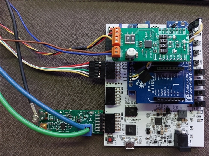
This device consists of two parts the (analog) sensor, where the light gets sampled, and the (digital) electronics. In the middle of the electronics is the Arty S7-25. For analogue to digital conversion, I have used an Analog Devices EVAL-AD7983-PMDZ module connected to the JA PMOD header on the Arty. Since I'm using a brushless dc motor (BLDC), I'll have to use a BLDC motor controller. I have chosen the Mikroelektronika Brushless 7 click along with the Arduino Uno click adapter. The Arduino Uno shield adapter had to be modified such that pins A2-A5 do not connect to the Arty. SCL and SDA on the Arty also had to be connected to A5 and A4 on the adapter respectively. This can be seen in the image, where the yellow and white wires run across the shield adapter.
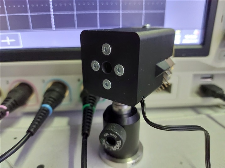
Hardware - Sensor
As mentioned before, the sensor consists of a QWP and a linear polarizer. At one end there is an amplified photodetector, whose signal is measured by the ADC. To rotate the QWP I'm using a BLDC motor with a hollow shaft (so the light can pass through it). To measure the angle of the QWP, I am using a 3-channel quadrature encoder with 512 counts per revolution. This allows us to "divide" one single revolution into 2048 steps/counts. Usage of a 3-channel quadrature encoder is important so that we can find a "zero" position of a sensor, hence we can find the absolute position/rotation. The encoder is connected to the JC PMOD header on the Arty. The BLDC connects directly to the Brushless 7 click and is supplied with +12V. For more information refer to the GitHub repo mentioned in the introduction.
FPGA
Now that we have finally covered some basics of how everything is put together, we can take a look at how this device "ticks". I'm using two "independent" modules. The first one communicates with the ADC and the second one receives data from the quadrature encoder. For testing purposes, I have also written a third module which we'll cover a little bit later.
Quadrature encoder
I have used a 3-channel quadrature encoder. The outputs A and B are simply two "clocks" where one is delayed by a quarter of a cycle. The third output (I) sends out a pulse once per full revolution. To keep things short I would suggest looking at this tutorial/guide. I have used their code as a reference and modified it such that when output-I is high, the count will be set to 0 when the next state change of A or B happens. The module also has additional outputs such as dir, which might come in handy at some later stage.
`timescale 1ns / 1ps

module Encoder_decoder(
    input           clk_i,      //Main FPGA Clock input
    input           nres_i,     //Reset input
    input           A_i,        //Encoder A signal input
    input           B_i,        //Encoder B signal input
    input           I_i,        //Encoder I signal input (optional, used to determine absolute position)
    output  [10:0]  cnt_o,      //Count Output, width should be adjusted so the highest cnt_o value is equal or greater to CPR of the encoder
    output          dir_o       //Direction signal output, HIGH if cnt is increasing, LOW if cnt is decreasing


);
    //REGISTERS
    reg         A_del;      //A signal delayed for 1 clock cycle
    reg         B_del;      //B signal delayed for 1 clock cycle
    reg [10:0]  cnt;        //Stores the encoder count value
    reg         I_hold;     //Tells us whether we crossed the "zero" position recently

    //WIRES
    wire cnt_en     = A_i ^ A_del ^ B_i ^ B_del;
    wire cnt_dir    = A_i ^ B_del;

    //ASSIGN STATEMENTS
    assign cnt_o = cnt;
    assign dir_o = cnt_dir;

    //INITIAL STATEMENTS
    initial cnt <= 0;
    initial I_hold <=0;


    always @(posedge clk_i)
    begin
        if(~nres_i)
            begin
                cnt <= 0;       //Reset the count register
                I_hold <= 0;    //Reset the I_hold register (we can assume that absolute position is unknown at this point)

            end
        else
            begin
                //Get the delayed A and B signal
                A_del <= A_i;
                B_del <= B_i;
                if(I_i && (cnt != 0))
                begin
                    I_hold<= 1; //If I input is high, and count is nonzero, we can set count to zero at the next encoder step
                end

                if(cnt_en)
                begin

                    begin
                        if(cnt_dir)
                            begin
                                cnt <= I_hold ? 0 : cnt + 1;    //If I_hold is HIGH set the count to 0, otherwise increment it by 1
                            end
                        else
                            begin
                                cnt <= I_hold ? 0 : cnt - 1;     //If I_hold is HIGH set the count to 0, otherwise decrement it by 1
                            end

                    end

                    I_hold <= 0;    //Reset the I_hold to LOW
                end

            end
    end

endmodule
When using the encoder, I have noticed that the output state changes are noisy and they have to be debounced. This was solved by adding some additional code to the design. This module will tell us the absolute angle of the QWP with the precision of 360°/2048 ~ 0.18°.
ADC
The code used to communicate with the AD7983 ADC is probably the most complicated piece of code used in this blog post since it works across two clock domains. The communication happens across 3 signals: CNV, SDO and SCK. If the ADC is left alone, it will constantly stay in acquisition mode. Whenever CNV is set to high, it will switch into conversion mode. Conversion lasts about 300-500ns. After the conversion is done, the data can be sent to FPGA. We can do this by applying a clock signal to SCK for 16 cycles. On every cycle, the ADC will write one bit to SDO from bit 15 to bit 0. During this time CNV has to be held high. When we have acquired data we can pull CNV low and now we're able to repeat the whole process.
This seems simple enough. Issues arise when the clock applied to SCK is not the same as the main clock used in the FPGA. For example, I am using a 100MHz clock across the FPGA but am applying a 30MHz clock to the ADC. Therefore we'll have to use a simple state machine which will follow the state of the ADC.
I have used the code supplied by Analog devices. The issue with this code is that it periodically reads from the ADC. Instead, I need to read (trigger) the ADC based on the output of the quadrature encoder. Another issue is that I needed a different data-ready signal. Hence I have modified it to my needs.
`timescale 1ns/1ns //Use a timescale that is best for simulation.

//This is a modified RTL code taken from https://wiki.analog.com/resources/fpga/altera/bemicro/ad7983
//The modification is such that we can trigger the AD7983 chip externally, as well as the behaviour of data ready output
//NOTE: This has not been optimized to work as optimaly as it could. For current requirements it seems completely adequate
module AD7983_driver

//----------- Ports Declarations -----------------------------------------------
(
    //clock and reset signals
    input               fpga_clk_i, //system clock
    input               adc_clk_i, //clock to be applied to ADC to read the conversions results
    input               reset_n_i, //active low reset signal

    //IP control and data interface
    output     [15:0]   data_o, //data read from the ADC
    output reg          data_rd_ready_o, //when set to high the data read from the ADC is available on the data_o bus

    //ADC control and data interface
    input               adc_sdo, //ADC SDO signal
    output              adc_sclk_o, //ADC serial clock
    output              adc_cnv_o, //ADC CNV signal
    input               trigg_i
);

    //------------------------------------------------------------------------------
    //----------- Registers Declarations -------------------------------------------
    //------------------------------------------------------------------------------
    reg [ 3:0]  adc_state; //current state for the ADC control state machine
    reg [ 3:0]  adc_next_state; //next state for the ADC control state machine
    reg [ 3:0]  adc_state_m1; //current state for the ADC control state machine in the ADC clock domain

    reg [ 6:0]  adc_tcnv_cnt; //counts the number of FPGA clock cycles to determine when an ADC conversion is complete
    reg [ 4:0]  sclk_clk_cnt; //counts the number of clocks applied to the ADC to read the conversion result

    reg			adc_clk_en; //gating signal for the clock sent to the ADC
    reg         adc_cnv_s; //internal signal used to hold the state of the ADC CNV signal
    reg [15:0]  adc_data_s; //interal register used to store the data read from the ADC
    reg         tg_prev_state;  //Used to hold the previous trigger_i value


    //------------------------------------------------------------------------------
    //----------- Wires Declarations -----------------------------------------------
    //------------------------------------------------------------------------------
    wire        adc_sclk_s; //internal signal for the clock sent to the ADC

    //------------------------------------------------------------------------------
    //----------- Local Parameters -------------------------------------------------
    //------------------------------------------------------------------------------
    //ADC states
    parameter ADC_IDLE_STATE            = 4'b0001;
    parameter ADC_START_CNV_STATE       = 4'b0010;
    parameter ADC_END_CNV_STATE         = 4'b0100;
    parameter ADC_READ_CNV_RESULT       = 4'b1000;

    //ADC timing
    parameter real FPGA_CLOCK_FREQ  = 100; //FPGA clock frequency [MHz]
    parameter real ADC_CONV_TIME    = 0.50; //conversion time (Tcnvh) [us]
    parameter [6:0] ADC_CNV_CNT     = FPGA_CLOCK_FREQ * ADC_CONV_TIME;

    //ADC serial clock periods
    parameter ADC_SCLK_PERIODS  = 5'd15; //number of clocks to be sent to the ADC to read the conversion result
    parameter DATA_READY_CNT = 3;

    //------------------------------------------------------------------------------
    //----------- Assign/Always Blocks ---------------------------------------------
    //------------------------------------------------------------------------------

    assign adc_cnv_o      = adc_cnv_s;
    assign adc_sclk_s	  = adc_clk_i & adc_clk_en;
    assign adc_sclk_o     = adc_sclk_s;

    assign data_o         = adc_data_s;


    //update the ADC timing counters
    always @(posedge fpga_clk_i)
    begin
        if(reset_n_i == 1'b0)
            begin

                adc_tcnv_cnt    <= ADC_CNV_CNT;
            end
        else
            begin
                //Data is ready only during the IDLE state, other states indicate the process of acquiring data.
                data_rd_ready_o <= (adc_state == ADC_IDLE_STATE) ? 1 : 0;    //Delay data ready output by one clock cycle to prevent any clock domain bugs.
                tg_prev_state <= trigg_i;

                if(adc_state == ADC_START_CNV_STATE)
                    begin
                        adc_tcnv_cnt <= adc_tcnv_cnt - 1;
                    end
                else
                    begin
                        adc_tcnv_cnt <= ADC_CNV_CNT;
                    end


            end
    end

    //read data from the ADC
    always @(negedge adc_clk_i)
    begin
        if(adc_clk_en == 1'b1)
            begin
                adc_data_s   <= {adc_data_s[14:0], adc_sdo};
                sclk_clk_cnt <= sclk_clk_cnt - 1;
            end
        else
            begin
                sclk_clk_cnt <= ADC_SCLK_PERIODS;
            end
    end

    //determine when the ADC clock is valid to be sent to the ADC
    always @(negedge adc_clk_i)
    begin
        adc_state_m1 <= adc_state;
        adc_clk_en   <= ((adc_state_m1 == ADC_END_CNV_STATE) || (adc_state_m1 == ADC_READ_CNV_RESULT) && (sclk_clk_cnt != 0)) ? 1'b1 : 1'b0;
    end

    //update the ADC current state and the control signals
    always @(posedge fpga_clk_i)
    begin
        if(~reset_n_i)
            begin
                adc_state <= ADC_IDLE_STATE;
            end
        else
            begin
                adc_state <= adc_next_state;
                case (adc_state)
                    ADC_IDLE_STATE:
                    begin
                        adc_cnv_s       <= 1'b0;

                    end
                    ADC_START_CNV_STATE:
                    begin
                        adc_cnv_s       <= 1'b1;

                    end
                    ADC_END_CNV_STATE:
                    begin
                        adc_cnv_s       <= 1'b0;

                    end
                    ADC_READ_CNV_RESULT:
                    begin
                        adc_cnv_s       <= 1'b0;

                    end
                endcase
            end
    end

    //ADC State machine scheduling. State progression is as follows ADC_IDLE_STATE -> ADC_START_CNV_STATE -> ADC_END_CNV_STATE -> ADC_READ_CNV_RESULT -> ADC_IDLE_STATE
    always @(adc_state, trigg_i, adc_tcnv_cnt, sclk_clk_cnt)
    begin
        adc_next_state <= adc_state;
        case (adc_state)
            ADC_IDLE_STATE:
            begin
                if(tg_prev_state != trigg_i)    //Change to ADC_START_CNV if the value of the trigger input has changed
                begin
                    adc_next_state <= ADC_START_CNV_STATE;

                end
            end
            ADC_START_CNV_STATE:
            begin
                if(adc_tcnv_cnt == 0)           //Transition to next state if enough time has passed
                begin
                    adc_next_state <= ADC_END_CNV_STATE;
                end
            end
            ADC_END_CNV_STATE:
            begin
                adc_next_state <= ADC_READ_CNV_RESULT;
            end
            ADC_READ_CNV_RESULT:            //Transition to IDLE state if enough SCLK cycles have passed
            begin
                if(sclk_clk_cnt == 1)
                begin
                    adc_next_state <= ADC_IDLE_STATE;
                end
            end
            default:
            begin
                adc_next_state <= ADC_IDLE_STATE;
            end
        endcase

    end


endmodule
This allows me to have a trigger input, which will start the conversion whenever the state of trigg_i changes. The output data_rd_ready_o will be set high whenever data is available, and will immediately go low whenever a new ADC reading has started.
Since I want to trigger the ADC when the encoder changes its state, I have used the debounced A and B signals fed into an XOR gate and routed the output to the ADC trigger input. Equivalently I could route the least significant bit of the encoder count to the trigger input. In the following image, we can see how both the quadrature encoder and the ADC behave (the most significant bit is not connected to the logic analyzer, hence the count is capped to 1023. In the FPGA it still goes to 2047).

We can see that when the encoder count changes, the data_ready signal is set to low for a short period, after which it goes back to high signalling that we have correct data on the data bus of the ADC module.
Putting things together
To test whether everything works as it should, we can store the data from the ADC to on-chip block memory (BRAM), and then read it over the serial port. For this, we'll need a "data mover". It was written such that it starts when it receives a pulse (should not be longer than the time required for one rotation). After which it waits for the desired encoder count and data_ready on the ADC module. When both conditions are met it sets the output registers such that 16 bits of ADC data are written to the BRAM into the address equal to the current encoder count. The desired encoder count is also increased by 1. When it completes a full rotation the module returns to an idle state. The BRAM is configured to be interfaced through the AXI BRAM controller, hence it is 32 bits wide. Since we have 2048 encoder positions, the BRAM should be 2048 deep.
`timescale 1ns / 1ps

module sampling_controller(
    //Common signals
    input           fpga_clk_i, //Main FPGA clock
    input           reset_n_i, //Main FPGA nreset
    output reg      data_ready_o, //Data Ready output, data_ready_o will be pulled high, when data is sampled on for every encoder count
    input           trigger_i, //Trigger input, data will be sampled after trigger_i is pulled HIGH
    output reg      idle_o,

    //BLOCK MEMORY GENERATOR signals
    output reg  [31:0]  bram_addr, //BRAM address
    output          bram_clk, //BRAM clock
    output reg  [31:0]  bram_wrdata, //BRAM write data
    input   [31:0]  bram_rddata, //BRAM read data
    output reg      bram_en, //BRAM clock enable
    output reg  [3:0]   bram_we, //BRAM write enable

    //ADC signals
    input           adc_data_ready_i, //ADC data ready
    input   [15:0]  adc_data_1, //ADC data
    input   [15:0]  adc_data_2, //ADC data, can be used to connect the second ADC, for example could be used in dynamic load balancer

    //Encoder signals
    input   [10:0]  enc_cnt_i //Encoder count

);
    reg     [10:0]  cpos;   //Internal position count


    initial cpos = 0;
    initial idle_o = 1;
    initial data_ready_o = 0;

    assign bram_clk = fpga_clk_i;


    always @(posedge fpga_clk_i)
    begin

        if(~reset_n_i)
            begin
                cpos <= 0;
                idle_o <= 1;
               data_ready_o  <= 0;
            end
        else
            begin
                if(idle_o) //If idle and trigger_i are HIGH, we will start sampling for one single revolution
                    begin
                        if(trigger_i)
                        begin
                            idle_o <= 0;
                            cpos <= 0;
                            data_ready_o  <= 0;
                        end
                    end
                else
                    begin
                        if(cpos == enc_cnt_i) //If we are in desired position
                            begin
                                if(adc_data_ready_i) //If we have ADC data
                                begin
                                    bram_addr <= {19'b0, cpos,2'b0}; //Set BRAM address to "current encoder position". BRAM width is 32, therefore the addresses are shifted by 2 bits to the left. Address widht is 32 so well also pad the output with 19 0s
                                    bram_wrdata <= {adc_data_2,adc_data_1}; //Write current adc reading to BRAM
                                    //bram_wrdata <= {21'b0, cpos}; //Used for debugging, simply writes to registers their addresses
                                    bram_we <= 4'b1111; //Set write enable to high to indicate the write operation
                                    cpos <= cpos + 1; //Advance to next position
                                    bram_en <= 1;   //Set BRAM enable HIGH
                                    if(cpos == 11'd2047) //2047 is the last encoder count. If it's reached we can now set the state to IDLE, and signal that the data is ready
                                    begin
                                        idle_o <= 1;
                                        data_ready_o  <= 1;
                                    end
                                end
                            end
                        else
                            begin
                                bram_we <= 0; //Stop writing to bram even though data should still be correct since it is stored in the register.
                                bram_en <= 0;
                                bram_wrdata <= 0;
                            end
                    end
            end

    end
endmodule
Microblaze and peripherals
Since we'll have to configure the BLDC controller over I2c and somehow transmit the data that was read, we'll use the Microblaze microprocessor IP. It is left in the default configuration and the necessary peripherals are generated by block automation. Lastly, we'll have to add AXI Uart to connect to the PC, AXI I2c to talk to the motor controller as well as the AXI BRAM to read the memory. The data_ready from the "data_mover" is connected to bit 1 (zeroth is for uart) of the AXI interrupt. I have set the Baud rate of the uart to 203400. I have also added AXI SPI but was unable to use it as I wanted (will try again in the future). The complete block design is as follows: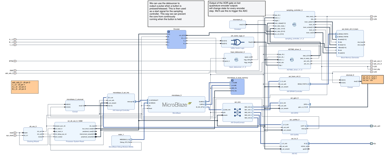
Microblaze firmware
The firmware is very simple. The only things that have to be done are to set up the BLDC controller, UART and interrupts. Finally, the contents of the BRAM should be sent over serial. For BLDC controller configuration, I have written a short library. Most of the parameters were set through trial and error and are yet to be finalised. The library can be found here (the header is located in the parent folder). Finally. the firmware that brings everything together.
//INCLUDES
#include <stdio.h>
#include "platform.h"
#include "xil_printf.h"
#include "xparameters.h"
#include "xintc.h"
#include "xil_exception.h"
#include "xil_io.h"
#include "motor_controller.h"
#include "xiic.h"
#include "xbram.h"

//I2C DEFINES
#define IIC_DEVICE_ID	   	XPAR_IIC_0_DEVICE_ID
#define IIC_BASE_ADDRESS	XPAR_IIC_0_BASEADDR
#define IIC_MOTOR_ADDRESS	0x29

//BRAM DEFINES
#define BRAM_DEVICE_ID		XPAR_AXI_BRAM_CTRL_0_DEVICE_ID
#define BRAM_BASE_ADDR		XPAR_BRAM_0_BASEADDR

//INTERRUPT DEFINES
#define INTC_DEVICE_ID		XPAR_INTC_0_DEVICE_ID
#define DSP_INTERRUPT_CHANNEL 1


//FUNCTIONS
void WriteFromBram(void *CallbackRef);


XBram Bram;
XBram_Config *ConfigPtr;
u32 Bram_low_addr;
u32 Bram_num_addr;
u8	InterruptTriggd = 0;
int main() {
	init_platform();	//Initialize the platform (UART)
	microblaze_enable_interrupts();	//Enable the interrupts
	//NOTE: all non-data Serial writes should have an "I" as the first letter and should be terminated by newline "\t". This allows easy communication between python and Microblaze.
	xil_printf("I: Initializing!\n");
	motor_default_settings(IIC_BASE_ADDRESS, IIC_MOTOR_ADDRESS);	//Configure the motor controller to known usable settings
	motor_configure(IIC_BASE_ADDRESS, IIC_MOTOR_ADDRESS);			//Configure the motor to I2C operation, set number of poles and max RPM
	motor_start_rpm(IIC_BASE_ADDRESS, IIC_MOTOR_ADDRESS, 5);		//Set motor start RPM
	motor_set_speed(IIC_BASE_ADDRESS, IIC_MOTOR_ADDRESS, 400);		//Configure motor setpoint speed (not in rpm e.g. with curren motor setpoint of 400 results in 1440 RPM)
	xil_printf("I: Motor Started!\n");
	xil_printf("I: Configuring Interrupts!\n");


	cleanup_platform();

	u32 Addr;
	//Configure the interrupts
	XIntc_RegisterHandler(XPAR_INTC_0_BASEADDR, DSP_INTERRUPT_CHANNEL, (XInterruptHandler)WriteFromBram, (void *)1);
	XIntc_MasterEnable(XPAR_INTC_0_BASEADDR);
	XIntc_EnableIntr(XPAR_INTC_0_BASEADDR, 0x3);
	xil_printf("I: Configured Interrupts!\n");

	//Main loop
	while(1)
	{
		//If we had a trigger event
		if(InterruptTriggd){
			for (Addr = 0; Addr <2048; Addr++)
				{
							//Print out data for every Bram register. These are 32 bit wide, hence we should step by 4. This can be done through Addr*4 or by bitshifting Addr<<2
							//Data is written as "Address:Data\n". Value of address corresponds to encoder position.
							xil_printf("%i:%i\n",Addr,XBram_ReadReg(BRAM_BASE_ADDR,Addr<<2));
				}
			//Reset the InterruptTriggd flag to stop unnecessarily reading from bram.
			InterruptTriggd = 0;
		}
	}

}

void WriteFromBram(void *CallbackRef)
{
	//Set the InterruptTriggd to 1 to signal, that we have fresh data stored in BRAM.
	InterruptTriggd = 1;

}
How it works
When everything is connected correctly and the FPGA is programmed, the motor should start running. Firstly, four lines of status information should appear on the serial terminal. Then the device will be idle. If the BTN0 is pressed, data will be sampled for a single rotation, after which said data will be sent over serial. To keep things simple I have written a short Python script to read the data and display it in a polar plot as well as a regular XY plot.
from ast import And
from operator import and_
import numpy as np
import serial
import matplotlib.pyplot as plt
import sys
#!/usr/bin/python

#Open serial communication. NOTE: Set port to the port to which the Arty S7 is connected to. Also make sure that the python script is able to access the port (for linux use: sudo chmod 666 /dev/ttyUSB1)
ser = serial.Serial(port = "/dev/ttyUSB1", baudrate = 230400, bytesize = 8, timeout = 2, stopbits = serial.STOPBITS_ONE)

#Close the serial port if it has not yet been closed
if ser.is_open :
    ser.close()

#(Re)open the serial port
ser.open()

#Create an array that will hold x values used for plotting figure 1
xs = np.linspace(0,2047,2048)

#Create an array that will hold angle values used for plotting figure 2 (polar plot -> 2048 values spaced from 0 to 2pi)
thetas = xs*(np.pi/1024)

#Create a buffer array that will hold y (also r for polar plot) values. We'll fill it with data later
data = np.zeros(2048)


plt.ion()

#Setup plot on figure 1 (regular xy plot)
fig1 = plt.figure(1)
ax1 = fig1.add_subplot(111)
line1, = ax1.plot(xs,data, 'r-')
ax1.grid(True)
ax1.set_ylabel('ADC counts')
ax1.set_xlabel('Encoder position')

#Setup plot on figure 2 (polar plot)
fig2 = plt.figure(2)
ax2 = fig2.subplots(subplot_kw = {'projection': 'polar'})
line2, =ax2.plot(thetas, data)
ax2.grid(True)
ax2.set_xlabel('Angle')


#Create a temporary array that will hold the split strings with data
temp = ["",""]

print("Press button BTN0 to sample data for a single rotation")
#Run while both figures are open
while(plt.fignum_exists(1) and plt.fignum_exists(2)):
    #Check whether data is available
    if(ser.in_waiting > 0):
        #Read the line of data
        inputData = ser.readline().decode("ASCII")
        #All non-data starts with "I"
        if(inputData[0] != "I"):
            #Split data into position and value string
            temp = inputData.split(":")
            #Store the value into the correct position in the array
            data[int(temp[0])] = int(temp[1])
    #Data with position of 2047 is the last that is sent out, hence we can now draw/redraw the plots
    if(temp[0]=="2047"):
        #Update figure 1
        line1.set_ydata(data)
        fig1.canvas.draw()
        fig1.canvas.flush_events()
        ax1.set_ylim([0,max(data)+100])
        #Update figure 2
        line2.set_ydata(data)
        fig2.canvas.draw()
        fig2.canvas.flush_events()
        ax2.set_ylim([0,max(data)+100])

#When either of the figures is closed the program should stop running.
#We can close the serial port now.
ser.close()
Results
To test if everything works as it should, I have used polarised laser light sent into the polarimeter sensor. The following plots are the output of the Python script.
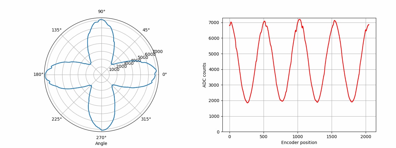
Finally, we can compare the results with the data recorded by an oscilloscope. In the following image the yellow line represents the I output of the encoder and the green line shows the signal on the photodetector.
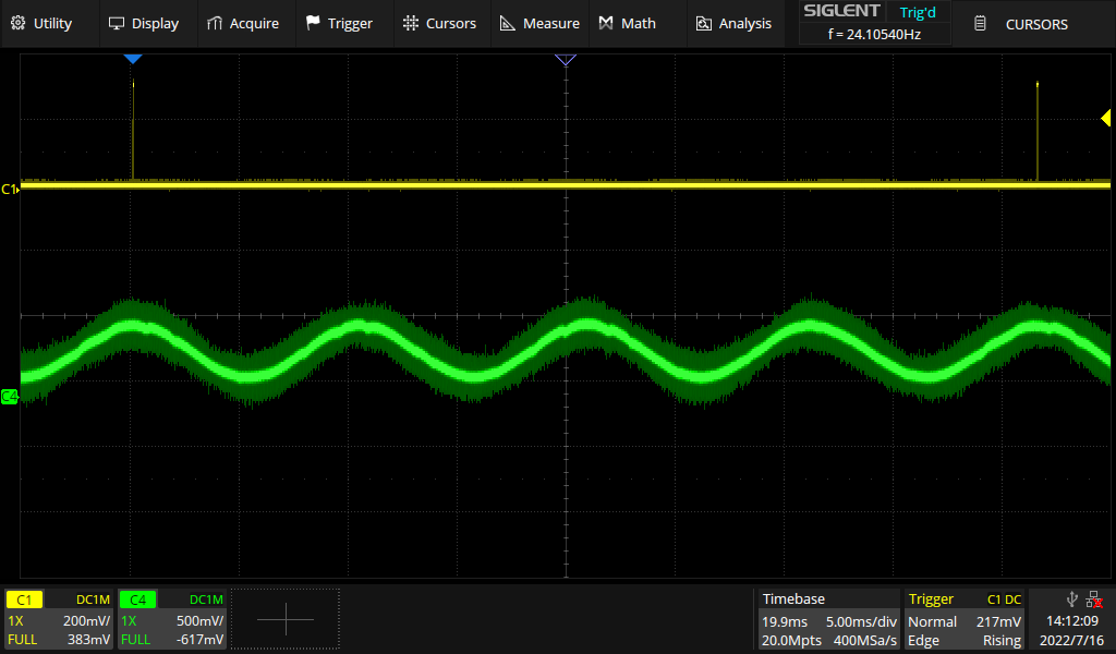
We can see the signals are very similar albeit the data gathered by the FPGA is a lot less noisy. One of the reasons is that the ADC is only sampling when there is no digital activity between the peripherals and the FPGA.
Conclusion
As I have said at the beginning of this post, this is part 1 of 2. In the next post, we'll be looking at implementing a DSP to process the data and send it to a host computer. I'll also try to make a simple measurement using the polarimeter, to test its performance.
But for now, thank you for reading. Please leave a comment if I need to explain something better or if I missed something or even if you have some ideas.
Best regards, Jure Pirman.

