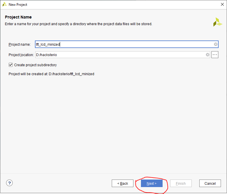
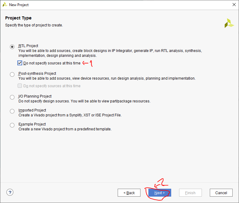
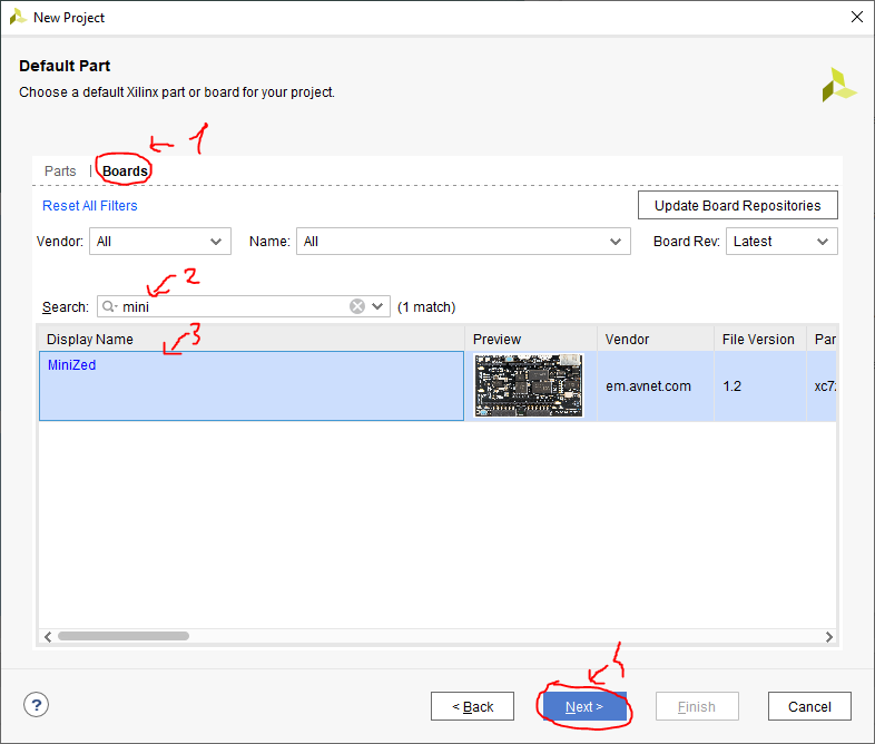
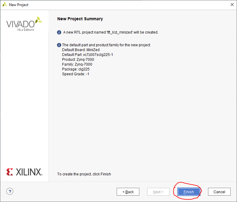
| {gallery}Vivado project creation |
|---|
|
|
|
|
|
|
|
|
|
|
-
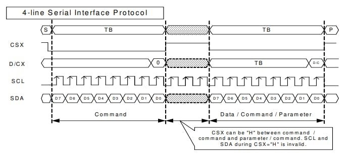
CS - chip select (CSX)
-
RS - register select (D/CX)
-
CLK - spi clock (SCL)
-
MOSI - master output slave input (SDA)
-
When CS is high, all commands and parameters are ignored
-
We are starting the transition by holding CS in low state
-
At the next positive edge of the SCL, the oldest bit - D7 is being sampled, then on the next edge D6 etc...
-
On the last bit of the byte - D0, the driver also samples D/CX signal. Before that, D/CX is ignored.
module spi_4l_8b(
    input [8:0]command_tdata,
    input command_tvalid,
    output reg command_tready,
    output reg spi_cs,
    output reg spi_mosi,
    output spi_rs,
    output spi_clk,
    input clk,
    input reset
);

reg data_locked = 0;
reg [8:0] command = 0;
reg [3:0] command_bit_counter = 7;

assign spi_clk = clk;
assign spi_rs = command[8];

always @(posedge clk) begin
    if (!reset) begin
        data_locked <= 0;
        command <= 0;
        command_tready <= 0;
        command_bit_counter <= 7;
        spi_cs <= 1;
    end else begin
        if (!data_locked) begin: wait_for_transaction
            spi_cs <= 1;
            if (command_tready && command_tvalid) begin
                command <= command_tdata;
                command_tready <= 0;
                data_locked <= 1;
            end else begin
                command_tready <= 1'b1;
            end
        end else begin
            spi_cs <= 0;
            spi_mosi <= command[command_bit_counter];
            if (!command_bit_counter) begin: send_spi_data
                command_bit_counter <= 7;
                data_locked <= 0;
            end else begin
                command_bit_counter <= command_bit_counter - 1;
            end
        end
    end
end

endmodule
module spi_4l_8b_cmd_delay
#(parameter delay_val = 500000)(
    output [8:0]out_command_tdata,
    output out_command_tvalid,
    input out_command_tready,
    input [8:0]in_command_tdata,
    input in_command_tvalid,
    output in_command_tready,
    input clk,
    input reset
);

reg [31:0] delay_counter = 0;
reg lock = 0;

assign out_command_tdata = in_command_tdata;
assign out_command_tvalid = in_command_tvalid && (!lock);
assign in_command_tready = out_command_tready && (!lock);

always @(posedge clk) begin
    if (!reset) begin
        delay_counter <=0;
        lock <= 0;
    end else begin
        if (
           !in_command_tdata[8] && //If incoming data is command
           (in_command_tdata[7:0] != 8'b0010_1100) && //If command is not screen write
           out_command_tready && //If AXI4 transaction
           in_command_tvalid && //passes
           !lock // and IP is not already locked.
        ) begin
            lock <= 1;
            delay_counter <= delay_val;
        end else if (!delay_counter) begin
            lock <= 0;
        end
        if (delay_counter) begin: decrement_delay_counter
            delay_counter <= delay_counter - 1;
        end
    end
end

endmodule
-
First, after reset, initialize LCD with default values.
-
Second, send memory write command to LCD after 240x320 pixels.
-
Third, parse the incoming 8-bit stream into 9-bit SPI commands.
`define ili_NOP             8'h00       // No Operation - NOP
`define ili_SWRESET         8'h01       // Software Reset - SWRESET
`define ili_SLPOUT          8'h11       // Sleep Out
`define ili_GAMSET          8'h26       // Gamma Set
`define ili_DISPOFF         8'h28       // Display OFF
`define ili_DISPON          8'h29       // Display ON
`define ili_CASET           8'h2A       // Column Address Set
`define ili_PASET           8'h2B       // Page (row) Address Set
`define ili_RAMWR           8'h2C       // Memory Write
`define ili_MADCTL          8'h36       // Memory Access Control
`define ili_IDMOFF          8'h38       // Idle Mode OFF
`define ili_IDMON           8'h39       // Idle Mode ON
`define ili_PIXSET          8'h3A       // COLMOD: Pixel Format Set
`define ili_RAMWRCont       8'h3C       // Write Memory Continue
`define ili_FRMCTR1         8'hB1       // Frame Rate Control (In Normal Mode/Full Colors)
`define ili_DISCTRL         8'hB6       // Display Function Control
`define ili_PWCTRL1         8'hC0       // Power Control 1
`define ili_PWCTRL2         8'hC1       // Power Control 2
`define ili_VMCTRL1         8'hC5       // VCOM Control 1
`define ili_VMCTRL2         8'hC7       // VCOM Control 2
`define ili_PGAMCTRL        8'hE0       // Positive Gamma Correction
`define ili_NGAMCTRL        8'hE1       // Negative Gamma Correction
`define ili_PCA             8'hCB       // Power Control A
`define ili_PCB             8'hCF       // Power Control B
`define ili_DTCA_ic         8'hE8       // Driver Timming Control A
`define ili_DTCB            8'hEA       // Driver Timming Control B
`define ili_POSC            8'hED       // Power On Sequence Control
`define ili_E3G             8'hF2       // Enable 3G
`define ili_PRC             8'hF7       // Pump Ratio Control

module spi_4l_8b_fifo
#(parameter MEMORY_LIMIT = 96) // Nb of init commands
(
    input [7:0]in_command_tdata,
    input in_command_tvalid,
    output reg in_command_tready,
    output [8:0]command_tdata,
    output reg command_tvalid,
    input command_tready,
    output reg counter_ce,
    input clk,
    input reset
);

reg [8:0] memory[MEMORY_LIMIT - 1:0];
reg [18:0] memory_counter = 0;
reg [8:0] output_reg = 0;

localparam INIT = 0;
localparam NEXT_FRAME = 1;
localparam SEND_FRAME = 2;
localparam LCD_SIZE = 153600; //240x320*2 -> 2 transactions per pixel.
reg [1:0]state = INIT;

integer i;
task tft_write (input [7:0] cmd, input type);
    begin
        memory[i] = {type, cmd};
        i = i + 1;
    end
endtask

task write_data8 (input [7:0] cmd);
    begin
        tft_write(cmd, 1'b1);
    end
endtask

task write_cmd (input [7:0] cmd);
    begin
        tft_write(cmd, 1'b0);
    end
endtask

task write_data16(input [7:0] cmd1, input [7:0] cmd2);
    begin
        write_data8(cmd1);
        write_data8(cmd2);
    end
endtask

task delay();
    begin
        tft_write(8'h00, 1'b0);
    end
endtask

initial begin
   i = 0;

   write_cmd(`ili_SWRESET);
   write_cmd(`ili_NOP);
   // Power Control A
   write_cmd(`ili_PCA);
   write_data8(8'h39);
   write_data8(8'h2C);
   write_data8(8'h00);
   write_data8(8'h34);
   write_data8(8'h02);

   // Power Control B
   write_cmd(`ili_PCB);
   write_data8(8'h00);
   write_data8(8'hC1);
   write_data8(8'h30);

   // Driver Timming Control A
   write_cmd(`ili_DTCA_ic);
   write_data8(8'h85);
   write_data8(8'h00);
   write_data8(8'h78);

   // Driver Timming Control B
   write_cmd(`ili_DTCB);
   write_data8(8'h00);
   write_data8(8'h00);

   // Power On Sequence Control A
   write_cmd(`ili_POSC);
   write_data8(8'h64);
   write_data8(8'h03);
   write_data8(8'h12);
   write_data8(8'h81);

   // Pump Ratio Control
   write_cmd(`ili_PRC);
   write_data8(8'h20);

   // Power Control 1
   write_cmd(`ili_PWCTRL1);
   write_data8(8'h23);

   // Power Control 2
   write_cmd(`ili_PWCTRL2);
   write_data8(8'h10);

   // VCOM Control 1
   write_cmd(`ili_VMCTRL1);
   write_data8(8'h3E);
   write_data8(8'h28);

   // VCOM Control 2
   write_cmd(`ili_VMCTRL2);
   write_data8(8'h86);

   // Memory Access Control
   write_cmd(`ili_MADCTL);
   write_data8(8'hA8);

   // Pixel Format Set
   write_cmd(`ili_PIXSET);
   write_data8(8'h55);

   // Frame Rate Control
   write_cmd(`ili_FRMCTR1);
   write_data8(8'h00);
   write_data8(8'h18);

   // Display Function Control
   write_cmd(`ili_DISCTRL);
   write_data8(8'h08);
   write_data8(8'h82);
   write_data8(8'h27);

   // Enable 3G
   write_cmd(`ili_E3G);
   write_data8(8'h00);

   // Gamma Set
   write_cmd(`ili_GAMSET);
   write_data8(8'h01);

   // Positive Gamma Correction
   write_cmd(`ili_PGAMCTRL);
   write_data8(8'h0F);
   write_data8(8'h31);
   write_data8(8'h2B);
   write_data8(8'h0C);
   write_data8(8'h0E);
   write_data8(8'h08);
   write_data8(8'h4E);
   write_data8(8'hF1);
   write_data8(8'h37);
   write_data8(8'h07);
   write_data8(8'h10);
   write_data8(8'h03);
   write_data8(8'h0E);
   write_data8(8'h09);
   write_data8(8'h00);

   // Negative Gamma Correction
   write_cmd(`ili_NGAMCTRL);
   write_data8(8'h00);
   write_data8(8'h0E);
   write_data8(8'h14);
   write_data8(8'h03);
   write_data8(8'h11);
   write_data8(8'h07);
   write_data8(8'h31);
   write_data8(8'hC1);
   write_data8(8'h48);
   write_data8(8'h08);
   write_data8(8'h0F);
   write_data8(8'h0C);
   write_data8(8'h31);
   write_data8(8'h36);
   write_data8(8'h0F);

   // Sleep Out
   write_cmd(`ili_SLPOUT);
   write_cmd(`ili_NOP);

   //Display ON
   write_cmd(`ili_DISPON);
   write_cmd(`ili_NOP);

   write_cmd(`ili_CASET);
   write_data8(8'h00);
   write_data8(8'h00);
   write_data8(8'h01);
   write_data8(8'h40);

   write_cmd(`ili_PASET);
   write_data8(8'h00);
   write_data8(8'h00);
   write_data8(8'h00);
   write_data8(8'hEF);
   //Init Done
end

    always @(posedge clk) begin
        if(!reset) begin
            memory_counter <= 0;
            counter_ce <= 0;
            state <= INIT;
        end else begin
            case (state)
            INIT:  begin
                counter_ce <= 0;
                command_tvalid <= 1;
                if (command_tvalid && command_tready) begin
                    memory_counter <= memory_counter + 1;
                end
                if (memory_counter == MEMORY_LIMIT) begin
                    state <= NEXT_FRAME;
                    command_tvalid <= 0;
                end
            end
            NEXT_FRAME: begin
                memory_counter <= 0;
                command_tvalid <= 1;
                if (command_tvalid && command_tready) begin
                    state <= SEND_FRAME;
                    command_tvalid <= 0;
                    counter_ce <= 1;
                end
            end
            SEND_FRAME: begin
                counter_ce <= 0;
                in_command_tready <= command_tready;
                command_tvalid <= in_command_tvalid;
                if (in_command_tready && in_command_tvalid) begin
                    memory_counter <= memory_counter + 1;
                end
                if (memory_counter >= LCD_SIZE - 1)
                    state <= NEXT_FRAME;
            end
            default: begin
                state <= INIT;
                memory_counter <= 0;
            end
            endcase
        end
    end

assign command_tdata = state == INIT ? memory[memory_counter] : state == NEXT_FRAME ? {1'b0, `ili_RAMWR} : {1'b1, in_command_tdata};
endmodule
`timescale 1ns / 1ns
module spi_4l_8b_tb;

wire [8:0]in_command_tdata;
wire in_command_tvalid;
wire in_command_tready;

wire [8:0]out_command_tdata;
wire out_command_tvalid;
wire out_command_tready;

wire spi_cs;
wire spi_mosi;
wire spi_rs;
wire spi_clk;
reg clk = 0;
reg reset = 0;
reg [7:0] acu = 8'hFF;
reg acu_vld = 1'b1;
wire sink;
wire counter_ce;

spi_4l_8b_fifo u0_spi_4l_8b_fifo(
    .in_command_tdata(acu),
    .in_command_tvalid(acu_vld),
    .in_command_tready(sink),
    .command_tdata(in_command_tdata),
    .command_tvalid(in_command_tvalid),
    .command_tready(in_command_tready),
    .counter_ce(counter_ce),
    .clk(clk),
    .reset(reset)
);

spi_4l_8b_cmd_delay #(.delay_val(20))
u0_spi_4l_8b_cmd_delay(
    .out_command_tdata(out_command_tdata),
    .out_command_tvalid(out_command_tvalid),
    .out_command_tready(out_command_tready),
    .in_command_tdata(in_command_tdata),
    .in_command_tvalid(in_command_tvalid),
    .in_command_tready(in_command_tready),
    .clk(clk),
    .reset(reset)
);

spi_4l_8b u0_spi_4l_8b (
    .command_tdata(out_command_tdata),
    .command_tvalid(out_command_tvalid),
    .command_tready(out_command_tready),
    .spi_cs(spi_cs),
    .spi_mosi(spi_mosi),
    .spi_rs(spi_rs),
    .spi_clk(spi_clk),
    .clk(clk),
    .reset(reset)
);

always begin #5 clk = !clk; end

initial begin
    #20 reset = !reset;
    $monitor("New data_in: %h %0t", u0_spi_4l_8b.command, $time);
end

endmodule####################################################################### # Pmod #1 ####################################################################### set_property PACKAGE_PIN L14 [get_ports spi_rs] set_property IOSTANDARD LVCMOS33 [get_ports spi_rs] set_property PACKAGE_PIN K13 [get_ports spi_cs] set_property IOSTANDARD LVCMOS33 [get_ports spi_cs] set_property PACKAGE_PIN L13 [get_ports spi_mosi] set_property IOSTANDARD LVCMOS33 [get_ports spi_mosi] set_property PACKAGE_PIN N14 [get_ports spi_clk] set_property IOSTANDARD LVCMOS33 [get_ports spi_clk]
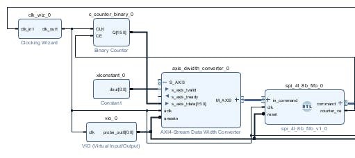
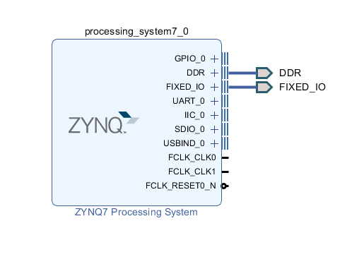
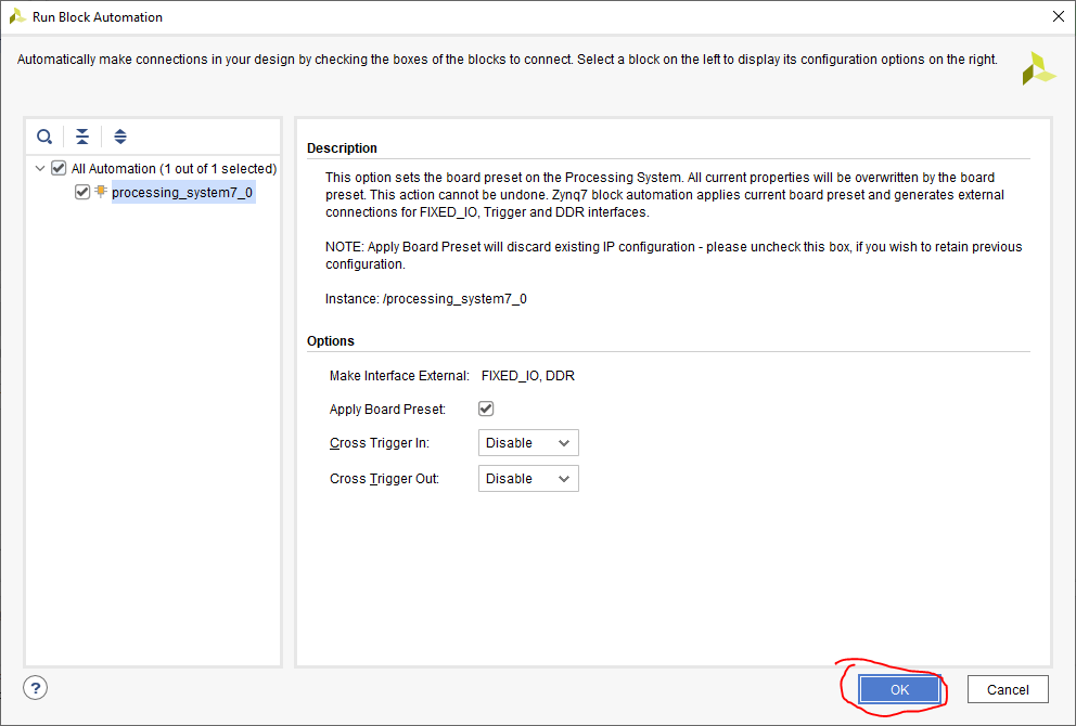
| {gallery}block design |
|---|
 |
|
|
 |
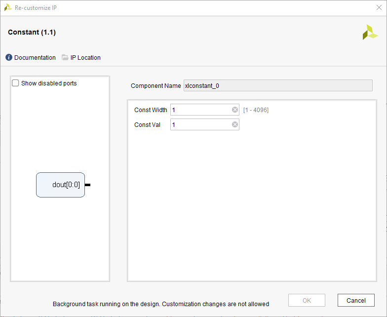
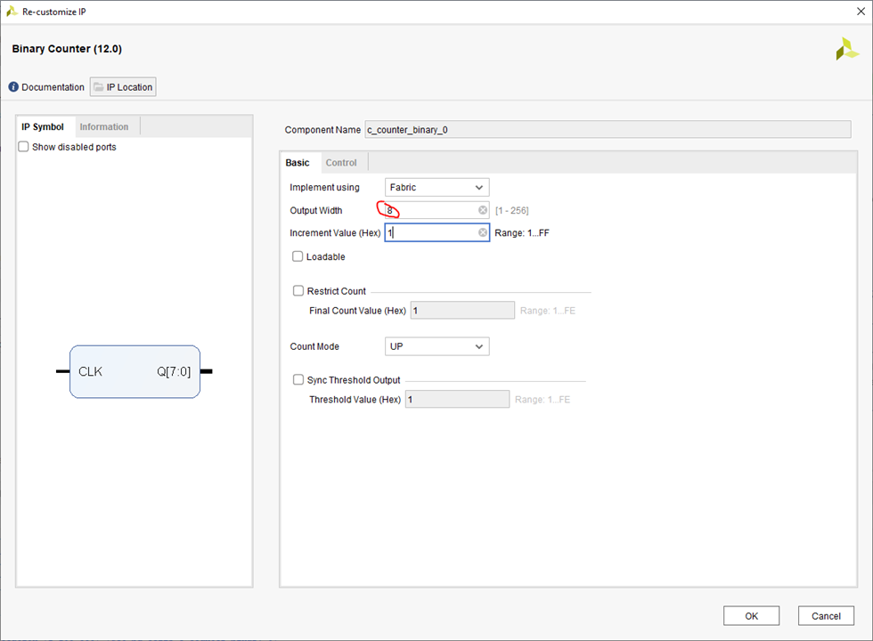
| {gallery}Block design Ips |
|---|
 |
 |
 |
 |
 |
|
|
 |
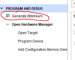
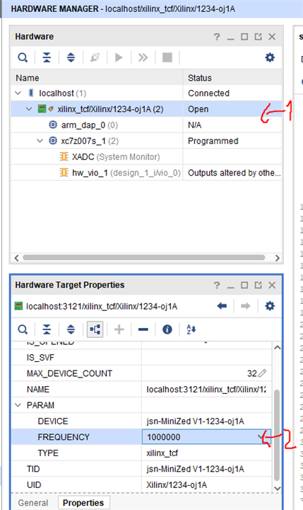
| {gallery}Program minized |
|---|
|
|
|
|
 |