


This blog will document my effort to make an SDR receiver using an Artix-7 FPGA reading multiple ADCs and sending the raw 16 bit samples over PCIe.
Problem of the moment:
Too many projects ... not enough time!
============================================================
A proof of concept has been built using a commercial SDR transceiver that had its FPGA lobotomized to do nothing but sample the ADC and send them over its Ethernet interface to a desktop PC
Once the samples have been processed into I/Q data with the Cuda board they can be used by various legacy SDR applications:

This concept is described in this youTube video:

I am using an AX7103 from Alinx as the prototype board for development:

At the moment I am learning the basics of Vivado. I have successfully modified a "blinky LED" demo and burned it to the board. The demos provided by Alinx assume use of windoz10 and Vivado 2019.1, so I have taken a side trip creating a Linux & Vivado 2022.2 version of the PDF that describes the basic project creation, synthesis, implementation, and programming cycles.
Links to sites describing FPGA/PCIe solutions:
Flyingbean kindly provided the following links to PCIe specific Xilinx code:
PCIE implementation on Artix 7
https://www.linkedin.com/pulse/xilinx-dma-pcie-tutorial-part-2-roy-messinger
The "official" Xilinx PCIe linux driver site:
After several requests Alinx sent me their driver that appears to originate with an old version of:
The Xilinx driver referred to in the current version of this answer is the one from the previous URL, while the included Alinx code appears to be from a company called SideBranch. Among other differences the Alinx code has a SideBranch copyright, while the official Xilinx driver iGPL2.
Books I'll be using:
- PCI Express Technology 3.0
- Linux Kernel Programming: A comprehensive guide to kernel internals, writing kernel modules, and kernel synchronization
- Linux Kernel Programming Part 2 - Char Device Drivers and Kernel Synchronization
- Mastering Linux Device Driver Development
- Linux Device Drivers, 3rd Edition
- Verilog by Example: A Concise Introduction for FPGA Design
- Advanced Digital Design With The Verilog Hdl, 2Nd Edn
- Verilog HDL A Guide to Digital Design and Synthesis
- Designing with Xilinx® FPGAs: Using Vivado
- FPGA to High speed ADC Data streaming, HDL programming: Xilinx Zynq7000 family on Vivado IDE platform
- Architecting High-Performance Embedded Systems
Well poo, my Vivado machine only has 8Gbyte, and that doesn't appear to be enough. Tried to build a DMA PCIe FPGA and it used all 8GByte + 2 GByte swap, and then dumps...
So I guess its time to find another build box 
Adventures installing & using Vivado and friends.
I decided to use 2019.1 as that is what Alinx uses and recommends. It installed cleanly on Ubuntu 22.10, but didn't work. Vivado uses Eclipse plugins with Java, and they are not at all happy with the most recent Java used on Ubuntu. After diddling around a bit I realized it was a lost cause and went on to install 2022.2.
I've moved the Vivado install specific info to here.
Some of the Alinx included IP is considered "out of date" by 2022.2. Guess I'll just have to slog thru that one issue at a time 
============================================================
December 17, 2022
Making some progress:

Working on the Alinx provided linux driver now, lots of deprecated functions, signature changes, etc. 
Too many Alinx drivers to fix, so I tried the current official Xilinx DMA driver from the Xilinx site. It only had 4 or 5 lines to fix.
$ cat /tmp/run_test.out
Info: Number of enabled h2c channels = 2
Info: Number of enabled c2h channels = 2
Info: The PCIe DMA core is memory mapped.
Info: Running PCIe DMA memory mapped write read test
    transfer size:  1024, count: 1
Info: Writing to h2c channel 0 at address offset 0.
Info: Writing to h2c channel 1 at address offset 1024.
Info: Wait for current transactions to complete.
/dev/xdma0_h2c_0 ** Average BW = 1024, 17.243992
/dev/xdma0_h2c_1 ** Average BW = 1024, 18.319736
Info: Writing to h2c channel 0 at address offset 2048.
Info: Writing to h2c channel 1 at address offset 3072.
Info: Wait for current transactions to complete.
/dev/xdma0_h2c_0 ** Average BW = 1024, 35.305473
/dev/xdma0_h2c_1 ** Average BW = 1024, 34.419010
Info: Reading from c2h channel 0 at  address offset 0.
Info: Reading from c2h channel 1 at  address offset 1024.
Info: Wait for current transactions to complete.
/dev/xdma0_c2h_0 ** Average BW = 1024, 14.353195
/dev/xdma0_c2h_1 ** Average BW = 1024, 32.647858
Info: Reading from c2h channel 0 at  address offset 2048.
Info: Reading from c2h channel 1 at  address offset 3072.
Info: Wait for current transactions to complete.
/dev/xdma0_c2h_0 ** Average BW = 1024, 16.967688
/dev/xdma0_c2h_1 ** Average BW = 1024, 18.439154
Info: Checking data integrity.
Info: Data check passed for address range  0 - 1024
Info: Data check passed for address range  1024 - 2048
Info: Data check passed for address range  2048 - 3072
Info: Data check passed for address range  3072 - 4096
Info: All PCIe DMA memory mapped tests passed.
Info: All tests in run_tests.sh passed.
I found that having the JTAG connected during boot causes the FPGA board to fail its boot cycle. If I remove it before rebooting the box it comes up properly. I then discovered that board hang on power-up doesn't occur when the JTAG is attached to the same box that the devel board is in. Probably something about how power comes up on the board and the JTAG.
============================================================
December 29, 2022
It took MANY tries to get the vendor's reference design working as I wanted. I've mastered that, thought it might have a wider audience so I created a stand-alone blog on the topic:
Making a Vivado Development Board Reference Design Your Own
============================================================
December 30, 2022
Found a very useful intro to beginner's FPGA programming.
I've learned to use the linux version of reg_rw (from the driver tools dir) to access the 4 status LEDS on the board. Wrote my own LED specific version, got that working.
The code provided by Alinx has a windoz specific program called xdma_rw which give access to all (most?) of the driver devices. I'm currently porting that to linux. Having trouble using memcpy() with the mmap'ed device memory. Think it is an issue with the 64 bit reads memcpy() uses and the ability of the device to satisfy them. for (x = 0; x < len; ++x) a=b; works...
The memcpy() error results in the driver not being able to see the device any longer, hopefully the lemonade here will be my figuring out a better way to recover than restarting linux.
============================================================
January 2023
I've ported a handful of tools from the windoz version of the driver package to linux:
- simple_dma.exe
- streaming_dma.exe
- user_event.exe
- xdma_info.exe
- xdma_rw.exe
- xdma_test.exe
xdma_info is particularly interesting:
$ sudo ./xdma_info
Found 1 XDMA devices
Device path:	/dev/xdma0_
Memory mapped at address 0x7fee63bb6000, length: 0x7000.


H2C Module
Channel ID:		0
 Version:		2017.1
 Streaming:		false
 Running:		false
 IE descr stop:		true
 IE descr complete:	true
 IE align mismatch:	true
 IE magic stopped:	true
 IE invalid length:	false
 IE idle stopped:	false
 IE read error:		1f
 IE write error:	0
 IE descr error:	1f
 Non incremental mode:	false
 Pollmode wb:		false
 AXI-ST wb disabled:	false
 Busy:			false
 Descriptor stopped:	false
 Descriptor completed:	false
 Alignment mismatch:	false
 Magic stopped:		false
 Invalid length:	false
 Idle stopped:		false
 Read error:		0x0
 Write error:		0x0
 Descriptor error:	0x0
 Completed Descriptors:	1
 Addr Alignment:	1 bytes
 Len Granularity:	1 bytes
 Addr bits:		64 bits
 Poll wb addr lo:	0x0
 Poll wb addr hi:	0x0
 IM Descr stopped:	true
 IM Descr completed:	true
 IM Alignment mismatch:	true
 IM Magic stopped:	true
 IM Invalid length:	false
 IM Idle stopped:	false
 IM Read error:		0x1f
 IM Write error:	0x0
 IM Descriptor error:	0x1f

Channel ID:		1
 Version:		2017.1
 Streaming:		false
 Running:		false
 IE descr stop:		true
 IE descr complete:	true
 IE align mismatch:	true
 IE magic stopped:	true
 IE invalid length:	false
 IE idle stopped:	false
 IE read error:		1f
 IE write error:	0
 IE descr error:	1f
 Non incremental mode:	false
 Pollmode wb:		false
 AXI-ST wb disabled:	false
 Busy:			false
 Descriptor stopped:	false
 Descriptor completed:	false
 Alignment mismatch:	false
 Magic stopped:		false
 Invalid length:	false
 Idle stopped:		false
 Read error:		0x0
 Write error:		0x0
 Descriptor error:	0x0
 Completed Descriptors:	1
 Addr Alignment:	1 bytes
 Len Granularity:	1 bytes
 Addr bits:		64 bits
 Poll wb addr lo:	0x0
 Poll wb addr hi:	0x0
 IM Descr stopped:	true
 IM Descr completed:	true
 IM Alignment mismatch:	true
 IM Magic stopped:	true
 IM Invalid length:	false
 IM Idle stopped:	false
 IM Read error:		0x1f
 IM Write error:	0x0
 IM Descriptor error:	0x1f


C2H Module
Channel ID:		0
 Version:		2017.1
 Streaming:		false
 Running:		false
 IE descr stop:		true
 IE descr complete:	true
 IE align mismatch:	true
 IE magic stopped:	true
 IE invalid length:	false
 IE idle stopped:	false
 IE read error:		1f
 IE write error:	0
 IE descr error:	1f
 Non incremental mode:	false
 Pollmode wb:		false
 AXI-ST wb disabled:	false
 Busy:			false
 Descriptor stopped:	false
 Descriptor completed:	false
 Alignment mismatch:	false
 Magic stopped:		false
 Invalid length:	false
 Idle stopped:		false
 Read error:		0x0
 Write error:		0x0
 Descriptor error:	0x0
 Completed Descriptors:	1
 Addr Alignment:	1 bytes
 Len Granularity:	1 bytes
 Addr bits:		64 bits
 Poll wb addr lo:	0x0
 Poll wb addr hi:	0x0
 IM Descr stopped:	true
 IM Descr completed:	true
 IM Alignment mismatch:	true
 IM Magic stopped:	true
 IM Invalid length:	false
 IM Idle stopped:	false
 IM Read error:		0x1f
 IM Write error:	0x0
 IM Descriptor error:	0x1f

Channel ID:		1
 Version:		2017.1
 Streaming:		false
 Running:		false
 IE descr stop:		true
 IE descr complete:	true
 IE align mismatch:	true
 IE magic stopped:	true
 IE invalid length:	false
 IE idle stopped:	false
 IE read error:		1f
 IE write error:	0
 IE descr error:	1f
 Non incremental mode:	false
 Pollmode wb:		false
 AXI-ST wb disabled:	false
 Busy:			false
 Descriptor stopped:	false
 Descriptor completed:	false
 Alignment mismatch:	false
 Magic stopped:		false
 Invalid length:	false
 Idle stopped:		false
 Read error:		0x0
 Write error:		0x0
 Descriptor error:	0x0
 Completed Descriptors:	1
 Addr Alignment:	1 bytes
 Len Granularity:	1 bytes
 Addr bits:		64 bits
 Poll wb addr lo:	0x0
 Poll wb addr hi:	0x0
 IM Descr stopped:	true
 IM Descr completed:	true
 IM Alignment mismatch:	true
 IM Magic stopped:	true
 IM Invalid length:	false
 IM Idle stopped:	false
 IM Read error:		0x1f
 IM Write error:	0x0
 IM Descriptor error:	0x1f


IRQ Module
 Version:		2017.1
 User IRQ en mask:	0x3
 Chan IRQ en mask:	0xf
 User IRQ:		0x0
 Chan IRQ:		0x0
 User IRQ pending:	0x0
 Chan IRQ pending:	0x0
 User IRQ Vector 0:	0
 User IRQ Vector 1:	0
 User IRQ Vector 2:	0
 User IRQ Vector 3:	0
 User IRQ Vector 4:	0
 User IRQ Vector 5:	0
 User IRQ Vector 6:	0
 User IRQ Vector 7:	0
 User IRQ Vector 8:	0
 User IRQ Vector 9:	0
 User IRQ Vector 10:	0
 User IRQ Vector 11:	0
 User IRQ Vector 12:	0
 User IRQ Vector 13:	0
 User IRQ Vector 14:	0
 User IRQ Vector 15:	0
 Chan IRQ Vector 0:	0
 Chan IRQ Vector 1:	0
 Chan IRQ Vector 2:	0
 Chan IRQ Vector 3:	0
 Chan IRQ Vector 4:	0
 Chan IRQ Vector 5:	0
 Chan IRQ Vector 6:	0
 Chan IRQ Vector 7:	0

Config Module
 Version:		2017.1
 PCIe bus:		0
 PCIe device:		0
 PCIe function:		0
 PCIE MPS:		256 bytes
 PCIE MRRS:		512 bytes
 System ID:		0x1234
 MSI support:		true
 MSI-X support:		false
 PCIE Data Width:	128 bits
 PCIE Control:		0x1
 User PRG MPS:		4096 bytes
 User EFF MPS:		4096 bytes
 User PRG MRRS:		4096 bytes
 User EFF MRRS:		4096 bytes
 Write Flush Timeout:	0x0

H2C SGDMA Module
Channel ID:		0
 Version:		2017.1
 Streaming:		false
 Descr addr lo:		0x1a9e0020
 Descr addr hi:		0x0
 Adj Descriptors:	0
 Descr credits:		0
Channel ID:		1
 Version:		2017.1
 Streaming:		false
 Descr addr lo:		0x1a820020
 Descr addr hi:		0x0
 Adj Descriptors:	0
 Descr credits:		0

C2H SGDMA Module
Channel ID:		0
 Version:		2017.1
 Streaming:		false
 Descr addr lo:		0x1a810020
 Descr addr hi:		0x0
 Adj Descriptors:	0
 Descr credits:		0
Channel ID:		1
 Version:		2017.1
 Streaming:		false
 Descr addr lo:		0x1a9b0020
 Descr addr hi:		0x0
 Adj Descriptors:	0
 Descr credits:		0

SGDMA Common Module
 Version:		2017.1
 Halt H2C descr fetch:	0x0
 Halt C2H descr fetch:	0x0
 H2C descr credit:	0x0
 C2H descr credit:	0x0
============================================================
February 1, 2023
I've made great progress. I now have a design with 2 FIFOs working:

I removed the smart connect, BRAM controller and BRAM memory generator, replacing them with the 2 FIFOs and changed the board from MM to Streaming.
I can write data into the FIFO thru the h2c ports, and read it back out thru the c2h ports. I plan to use the h2c path to stream dummy samples at the rate of 122.88Msps and then read them with a simple test jig designed to memmove() samples to the CUDA board FFT buffer. This way I can verify the critical path for timing, etc.
I have ADC sample files that I captured previously with the Anan200D transceiver. I believe I can stream them to the FIFO in the same manner and hear actual audio and decode digital modes.
Then it's just a matter (he says naively) of writing the ADC2AXI shim and rolling an ADC carrier...
===========================================================
February 13, 2023
Made some great progress! Built a tool to pace samples into the FIFO at the rate they would be clocked out of an ADC. Ran it over a day without issues:
reads: 3,081,000,002, chunks read: 3,081,000,000, bytes read: 12,619,776,000,000 in 28 hours, 31 minutes, 38 seconds (102698.972902522)
ideal: 3,080,940,000 chunks, difference: -60,000, 0.002%
Then I modified it to repeatedly send a chunk of actual samples I recorded a few years back during field day. That seemed to work. So I bit the bullet and wrote a program that emulates the way the Anan200D xcvr sends ADC samples to the SRD/Cuda program. I feed it a 512MB file, which is about 4.3 seconds of realtime data. Started it up and launched Athena:

She liked the samples. So I launched Aether:

Again, OK. Next I started a client, gqrx, a GNU Radio based receiver:

To my utter amazement there appears to be traffic!
I grabbed a soundbite, note that it repeats every 4 seconds, as that's the limit of the data I load into this test tool:
Gotta catch my breath, do some svn comits...
But I've proven this is all gonna work. Two issues to work on next:
- Write a verilog ADC2AXI shim to connect a real ADC to the front end of the FIFO.
- Roll a board to hold the ADC and connect it to the 2 40-pin connectors on the FPGA development board.
============================================================
February 16, 2023
I built a modular shelf system to hold prototype boards next to the PCIe/FPGA development card. It also supports the top edge of the card and gently presses it in to the slot connector:

Eventually I will be able to add another horizontal bar to hold the antenna bulkhead connectors. I have 40 pin IDC connectors and ribbon cable on the way from Amazon, as well as a small prototype board that has a 40 pin connector solder point. I'll add a row of pins for attaching oscilloscope probes and then see what I can tickle...
============================================================
February 24, 2023
I was able to run the pll experiment with output to a pin of the 40-pin connector ... pretty ratty looking clock...

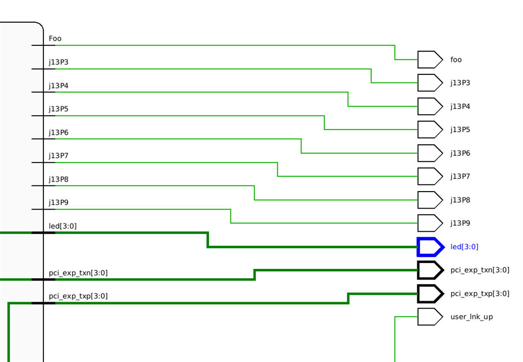
Went on to start defining the pins in my block design:
============================================================
February 26, 2023
ADC prototype board just arrived!!! FedEx actually delivered it on a Sunday, as it was scheduled for last Friday, but the
eastern snowstorms delayed it. Can't beat service like that.

============================================================
March 10, 2023
The ADC board needs a 50ohm clock, so after determining that signal generators in the 80MHz range are EXPENSIVE
I did some googling and found little boards based on the Si5351 chip. Thinking they were too good to be true more
googling showed that many hams are using them for xmitters and VFOs. So I bought one from Adafruit (they make
GREAT stuff).
Got it outputting both the 122.88MHZ that the 2208 needs, and 61.44MHz for the 2217:


Si provides a windoz tool to do all the necessary math for arbitrary frequencies:

Which outputs this:

Next step is to power up the ADC board with this clock attached ...
============================================================
March 14, 2023
I set up a jig to run the ADC board standalone:

The clock (aka. data valid) is on D15, sample bit A0 on D0, A4 on D4 and A8 on D8.
Running it with a 50ohm terminator shows a little noise:

Running it with an AlphaDelta Ultra antenna attached seems to see real data:

============================================================
March 28, 2023
It took several attempts to build an interface breadboard, my first mistake was too stupid to talk about...
The second try I used a board with traces running the length of the board:

It required cutting way too many traces, so try three. This board has no traces, only rows of 2-pin pads:

In the above pic I have notched out an area to clear the JTAG connector.
A connector for the PCIe card was placed on the bottom:

Then I added a connector for the ADC board, soldering it to the 1st connector:

With the ADC board added it looks like this:

Plenty of room for the Feather MCU and Si5351 oscillator. Next I will need to spend some time ringing everything out with an Ohm meter, looking for shorts, and verifying lines are attached properly.
============================================================
April 9, 2023
I've made some good progress. Everything on the breadboard rang out properly. I decided to temporarily convert the ADC lines into outputs to test the integrity of signal paths from FPGA pads to breadboard. Coded a verilog module to do this, as well as converting it into a Vivado module for placement on the Block Design Canvas. Both things I hadn't done before and thus quite useful in themselves!
The test shows all pins cycling properly:

I change them in blocks of 4 bits. The yellow trace is the Data Valid pin, I only have 16 digital inputs on my scope, so I had to use an analog probe for this bit. It correctly changes with the 4th block, eg. AD12 thru AD15.
At this point the design looks like:

The FPGA is getting a bit crowded, but I pretty much have everything I need. And I can remove the data generator and ADC0 test modules:
============================================================
April 10, 2023
The incoming ADC samples are 2 bytes wide, but the streaming FIFO is 16 bytes wide (PCIex4 * 32 bit transfer units). So I am using a streaming data-width converter to clock 8 samples, one at a time, into the converter, which clocks the 8 samples into the FIFO in one chunk
It occurred to me from yesterday's testing that I could write a module that would place pseudo samples into the data width converter to test that part of the puzzle.
It seems to work:
0x0000:  ffe0 ffe1 ffe2 ffe3 ffe4 ffe5 ffe6 ffe7 ffe8 ffe9 ffea ffeb ffec ffed ffee ffef
0x0010:  fff0 fff1 fff2 fff3 fff4 fff5 fff6 fff7 fff8 fff9 fffa fffb fffc fffd fffe ffff
0x0020:  0000 0001 0002 0003 0004 0005 0006 0007 0008 0009 000a 000b 000c 000d 000e 000f
0x0030:  0010 0011 0012 0013 0014 0015 0016 0017 0018 0019 001a 001b 001c 001d 001e 001f
The addresses on the left are arbitrary, ignore them. What is important is that they increment by one, without holes. They also properly roll over when reaching 0xffff.
Just for grins I sent the stream to the SDR, something is actually there:
So its time to actually plug the ADC board in and see what happens. But first I need to spend some time playing with it on the scope. Its powered by a 3.3v supply, so I mistakenly assumed it output 3.3v CMOS signals. But it appears to be putting out 2.5v CMOS... I *think* I know why.
============================================================
April 12, 2023
It works!!!
I apologize for the content, all I can see are strong local AM stations. But this clearly demonstrates a working system!
The "deafness" is caused by the front end on the demo board. It's designed for a 0-2.5v range. They expect it to be connected to signal generators, instruments, sensors, etc. The power on an antenna is typically measured in micro-volts. Thus all I can see are the really powerful locals. I was warned when I chose this board that it would be an issue.
So the final step for the R&D phase of this project is to design and build a proper RF front end with pre-amp to replace the one on the board.

============================================================
April 13, 2023
I redid the prototype shelf. Larger, using a 200mm PCIe card riser to bring the card out where I can access it:

Seems to work just fine.
============================================================
April 20, 2023
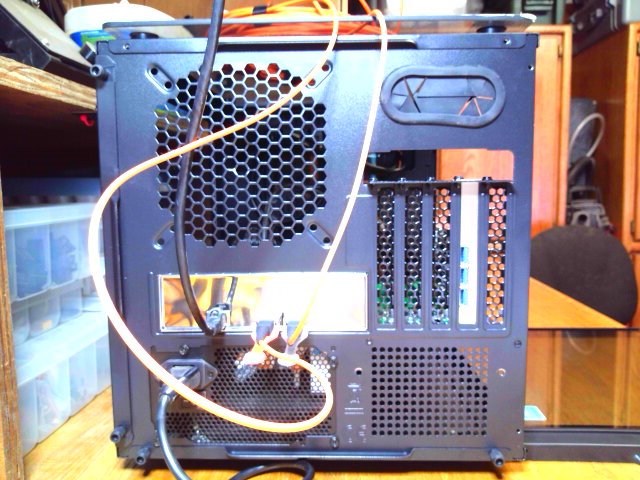
So I realized it was time to move the PCIe/FPGA card to the Radio box, ie the box with the Cuda processor & software. The original case was what is called an "inverted case". It holds the motherboard "upside down", making the PCIe cards face upwards. This box is a standard case, so the cards face downwards. Bought a 600mm PCIe riser cable to allow me to twist it 180 degrees and thus get the board facing upwards. Still works fine on this long riser (frankly I'm amazed). Re-arranging the shelf area to get working room, I realized I could route the cable out the backside of the cabinet. This allows the board to face upwards without twisting the cable, and locates it in a good position for a permanent case:

Started playing with the attenuator portion of the front end. Found that I get a MUCH lower noise floor with 21dB of attenuation.
Without any attenuation:

With 21dB attenuation:

Reception is MUCH better:
============================================================
April 26, 2023:
When I said "It works!!!" on April 12 I was a bit premature...
After getting a preamp on it and looking at the ham bands I realized the ONLY frequencies I could hear were the AM band. Even there frequencies were off by about 25KHz. Went crazy past week trying to figure it out. This was a good thing as I learned a lot about FPGA programming.
This is what AM looks like:

Compare to the image above from April 20, much better!
This is the 20 meter ham band:

40 meter ham band:

WWV @ 5MHz:

It appears to be 170 hz off, will think about that later...
The block design:

============================================================
April 27, 2023
Started board layout for real connector boards:


Three of them will cost a whoping $9.00.
============================================================
April 28, 2023
I think the first (J13) board is ready, gonna' eyeball it tomorrow before ordering. I was planning on making a single board that would work in either expansion port, but it got too messy. This is the top view of the J13 port connector. It will replace the breadboard that I am currently using:
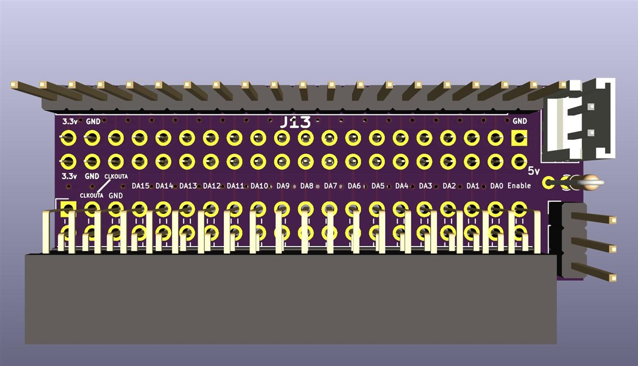
This is the bottom view:

============================================================
April 30, 2023
I decided to make it as one board for both ADCs:

Order placed with OshPark, should have them in 7-8 days.
The 854D boards are wider than the connectors, and would have hit one another, so I flipped the 2nd 180 degrees and placed below the board plane.
Digikey had one 854D-A (2208) available today, so I snatched it up! This is the part I wanted to use in the first place, but none were available anywhere...
---------------
Later in the day:
Two screen shots taken within a few moments of each other. The first is my anan200D:

This is the Phoenix (PCIe/FPGA card with 854D-E development board):

============================================================
May 1, 2023
I evidently have lost my mind, I just bought:
Support for 4 PCIe x4 boards at up to 1 kilometer away
I bought the version with 10m fiber. This will get the box anywhere in the house I want it for now. Eventually this would allow me to place the Phoenix receiver up in my observatory, which is on top of the highest part of the property, about 450' away. Perfect location for a receive-only antenna farm. I could support 4 x 2 ADCs. You can also attach 2 different motherboards via the 2 optical channels, which would allow 2 x 2 ADCs in 2 different locations. Interesting antenna diversity possibilities.
And they're still in business after 4 years, so that's a good sign...I bought their PCIe x1 board for the Minerva project, never got to us it for that, but testing with other random PCIe boards showed it to work well.
============================================================
May 2, 2023
Started serious work on reworking Athena/Aether to grok multiple ADCs. This is a view from the cuda profiler. We use a "scrape & save" fft, which occurs every 0.0128 seconds:

Each of the gold lines on the top row are sample xfers from cpu memory to cuda memory. The "open" space between passes is whats free for processing the 2nd ADC and any running DDCs. My record was 57 DDCs during a test.
The small purple section is the actual fft, fir, etc processing of a collection of those samples, here it is shown expanded:

============================================================
May 5, 2023
Making slow, but steady progress. Going from 1 ADC to N ADCs is a BIG jump. I now have the cuda code processing 2 ADCs, but still have to make the "per receiver" stage deal.
Here is a profile of the cuda code running:

Note that there are now 2 clusters of fft, fir, etc. ADC0 then ADC1.
Here is an expanded view of those 2 clusters:

============================================================
May 6, 2023
Got the fiber PCIe extension board yesterday. Set it up with a USB card in it. Hooked up SDR box's keyboard and mouse, worked great! Wont setup with PCIe/ADC card till I get the connector boards back from fab.


It has a web configuration interface which is pretty slick:
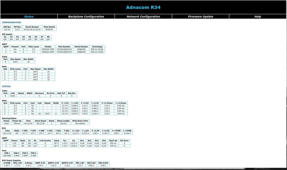
Note in the above status page it shows the USB card (that I used for keyboard/mouse test) plugged into slot 4. There is an ethernet port on the master fiber card which fits into the SDR desktop that should allow me to access the webpage without needing to run an ethernet cable to the ADC cube.
Figured out how to deal with the "which ADC has which virtual receiver" problem. Only create receivers with ADC 0 for now. All the cuda fft processing is done for all ADCs, but when the code gets to the cuda "per receiver" section I only proceed with ADC 0. This way I prove all ADCs are being processed, but don't cause the corruption by multiple ADCs attempting to create receivers.
I can choose which ADC will create receivers from the command line:
- --adc 0 pcie:0:0 --adc 1 iface:eno0
will use the PCIe/FPGA connected ADC for receivers while:
- --adc 0 iface:eno0 --adc 1 pcie:0:0
will use the anan200D connected via ethernet.
This will allow me to go forward with the hardware development without further Cuda programming till I figure out exactly what I want to accomplish...
============================================================
May 9. 2023
Well, today started out pretty bad....
Discovered that I forgot to refill the zones before sending in the gerbers, so no ground plane ( ground net) on new connector boards. Was able to patch them up, but pretty ugly:
 \
\
I expanded the FPGA pad test to cycle all 16 + 1 bits. Both J13 and J11 look good:

2nd ADC (J11) didn't work on first test. Found several errors in the FPGA code, fixed.
The 2217 works in both J13 and J11 - burned the .bin image, saved the project. Documented stuff. Time for some serious drinking!
============================================================
May 10, 2023
PCIe/FPGA card, both ADCs in cube - they work!

Now I gotta' shut it down and mount everything properly before I let the smoke out!
============================================================
May 12, 2023
Discovered that FPGA failed to run about 3 of every 4 powerups on fiber extender. Worked with customer support @ AdnaCom to fix. Literally 30-40 email exchanges, suggestions for improving my verilog design, etc. occurred. He sent me a modified .bin for the board, which solved the problem! I honestly have never experienced better customer support in my career.
Turns out that many FPGA designs do not meet strict PCIe timing specs because of the time it takes to load and configure the FPGA. Evidentially that is the case with my design. His fix was extending the PCIe bus reset from 100ms to one second. Doesn't sseem to do any harm, and FPGA configures properly every time (well, in about 20 tests so far)
============================================================
May 13, 2023
Have the ADCs properly mounted on a mezzanine board above the PCIe/FPGA board:

Expect BNC bulkhead connectors and LMR240 cable to arrive today. Then I can dress and route the antenna inputs properly an fit the top on the Cube.
Also have to mount the MCU properly, but that should be relatively easy.
============================================================
May 14, 2023
All done (with the case anyways ... at least for now):


============================================================
June 4, 2023
Replaced the 3.3v switcher with a Topping P50 ultra low noise linear PS. This supply has 2 5v 1.5A outputs, and 1 15v 1A output.
Measured draw on 1st 5v output is 0.8 amps for both ADCs. The 15v output powers a GALI-52+ MMIC preamp. Burned out 2 prototypes by getting clever and using an adjustable regulator to provide the 4.5v it wants, instead of using the 210ohm on 15v that the app sheet specifies. Evidently its doing much more than just dropping the voltage, but that's above my pay grade...

Started design of the PCB version:


============================================================
June 7, 2023
Finally received the updated adaptor boards:

Finished board looks much nicer when you remember to add the ground plane gerber!
Changed the ADC clock line to an FPGA clock qualified line (only one available per 40 pin connector). This eliminated a critical warning I had been ignoring since day one... Went from 2 layer to 4 layer: ground. ADC samples lines, ground, clock line.

============================================================
June 8, 2023
Sent the front-end PCB design to fab, already assigned to a panel:

Made a mock-up of a board and confirmed it will fit in the case I chose:

This will be my first attempt at an SMD board. Ordered a stainless steel stencil:

============================================================
June 9, 2023
Nothing to do hardware-wise till the new PCBs arrive. So I decided to install my new RTX4090 Cuda board:

The standard version of current RTX boards is about 3-1/2 slots wide, BIG fans! Got a liquid cooled version, which shrinks the slot width back to 2, but adds a large radiator. Built a frame to mount it on the side of the cabinet. Someday I'll get a piece of Lexan, cut a hole for the radiator and close the cabinet up.
Had been using a GTX980, which has 2048 cuda cores. This new RTX4090 has 16384 cores. But I was processing one ADC @ 61.44MSps. Hope to be processing 2 ADCs @ 122.88MSps. Which means about 4 times the data, so its not that big a jump...
============================================================
June 18, 2023:
Finished 1st 2 front ends:

Top is a 30MHz LPF (Low Pass Filter) with a GALI-52+ pre-amp.
Bare board will be built up with a GALI-74+ pre-amp.
Bottom module is a 30MHz LPF, but without any pre-amp.
When I'm satisfied with them will build a 2nd set for the 2nd ADC.
This pretty much brings me to the end of FPGA work (famous last words...). Looking for a ham/sw blog site to continue the discussion, Will post a link here if/when I do.


