element14 Community
element14 Community
    Register Log In
  • Site
  • Search
  • Log In Register
  • Community Hub
    Community Hub
    • What's New on element14
    • Feedback and Support
    • Benefits of Membership
    • Personal Blogs
    • Members Area
    • Achievement Levels
  • Learn
    Learn
    • Ask an Expert
    • eBooks
    • element14 presents
    • Learning Center
    • Tech Spotlight
    • STEM Academy
    • Webinars, Training and Events
    • Learning Groups
  • Technologies
    Technologies
    • 3D Printing
    • FPGA
    • Industrial Automation
    • Internet of Things
    • Power & Energy
    • Sensors
    • Technology Groups
  • Challenges & Projects
    Challenges & Projects
    • Design Challenges
    • element14 presents Projects
    • Project14
    • Arduino Projects
    • Raspberry Pi Projects
    • Project Groups
  • Products
    Products
    • Arduino
    • Avnet Boards Community
    • Dev Tools
    • Manufacturers
    • Multicomp Pro
    • Product Groups
    • Raspberry Pi
    • RoadTests & Reviews
  • Store
    Store
    • Visit Your Store
    • Choose another store...
      • Europe
      •  Austria (German)
      •  Belgium (Dutch, French)
      •  Bulgaria (Bulgarian)
      •  Czech Republic (Czech)
      •  Denmark (Danish)
      •  Estonia (Estonian)
      •  Finland (Finnish)
      •  France (French)
      •  Germany (German)
      •  Hungary (Hungarian)
      •  Ireland
      •  Israel
      •  Italy (Italian)
      •  Latvia (Latvian)
      •  
      •  Lithuania (Lithuanian)
      •  Netherlands (Dutch)
      •  Norway (Norwegian)
      •  Poland (Polish)
      •  Portugal (Portuguese)
      •  Romania (Romanian)
      •  Russia (Russian)
      •  Slovakia (Slovak)
      •  Slovenia (Slovenian)
      •  Spain (Spanish)
      •  Sweden (Swedish)
      •  Switzerland(German, French)
      •  Turkey (Turkish)
      •  United Kingdom
      • Asia Pacific
      •  Australia
      •  China
      •  Hong Kong
      •  India
      •  Korea (Korean)
      •  Malaysia
      •  New Zealand
      •  Philippines
      •  Singapore
      •  Taiwan
      •  Thailand (Thai)
      • Americas
      •  Brazil (Portuguese)
      •  Canada
      •  Mexico (Spanish)
      •  United States
      Can't find the country/region you're looking for? Visit our export site or find a local distributor.
  • Translate
  • Profile
  • Settings
FPGA
  • Technologies
  • More
FPGA
Blog FPGA Design Guide Pt4 - SPI Interface
  • Blog
  • Forum
  • Documents
  • Quiz
  • Events
  • Polls
  • Files
  • Members
  • Mentions
  • Sub-Groups
  • Tags
  • More
  • Cancel
  • New
Join FPGA to participate - click to join for free!
  • Share
  • More
  • Cancel
Group Actions
  • Group RSS
  • More
  • Cancel
Engagement
  • Author Author: pjclarke
  • Date Created: 17 Apr 2012 7:33 AM Date Created
  • Views 859 views
  • Likes 3 likes
  • Comments 3 comments
  • spi
  • fpga
  • vhdl
Related
Recommended

FPGA Design Guide Pt4 - SPI Interface

pjclarke
pjclarke
17 Apr 2012

So now that I have a working display I guess I had better get started on the SPI temperature sensor. The design process here is a little different as we are not just passing data or signals from one block to the next. What we need is a sub block that can process a few instruction to pull in the data from the SPI device.


image

image


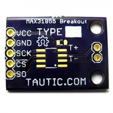
Now in some cases you may consider a state machine, but no. we first need to look at and think about what the SPI device delivers. The device I’ll be using is one I got from TAUTIChttp://store.tautic.com/ and uses a MAX31855http://datasheets.maxim-ic.com/en/ds/MAX31855.pdf. On page 5 we can the data pattern used that comes out of the device. It’s actually a very basic device to interface to. The chip select line goes low (CS) and then as the clock line is driven one bit of data comes out the device. There is a total of 32 bits (31 to 0) that need clocking out.


So the design can be done using a counter that counts out a number steps and during each step a different action takes place. We will need a few clock cycles to drive the CS line high, reseting the SPI device back to the start. Lets say we need 36 steps, that 32 for the data and a extra 4 for setting up and CS line etc. That’s more than enough.


So the code we write is going to need two sections, one that is a counter from 0 to 35 and another to drive the CS line and store data. It also needs to push the data out at the very end into a 32 bit wide signal what we can use. The counter is easy but what about the other sections?


Well we can start by just looking at the counter. When the counter has a value of 0 or 1 we can set the CS line high.  At count 2 we can drive the CS line low knowing that on the next clock we will get our first bit out. So thats count value 3 to 34 that will have valid data in them. These can be placed into a buffer that is shifted one bit every time too. hence data in collected one bit at a time. Once we get to count 34 we can ‘register’ the buffer into our 32 bit output. Registering it means its gets locked in so the buffer can be used again without effecting the output. It's actually nothing more that a big 32 bit latch. Also on count 34 and also during count 35 we will drive the CS line high and because our counter resets itself back to 0 when it sees 35, the whole thing starts all over again with no outside help. This is useful as we want a continuous flow of data from the temperature device.


Now this so far has all sounded quite a lot to do but as you will now see is not very much code at all.


entity SPI_Temp_Master is

    Port ( clk_i : in  STD_LOGIC;

            SPI_clk : out STD_LOGIC;

           SPI_cs : out  STD_LOGIC;

           SPI_Data_In : in  STD_LOGIC;

           SPI_Data_Out : out  STD_LOGIC_VECTOR (31 downto 0));

end SPI_Temp_Master;


Starting with the entity for this block we can see we have a incoming clock. We then have the interface to the SPI device which is a SPI_clk (clock output), SPI_cs (chip select) and SPI_Data_In which is the serial data from the device. Then we have the 32 bit output from the block which is called SPI_Data_Out.


signal SPI_rx_buff: std_logic_vector(31 downto 0);

signal SPI_cnt    : std_logic_vector(5 downto 0) := B"000000";

signal SPI_cs_sig : std_logic := '0';


The above signals will be used internally to the block as consist of the 32 bit buffer, our 6 bit counter (note its std_logic_vector) and then a chip select signal thats internal.


I then do a  bit of quick driving of the CS and clock line by having the following two lines.


SPI_cs <= SPI_cs_sig;

SPI_clk <= clk_i;


Next we need our counter noting that it resets when it sees a value of 35, back to 0. I have used the counter as a std_logic_vector as it fits with the rest of the design we have seen. Keeping consistent. People will be critical of me using the IEEE.STD_LOGIC_UNSIGNED.ALL library but for now this is about keeping it simple so I don't have to start explaining the whole which library debate. Just for now except that IEEE.STD_LOGIC_UNSIGNED.ALL is not great, but I’m using it anyway for now.


So our counter will look like this.


if SPI_cnt = 35 then

SPI_cnt <= (others => '0');

else

    SPI_cnt <= SPI_cnt + 1;

end if;


Notice that I’ve not included the process around this as yet, that because I’ll be wrapping the counter and the SPI block inside one process. This other block is as follows and should be easy to read.


if SPI_cnt < 2 then

    SPI_cs_sig <= '0';

    SPI_rx_buff <= (others => '0');

elsif SPI_cnt < 34 then

    SPI_rx_buff(31 downto 1) <= SPI_rx_buff(30 downto 0);

    SPI_rx_buff(0) <= SPI_Data_In;

    SPI_cs_sig <= '0';

elsif SPI_cnt = 34 then

    SPI_Data_Out(31 downto 0) <= SPI_rx_buff(31 downto 0);

    SPI_cs_sig <= '1';

else

    SPI_cs_sig <= '1';

end if;


So as you can see this block of code is lot shorter than my explanation.! The full file is included at the end of this post.


So we now have a working SPI unit that reads data out of our SPI device and pushes the result out once every 35 clock cycles, that’s quick. Our next stage is to plug this SPI block into our display logic we have done so far to get the final project working. That however will have to wait till next time.


Thanks

Paul (@monpjc)

Attachments:
SPI_Temp_Master.vhd.zip
  • Sign in to reply
  • cybero
    cybero over 7 years ago

    Hi Paul,

    I'm running your code I found something that looks like wrong.

    You're sampling during 34 clock cycles instead 32.


    See the attached picture: image

    • Cancel
    • Vote Up 0 Vote Down
    • Sign in to reply
    • More
    • Cancel
  • johnbeetem
    johnbeetem over 7 years ago in reply to cybero

    cybero  wrote:


    Hi Paul,

    Great job! I loved to find this entry in Google. Thanks for sharing your work.

    There's something confusing in your design.

    MAX31855 needs a 5MHz clock source. Your FPGA uses a 12MHz oscillator and I can't see a frequency divider in your design. SPI_clock comes from a 30 bit counter. Supposing clk_i comes from the 12MHz oscillator, that means SPI_clock is a 400KHz signal. Am I right?

    Looking at the MAX31855 data sheet, 5 MHz is the maximum serial clock frequency.  There is no minimum.   400 KHz should work fine.

    • Cancel
    • Vote Up 0 Vote Down
    • Sign in to reply
    • More
    • Cancel
  • cybero
    cybero over 7 years ago

    Hi Paul,

    Great job! I loved to find this entry in Google. Thanks for sharing your work.

    There's something confusing in your design.

    MAX31855 needs a 5MHz clock source. Your FPGA uses a 12MHz oscillator and I can't see a frequency divider in your design. SPI_clock comes from a 30 bit counter. Supposing clk_i comes from the 12MHz oscillator, that means SPI_clock is a 400KHz signal. Am I right?


    Can you please clarify how you get the 5MHz from your 12MHz oscillator?


    Thanks again.

    Cheers.

    • Cancel
    • Vote Up 0 Vote Down
    • Sign in to reply
    • More
    • Cancel
element14 Community

element14 is the first online community specifically for engineers. Connect with your peers and get expert answers to your questions.

  • Members
  • Learn
  • Technologies
  • Challenges & Projects
  • Products
  • Store
  • About Us
  • Feedback & Support
  • FAQs
  • Terms of Use
  • Privacy Policy
  • Legal and Copyright Notices
  • Sitemap
  • Cookies

An Avnet Company © 2025 Premier Farnell Limited. All Rights Reserved.

Premier Farnell Ltd, registered in England and Wales (no 00876412), registered office: Farnell House, Forge Lane, Leeds LS12 2NE.

ICP 备案号 10220084.

Follow element14

  • X
  • Facebook
  • linkedin
  • YouTube