


Field-programmable gate arrays (FPGAs) are reprogrammable silicon chips. They can be programmed for different algorithms after fabrication. Modern FPGAs consist of up to millions of logic cells that can be configured to implement a variety of software algorithms. Although the traditional FPGA design flow is more similar to a regular IC than a processor, an FPGA provides significant cost advantages in comparison to an IC development effort and offers the same level of performance in most cases.
Structure
The basic structure of an FPGA is composed of the following elements:
- Look-up table (LUT): This element performs logic operations.
- Flip-Flop (FF): This register element stores the result of the LUT.
- Wires: These elements connect elements to one another.
- Input/Output (I/O) Blocks: These ports get data in and out of the FPGA. Basically includes general-purpose input/output (GPIO) pins and pads
The LUT is the basic building block of an FPGA and is capable of implementing any logic function of N Boolean variables. Essentially, this element is a truth table in which different combinations of the inputs implement different functions to yield output values. The limit on the size of the truth table is N, where N represents the number of inputs to the LUT. For the general N-input LUT, the number of memory locations accessed by the table is 2N. This allows the table to implement 2N^N functions. In general, each CLB (Configurable Logic Block) is having 2 or 4 slices. Each slice is having 2 Logic Cell (LC)s and each logic cell has LUT as basic building blocks.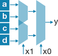
FPGAs are heterogeneous compute platforms that include Block RAMs, DSP Slices, PCI Express support, and programmable fabric. They enable parallelism and pipelining of applications across the entire platform as all of these compute resources can be used simultaneously. Contemporary FPGA architectures incorporate the basic elements along with additional computational and data storage blocks that increase the computational density and efficiency of the device. These additional elements, include: Embedded memories for distributed data storage, Phase-locked loops (PLLs) for driving the FPGA fabric at different clock rates, High-speed serial transceivers, Off-chip memory controllers, and Multiply-accumulate blocks (MAC). 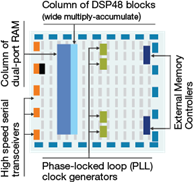 The DSP48 block is an arithmetic logic unit (ALU) embedded into the fabric of the FPGA and is composed of a chain of three different blocks. The computational chain in the DSP48 contains an add/subtract unit connected to a multiplier connected to a final add/subtract/accumulate engine.
Configuration Cell Technologies
The configuration bitstream can be stored inside FPGA using various technologies like SRAM-based, SRAM with internal flash memory, Flash based FPGAs, and Antifuse based FPGAs.
SRAM-based FPGAs: An SRAM-based FPGA stores logic cells’ configuration data in the static memory. Since SRAM is volatile and can't keep data without power source, such FPGAs must be programmed (configured) upon start. There are two basic modes of programming: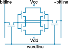
- Master mode, when FPGA reads configuration data from an external source, such as an external Flash memory chip.
- Slave mode, when FPGA is configured by an external master device, such as a processor. This can be usually done via a dedicated configuration interface or via a boundary-scan (JTAG) interface.
SRAM-based FPGAs with an internal flash memory: This type of FPGA is generally like the previous, except that these chips contain internal flash memory blocks, thus eliminating the need to have an external non-volatile memory. One example of such FPGAs is the Xilinx Spartan-3AN family. Each model of Spartan-3AN has an in-chip flash memory module with an SPI interface capable of storing two or more configuration bitstreams. The bitstream can be chosen during startup. Another example of such technology is the LatticeXP family by Lattice semiconductors. Using internal non-volatile memory can be also useful to prevent unauthorized bitstream copying.
Flash-based FPGAs: The true flash-based FPGAs shouldn't be confused with the previous type. The SRAM-based FPGAs with internal flash memory use flash only during startup to load data to the SRAM configuration cells. On the contrary, true flash-based FPGA uses flash as a primary resource for configuration storage, and doesn't require SRAM (a similar technology is used in CPLDs – complex programmable logic devices, but the FPGA architecture is very different from that of CPLD). This technology has an advantage of being less power consumptive. Flash-based FPGAs are also more tolerant to radiation effects. Flash-based FPGA families such as Igloo and ProASIC3 are manufactured by MicroSemi. As in the previous case, using flash-based FPGAs can be a solution to prevent unauthorized bitstream copying.
Antifuse-based FPGAs: Antifuse-based FPGAs are different from the previous ones in that they can be programmed only once. The antifuse is a device that doesn't conduct current initially, but can be “burned” to conduct current (the antifuse behavior is thus opposite to that of the fuse, hence the name). The antifuse-based FPGA can't be then reprogrammed since there is no way to return a burned antifuse into the initial state. Antifuse-based device families include Axcelerator produced by Microsemi.
| SRAM | Flash | Antifuse |
Actual Speed | Fast | Slow | Fast |
Density | Larger Structures Less dense | In Between | Smaller structures More Dense |
Voltatility | Volatile | Non-volatile | Non-volatile |
Reprogrammability | Yes | Yes | No |
Security | Low (bitstream accessible) | High (bitstream not accessible) | High (bitstream not accessible) |
Power Consumption | High | Low | Low |
Table 1: Comparison of SRAM, Flash and Antifuse FPGAs
FPGA Configuration
FPGA Configuration is the process of loading the FPGA chip with Configuration data through external devices during power “On” state. The method of configuring an FPGA can be divided into the following: Master Mode, Slave Mode and JTAG Mode.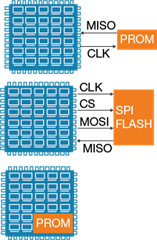
Master Mode: In the Master Mode the Configuration data is stored in external nonvolatile memories such as SPI FLASH, Parallel FLASH, PROM and so on. During the configuration process, the data is loaded in the FPGA Configurable Logic Blocks to operate as a specific application. The configuration clock is provided by FPGA in Master Mode operation.
Slave Mode: In Slave Mode, the entire configuration Process is controlled by an external device. Those external devices may be a processor, microcontroller, and so on. The Configuration can be performed by the serial or parallel method. The Clock input is supplied by the external device for Slave mode.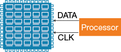
JTAG Mode: The four-wire JTAG interface is common on board testers and debugging hardware. FPGA mainly uses JTAG interface for prototype download and debugging. JTAG c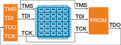 onsists of TCK, TMS, TDI and TDO lines for communication.
