This document is based on “Migrating Spartan-6 Designs to 7 Series & Beyond” document of Adam Taylor. There are a lot of interesting features in the new family and development tools. To describe these differences, I will use two cookies: A spartan 6-based board called Amiba 2 rev D, and a Spartan 7-based board identified as ARTY S7 in its version 50.

On one hand, Amiba 2 has an XC6SLX9 device. This one has 9152 Logic Cells, 16 DSP48A1, 32 Block RAMs, and 200 I/Os. On the other hand, Arty board has an XC7S50 device with a more nutrient efficiency. With 52160 logic cells, 120 DSP48E1, 75 Block RAMs, and 250 I/Os, this device has a lot of hours in a GYM. The Family overview shows constrained limits on each generation. Despite Spartan 6 reaches devices up to 147443 Logic cells compared with the maximum 102400 in 7 series, the technological step allows better use of the resources. One of the differences is that Slice_X type cells available in Spartan 6 will be mapped on Slices_L type cells.

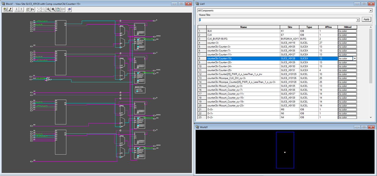
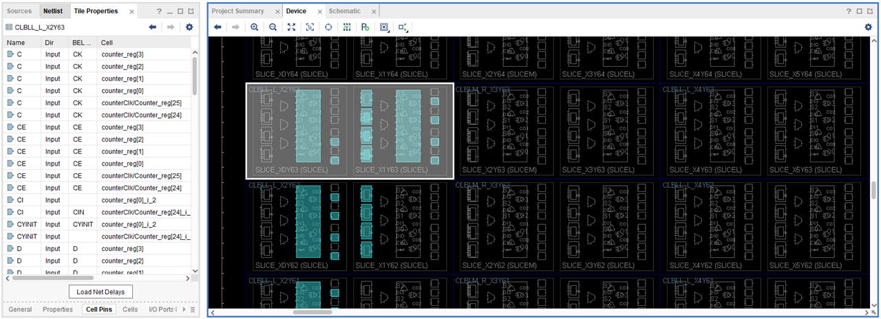
The figure above shows a digital circuit implemented on the Amiba 2 board. Here, is possible to observe the mapping on Slice_X and Slice_L cells. the image below represents the counterpart tool for the Arty board. Remember that Spartan 6 has a distributed toolbox while the Spartan 7 brings a new IDE where development, simulation, power analysis and more are centralized and organized in the same window. In the same figure is possible to observe the Slice_X absence.

While Amiba 2 uses 69 LUTs, the Arty requires 16 LUTs (Data is taken from the reports generated in each development platform). This shows a great improvement. For the nature of the test design, the synthesis requires the same number of Flip Flops and I/O ports. What is the test design? A 4-bit counter with Up/Down, Blocking, Load, and Reset control. A cross HDL approach was used to develop the counter and a clock divider. Remember the clock has a huge velocity to be perceived by the human eye, consequently, a divider is required to view the counter advance each second. The codes are below:
module CNT_4b(
	input CLK, UP, BLK, LOAD, RST, [3:0] D,
	output [3:0] Q
);

	wire divClk;
	integer counter;
	DIV counterClk(CLK, divClk);

	always@(posedge(divClk) or posedge(RST))
	begin
		if(RST) begin
			counter = 15;
		end else if(divClk) begin
			if(LOAD) begin
				counter = D;
			end else if(!BLK) begin
				if (UP) begin
					counter = counter + 1;
				end else begin
					counter = counter - 1;
				end
			end
		end
	end

	assign Q = counter;

endmodule
entity DIV is
    Port ( CLK : in  STD_LOGIC;
           CLK_DIV : out  STD_LOGIC);
end DIV;

architecture Behavioral of DIV is
	signal Counter: integer range 0 to 49_999_999 := 0;
begin

	process(CLK)
	begin
		if rising_edge(CLK) then
			if (Counter < 49_999_999) then
				Counter <= Counter + 1;
			else
				Counter <= 0;
			end if;
		end if;
	end process;

	process(Counter)
	begin
		if(Counter <= 25_000_000) then
			CLK_DIV <= '1';
		else
			CLK_DIV <= '0';
		end if;
	end process;

end Behavioral;
This is a dummy project to view some differences between the new 7 series and the 6 series. The migration for this design is very easy and quick, file import is required to achieve it. Only a file is required to be created in the new development, an XDC with all the I/O definitions as follows:
## Clock Signals
set_property -dict { PACKAGE_PIN F14   IOSTANDARD LVCMOS33 } [get_ports { CLK }]; #IO_L13P_T2_MRCC_15 Sch=uclk

## Switches
set_property -dict { PACKAGE_PIN H14   IOSTANDARD LVCMOS33 } [get_ports { D[0] }]; #IO_L20N_T3_A19_15 Sch=sw[0]
set_property -dict { PACKAGE_PIN H18   IOSTANDARD LVCMOS33 } [get_ports { D[1] }]; #IO_L21P_T3_DQS_15 Sch=sw[1]
set_property -dict { PACKAGE_PIN G18   IOSTANDARD LVCMOS33 } [get_ports { D[2] }]; #IO_L21N_T3_DQS_A18_15 Sch=sw[2]
set_property -dict { PACKAGE_PIN M5    IOSTANDARD SSTL135 } [get_ports { D[3] }]; #IO_L6N_T0_VREF_34 Sch=sw[3]

## LEDs
set_property -dict { PACKAGE_PIN E18   IOSTANDARD LVCMOS33 } [get_ports { Q[0] }]; #IO_L16N_T2_A27_15 Sch=led[2]
set_property -dict { PACKAGE_PIN F13   IOSTANDARD LVCMOS33 } [get_ports { Q[1] }]; #IO_L17P_T2_A26_15 Sch=led[3]
set_property -dict { PACKAGE_PIN E13   IOSTANDARD LVCMOS33 } [get_ports { Q[2] }]; #IO_L17N_T2_A25_15 Sch=led[4]
set_property -dict { PACKAGE_PIN H15   IOSTANDARD LVCMOS33 } [get_ports { Q[3] }]; #IO_L18P_T2_A24_15 Sch=led[5]

## Buttons
set_property -dict { PACKAGE_PIN G15   IOSTANDARD LVCMOS33 } [get_ports { RST }]; #IO_L18N_T2_A23_15 Sch=btn[0]
set_property -dict { PACKAGE_PIN K16   IOSTANDARD LVCMOS33 } [get_ports { LOAD }]; #IO_L19P_T3_A22_15 Sch=btn[1]
set_property -dict { PACKAGE_PIN J16   IOSTANDARD LVCMOS33 } [get_ports { BLK }]; #IO_L19N_T3_A21_VREF_15 Sch=btn[2]
set_property -dict { PACKAGE_PIN H13   IOSTANDARD LVCMOS33 } [get_ports { UP }]; #IO_L20P_T3_A20_15 Sch=btn[3]
In the new development boards from Xilinx or Digilent, there is available a bundle of files with all definitions from the respective web pages. This reduces the risk of user bad definitions. In the ISE Webpack we have a UCF file like this one:
NET "D[3]" IOSTANDARD = LVCMOS33;
NET "D[2]" IOSTANDARD = LVCMOS33;
NET "D[1]" IOSTANDARD = LVCMOS33;
NET "D[0]" IOSTANDARD = LVCMOS33;
NET "Q[3]" IOSTANDARD = LVCMOS33;
NET "Q[2]" IOSTANDARD = LVCMOS33;
NET "Q[1]" IOSTANDARD = LVCMOS33;
NET "Q[0]" IOSTANDARD = LVCMOS33;
NET "BLK" IOSTANDARD = LVCMOS33;
NET "CLK" IOSTANDARD = LVCMOS33;
NET "LOAD" IOSTANDARD = LVCMOS33;
NET "RST" IOSTANDARD = LVCMOS33;
NET "UP" IOSTANDARD = LVCMOS33;


NET "D[3]" LOC = P9;
NET "D[2]" LOC = N4;
NET "CLK" LOC = E7;
NET "LOAD" LOC = J4;
NET "RST" LOC = H4;
NET "UP" LOC = L1;
NET "BLK" LOC = K1;

# PlanAhead Generated physical constraints

NET "Q[0]" LOC = N9;
NET "Q[1]" LOC = M5;
NET "Q[2]" LOC = M3;
NET "Q[3]" LOC = R10;
NET "D[0]" LOC = M8;
NET "D[1]" LOC = N6;
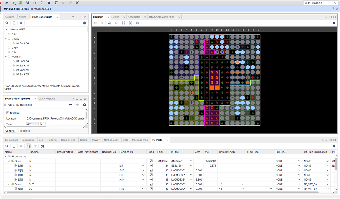
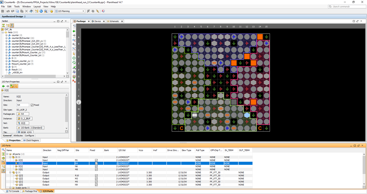
Amiba 2 has not this file directly, we need to view the datasheet or the text in the board to map the pins with the PlanAhead tool. To do the same process in Vivado, the I/O Planning tool could be used. Below on the up, the Vivado I/O Planning tool is presented, on the bottom, the PlanAhead tool is shown.


Here, I finish this first step in this FPGAs exploration. I will develop new projects and concepts to evolve in the development tools use.
