In my last blog on FPGAs, as a part of the 7 ways to Leave your Spartan-6 contest, I published an introductory blog on getting started with FPGAs and VHDL.
In the 2nd blog, I will discuss digital logic design using FPGAs. Here, I will cover the following design implementations -
1. How to design simple logic gates in VHDL and implement them on the FPGA
2. How to design advanced digital logic designs/architectures on FPGA
3. An example project to design and implement a random number generator on FPGA
Logic Gate Design
Let's start with the first design. I will implement simple logic gates on the FPGA, such as AND, OR, NOT, NOT, XOR, etc., on the FPGA. I will also demonstrate that the code written for these logic gates implements these gates inside the FPGA by checking the RTL schematic and running simulations.
First, let's start with a NOT gate. A NOT gate has one input and one output with the truth table as
| X (input) | Y(output) |
| 0 | 1 |
| 1 | 0 |
For this, I'll create a new project in vivado
Notice that I'm using VHDL here so my target language is set as VHDL
Next step is to write the VHDL code for a NOT gate. For this we have to add a source file. A source file is the one that contains the HDL code for our designs.
After this step we have to assign the ports. Now you may understand why we need to have the digital logic circuit designed in mind before writing VHDL code, because we should know the number of inputs and outputs. We can also change this later by typing the code, but I prefer assigning it in the module.
Here, I have assigned X as input and Y as output port.
Now, this will automatically generate the entity named "gate1" and architecture named "behavioral".
Note that this name has got nothing to do with behavioal type of coding in VHDL. In VHDL one can describe the architecture of the digital logic in three types - Behavioral, dataflow and structural. Here the name behavioral has got nothing to with the behavioral type of modelling in VHDL.
Upon clicking ok, this will automatically generate a simple code with entity and architecture blocks of code in the source file as shown here
Here you can see that the entity is named as gate1 with X as input and Y as output and an architecture block is also written where we have to write our logic for NOT gate.
The entire code for the NOT gate is shown below
----------------------------------------------------------------------------------
-- Company:
-- Engineer:
--
-- Create Date: 28.07.2022 22:57:31
-- Design Name:
-- Module Name: gate1 - Behavioral
-- Project Name:
-- Target Devices:
-- Tool Versions:
-- Description:
--
-- Dependencies:
--
-- Revision:
-- Revision 0.01 - File Created
-- Additional Comments:
--
----------------------------------------------------------------------------------


library IEEE;
use IEEE.STD_LOGIC_1164.ALL;

-- Uncomment the following library declaration if using
-- arithmetic functions with Signed or Unsigned values
--use IEEE.NUMERIC_STD.ALL;

-- Uncomment the following library declaration if instantiating
-- any Xilinx leaf cells in this code.
--library UNISIM;
--use UNISIM.VComponents.all;

entity gate1 is
    Port ( X : in STD_LOGIC;
           Y : out STD_LOGIC);
end gate1;

architecture Behavioral of gate1 is

begin
Y <= not(X);

end Behavioral;
Next, click on run-> run synthesis
Once synthesis is complete, run implementation.
Now let's check how the design that we wrote the code for actually looks like, under RTL analysis click on schematic
This is how the RTL schmatic for our code looks like. It is a simple NOT gate with X as input and Y as output.
Similarly, the codes for AND gate and OR gate are as shown below
----------------------------------------------------------------------------------
-- Company:
-- Engineer:
--
-- Create Date: 28.07.2022 22:57:31
-- Design Name:
-- Module Name: gate1 - Behavioral
-- Project Name:
-- Target Devices:
-- Tool Versions:
-- Description:
--
-- Dependencies:
--
-- Revision:
-- Revision 0.01 - File Created
-- Additional Comments:
--
----------------------------------------------------------------------------------


library IEEE;
use IEEE.STD_LOGIC_1164.ALL;

-- Uncomment the following library declaration if using
-- arithmetic functions with Signed or Unsigned values
--use IEEE.NUMERIC_STD.ALL;

-- Uncomment the following library declaration if instantiating
-- any Xilinx leaf cells in this code.
--library UNISIM;
--use UNISIM.VComponents.all;

entity gate1 is
    Port ( X : in STD_LOGIC;
           Y : in STD_LOGIC;
           Z : out STD_LOGIC);
end gate1;

architecture Behavioral of gate1 is

begin
Z <= X AND Y;

end Behavioral;
----------------------------------------------------------------------------------
-- Company:
-- Engineer:
--
-- Create Date: 28.07.2022 22:57:31
-- Design Name:
-- Module Name: gate1 - Behavioral
-- Project Name:
-- Target Devices:
-- Tool Versions:
-- Description:
--
-- Dependencies:
--
-- Revision:
-- Revision 0.01 - File Created
-- Additional Comments:
--
----------------------------------------------------------------------------------


library IEEE;
use IEEE.STD_LOGIC_1164.ALL;

-- Uncomment the following library declaration if using
-- arithmetic functions with Signed or Unsigned values
--use IEEE.NUMERIC_STD.ALL;

-- Uncomment the following library declaration if instantiating
-- any Xilinx leaf cells in this code.
--library UNISIM;
--use UNISIM.VComponents.all;

entity gate1 is
    Port ( X : in STD_LOGIC;
           Y : in STD_LOGIC;
           Z : out STD_LOGIC);
end gate1;

architecture Behavioral of gate1 is

begin
Z <= X OR Y;

end Behavioral;
From the simulation results once can verify if our code is correct or not.
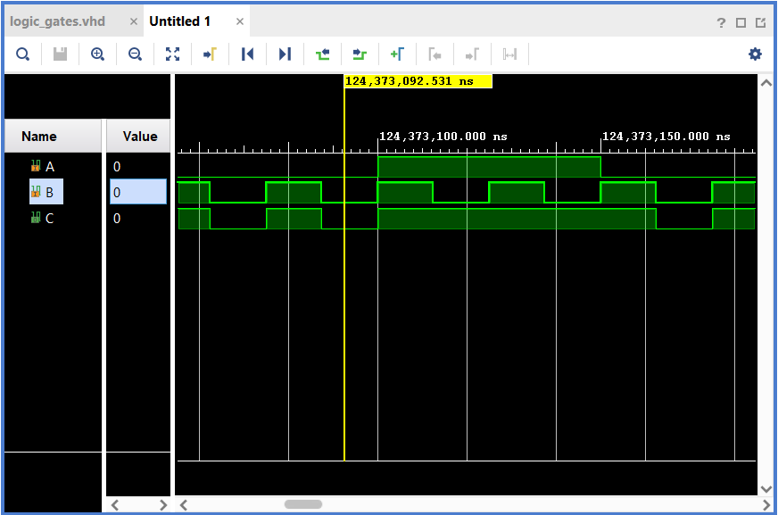
Here, we can see that for A=0,B=0, C=0, and A=0, B=1 C =1, which shows that this is OR logic.
Let's look at some advanced designs now.
Multiplexer Design
I want to design a 4:1 MUX (multiplexer) in VHDL and implement it on the FPGA. For this first, let's look at the MUX as a block. A 4:1 MUX will have 4 (data lines) + 2(select lines) = 6 inputs and 1 output.
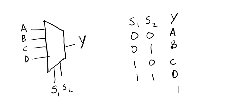
Here's the code for the 4:1 MUX
----------------------------------------------------------------------------------
-- Company:
-- Engineer:
--
-- Create Date: 04.08.2022 23:04:51
-- Design Name:
-- Module Name: mux - Behavioral
-- Project Name:
-- Target Devices:
-- Tool Versions:
-- Description:
--
-- Dependencies:
--
-- Revision:
-- Revision 0.01 - File Created
-- Additional Comments:
--
----------------------------------------------------------------------------------


library IEEE;
use IEEE.STD_LOGIC_1164.ALL;

-- Uncomment the following library declaration if using
-- arithmetic functions with Signed or Unsigned values
--use IEEE.NUMERIC_STD.ALL;

-- Uncomment the following library declaration if instantiating
-- any Xilinx leaf cells in this code.
--library UNISIM;
--use UNISIM.VComponents.all;

entity mux is
    Port ( A : in std_logic_vector(3 downto 0);
           S : in std_logic_vector(1 downto 0);
           Y : out std_logic);
end mux;

architecture Behavioral of mux is

begin
process (S,A)

begin


if (S <= "00") then
Y <= A(0);
elsif (S <= "01") then
Y <= A(1);
elsif (S <= "10") then
Y <= A(2);
else
Y <= A(3);

end if;
end process;

end Behavioral;
Here, a vector can be considered a bus in VHDL it is defined as a vector. 3 downto 0 means A(3), A(2), A(1) and A(0) -> 4 inputs. Similarly for the select lines, S is defined as a vector with size 2.
The simplified schematic is shown below
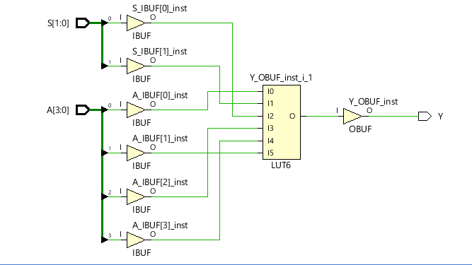
Moving to a more advanced level, I will design an LFSR-based random number generator.
LFSR based Random Number Generator
Random numbers are used in many applications such as online games, 2-factor authentication, one-time password, cryptography, etc. There are various ways to generate random numbers. Usually, the numbers generated using digital algorithms are pseudo-random in nature as they are deterministic and repeat after certain states. LFSR stands for Linear Feedback Shift register, a technique used to generate random numbers. LFSR employs shift registers and XOR gates to generate random numbers.
To test the random number generator, I will use a test bench. A test bench is essentially a separate code written to evaluate or test the performance of our main logic/original VHDL code. A test bench will contain various statements that will be run through the initial VHDL code and tested for any errors and correct outputs.
A test bench code has to be defined under simulation sources in Vivado.

--Code for LFSR Random Number Generator

library IEEE;
use IEEE.STD_LOGIC_1164.ALL;
entity pseudorng is
Port ( clock : in STD_LOGIC;
reset : in STD_LOGIC;
en : in STD_LOGIC;
Q : out STD_LOGIC_VECTOR (7 downto 0);
check: out STD_LOGIC);
end pseudorng;
architecture Behavioral of pseudorng is
signal Qt: STD_LOGIC_VECTOR(7 downto 0) := x"01";
begin
PROCESS(clock)
variable tmp : STD_LOGIC := '0';
BEGIN
IF rising_edge(clock) THEN
IF (reset='1') THEN
Qt <= x"01"; --for 0 it will enter redundant state of all 0's
ELSIF en = '1' THEN
tmp := Qt(4) XOR Qt(3) XOR Qt(2) XOR Qt(0);
Qt <= tmp& Qt(7 downto 1);
END IF;
END IF;
END PROCESS;
-- check <= temp;
check <= Qt(7);
Q <= Qt;
end Behavioral;
Test bench code-
library IEEE;
use IEEE.STD_LOGIC_1164.ALL;

entity tb_pseudorng is
end tb_pseudorng;

architecture bench of tb_pseudorng is

COMPONENT pseudorng
      Port ( clock : in STD_LOGIC;
      reset : in STD_LOGIC;
      en : in STD_LOGIC;
      Q : out STD_LOGIC_VECTOR (7 downto 0);
      check: out STD_LOGIC);
END COMPONENT;

signal clock1: STD_LOGIC;
signal reset1: STD_LOGIC;
signal Q1: STD_LOGIC_VECTOR(7 downto 0);
signal check1: STD_LOGIC;
signal en : STD_LOGIC;

begin

mapping: pseudorng PORT MAP(
clock => clock1,
reset => reset1,
en => en,
Q => Q1,
check => check1);

clock: PROCESS
BEGIN
   clock1 <= '0'; wait for 50 ns;
   clock1 <= '1'; wait for 50 ns;
END PROCESS;

reset: PROCESS
BEGIN
   reset1 <= '0';
   en <= '1';
   wait for 900 ns;
END PROCESS;

end bench;
Here's what the RTL logic for LFSR looks like. As I said, it is a linear feedback shift register means that there will be shift registers with feedback (a connection from output to input).
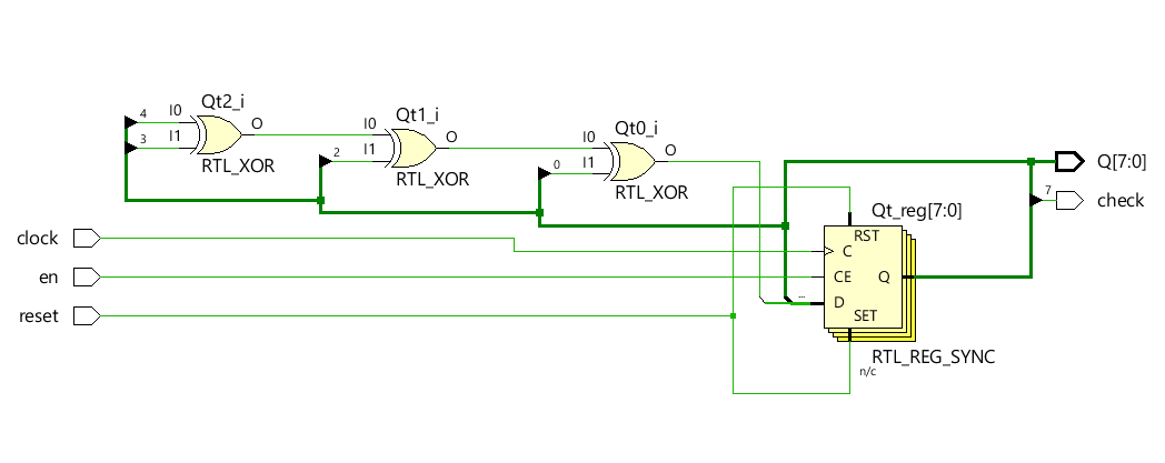
It has three inputs, clock, enable and reset. And since this uses four shift registers, it can generate 255 distinct random numbers.
As seen from the simulation results, at each clock pulse, a new number is generated at the output Q1
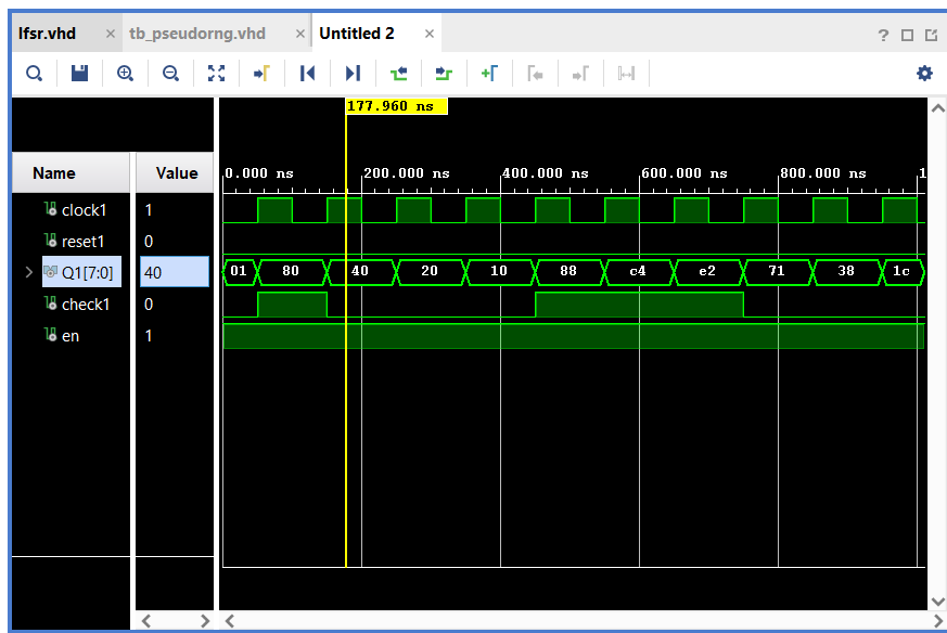
This LFSR can be modeled as a finite state machine (FSM) with a total number of states = 2^8 -1. As the all 0's state is of no use, we subtract 1.
This means an 8-bit LFSR will generate 255 distinct 8-bit random numbers, which one can use for applications in simple games or even for simple cryptographic applications. This is why it is also called a pseudo-random number generator, as the combinations here are limited to 255 and will repeat from a fixed set of 255 values. TRNGs or true random number generators are also possible but they cannot be modelled as FSMs, and they use physical parameters to generate random numbers such as thermal noise or radioactive decay.
In this blog, I showed some simple digital logic designs and advanced designs such as MUX and random number generator.
In the next blog, I will show how to control logic circuits by using hardware components such as switches and LEDs. I will talk about interfacing these components with the FPGA and experiment with them.
