


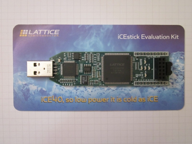
Introduction
A good while back, when I purchased an ADALM1000, I realised that Farnell had the Lattice
ICEstick back in stock so I bought one of those too. I thought it would be nice to do a simple
project, with a few of my impressions of the board thrown in along the way for good measure;
so a sort of informal review.
What is the iCEstick?
The iCEstick is an EVB (Evaluation Board) for one of Lattice's range of iCE FPGAs, namely the
iCE40HX1K. It has a device programmer on the board - so no need for a separate programmer -
and it can be plugged directly into a USB port: very convenient if you want to use it with a
laptop or a desktop PC to quickly try something, but maybe a little awkward once you get to
the stage of connecting prototype circuitry to it, though there's no reason it couldn't be run
on an extender cable. When these were first introduced, the price was very reasonable (~£20),
but now they're getting increasingly expensive. Farnell currently list them for £122.78
(ouch!).
The ICE40HX1K device on the board is a small FPGA by modern standards. The 1K stands for the
approximate number (actually 1280) of LEs (Logic Elements), where each LE contains both a
single 4-input look-up table, which can implement combinatorial logic, and a single D-type
flip-flop, which gives the memory element. The intended use would be logic replacement, or
fairly simple interfacing and control alongside a small processor. In terms of scale, it's
fine for learning the principles of how to design programmable logic, and how to develop with
either Verilog or VHDL, but will quickly run out of capability with more complex projects.
I'll be using VHDL, as that's what I know, but do note that the company that originally
developed these iCE parts (not Lattice) obviously worked with Verilog, as there often aren't
equivalent VHDL examples in the documentation and sometimes, where there are, they are
incomplete; so, if you're comfortable with Verilog, you would probably find it better to use
that with these parts. As well as the logic, there are sixteen 4K memory blocks - that's 4K
bits for each block - which can be arranged to have different widths (2,4,8,16 bits) and can
be used in a pseudo-dual-port mode (write one port, read the other); a single PLL for deriving
an internal clock from a clock input; and hard I2C and SPI interfaces (which I haven't tried
using), but note that one of the SPI is used for the initialisation. Much more limited than
what one of Lattice's more up-market device families would be capable of, but perfectly
adequate for many simple applications.
The HX series parts are faster than the LP devices - I assume HX stands for 'high speed' and
LP for 'low power'. Comparing speeds with FPGAs is always difficult, but in this case the
datasheet gives 160MHz for a simple 16-bit adder with the LP parts and 220MHz for the HX parts
(I think that might be an internal operating speed, rather than what you'd see if you attached
it to pins and measured the whole design, but I could be wrong), which suggests something like
a 30% - 40% gain with the HX devices. The speedup of the block RAM is more (twice as fast), so
the actual improvement in a real design could be very variable.
Of course, the big 'selling point' is there on the packaging: ice cold! By (older) FPGA
standards, they're low power.
iCEcube2
https://www.latticesemi.com/Products/DesignSoftwareAndIP/FPGAandLDS/iCEcube2
Lattice's proprietory software for designing with this part is called iCEcube2 and runs on
Windows (7 or 10 are the supported ones) or Linux (RHEL 6). Since I got the board, Lattice
have changed to charging, on a subscription model, for this design software. That didn't
matter to me, because I qualify to get it for free (maker/hobbyist/start-up), but it could
make developing with the parts quite expensive commercially if you don't qualify.
There is also an independent, open-source toolchain, too, which you might want to investigate,
but I'm going for the manufacturer's offering here.
I already had iCEcube2 installed (on Win 8.1), to use with another Lattice iCE device, so I
won't go through the installation. The Windows installer is only just over 700MB, so it's a
reasonably fast download and install.
The application has to be licensed. The licence lasts for one year and can either be tied to a
specific machine or floating (issued from a server) - I went for the simplicity of a fixed
licence. To get the licence, you'll need to set up a Lattice account. For the fixed licence,
you'll also have to give them the MAC address of the ethernet port on the machine as that's
what they're fixing the licence to: don't make the same mistake I did the first time when, not
really paying attention, I took the MAC of the WiFi from the ipconfig listing instead of the
one for the ethernet port.
The application is the usual kind of IDE that you get for developing FPGAs: edit windows on
tabs; an area for managing projects, files, and the design flow; and a panel for terminal
output messages. If you've used similar design software from other manufacturers, such as
Quartus from Altera (now Intel) or the old WebPack from the company once known as Xilinx (now
AMD), you won't have too much trouble adapting to this. However, be warned, this one is fairly
rudimentary. As the Lattice marketing department would have it: "Simple, Intuitive and Easy –
iCEcube2 offers a streamlined design flow for ease of use". Simple and easy, maybe, but I
might disagree slightly with the 'intuitive' claim.
For the synthesis, they offer a choice of their own LSE (Lattice Synthesis Engine) or
Synplify.
As is fairly common with FPGA manufacturers, Lattice don't have their own simulator and offer
a third-party one. In the past they've supplied one from Aldec, but now they've moved to
Mentor (now Siemens) ModelSim. The simulator is a 'Lattice edition', which I think means it
shares the licensing with the IDE and only has Lattice-specific libraries for the lower-level
post-synthesis simulation. It wasn't any trouble to install and get working, but I find the
hand-over between the IDE and the simulator messy and not very easy to understand from the
documentation.
A Simple Project
To try out the EVB I'm going to see if I can get it to produce some three-phase waveforms (so
three sine waves, each offset in phase by 120 degrees), at mains frequency (50Hz or 60Hz), by
look-up from block RAMS set up as ROMs (one for each phase), with delta-sigma DACs to do the
conversions (technically, I probably should call them 'modulators', as it only really becomes
a DAC once you integrate the output). The low-pass output filter is 3.2k, with 100nF to ground
(3.2k because I couldn't find any 3.3k SMD resistors and had to make it from a 1k in series
with a 2.2k).
I've rolled all the VHDL into one file. Here it is:
----------------------------------------------------------------------
--              ***** ice40hx1kevn_test.vhd *****                   --
--                                                                  --
-- ICE40HX1K evaluation board review test.                          --
-- Generates three-phase sine waves at either 50Hz or 60Hz          --
-- from look-up tables.                                             --
-- PLL takes 12MHz clock to 36MHz so that 50Hz and 60Hz can be      --
-- sample-accurate out of table for all three phases.               --
-- Simple delta-sigma DACs run from 36MHz clock.                    --
--                                                                  --
----------------------------------------------------------------------
-- (C)2025 Jon Clift                                                --
----------------------------------------------------------------------
-- Rev    Date         Comments                                     --
-- 01     14-June-2025                                              --
----------------------------------------------------------------------

library ieee;
use ieee.std_logic_1164.all;
use ieee.numeric_std.all;
use ieee.math_real.all;

entity ice40hx1kevn_test is port(
    clk_12:            in std_logic;          --- system clock in (from 12 MHz oscillator)
    select_50_60:      in std_logic;          --- freq select: 0=60Hz, 1=50Hz
    lock_out:          out std_logic;         --- PLL lock signal (test)
    sample_enable_out: out std_logic;         --- sample enable (test)
    clk_12_out:        out std_logic;         --- input clock out (test)
    clk_36_out:        out std_logic;         --- PLL output clock (test)
    dac_1_out:         out std_logic;         --- dac 1
    dac_2_out:         out std_logic;         --- dac 2
    dac_3_out:         out std_logic);        --- dac 3
end ice40hx1kevn_test;

architecture arch_ice40hx1kevn_test of ice40hx1kevn_test is

type MY_UNSIGNED_ARRAY_TYPE is array(255 downto 0) of UNSIGNED(15 downto 0);

signal sine_table1: MY_UNSIGNED_ARRAY_TYPE;
signal sine_table2: MY_UNSIGNED_ARRAY_TYPE;
signal sine_table3: MY_UNSIGNED_ARRAY_TYPE;
signal dac_1_data: UNSIGNED (15 downto 0);
signal dac_2_data: UNSIGNED (15 downto 0);
signal dac_3_data: UNSIGNED (15 downto 0);
signal sample_enable: STD_LOGIC;
signal clk_36: STD_LOGIC;
signal locked: STD_LOGIC;
signal locked_del: STD_LOGIC;
signal reset: STD_LOGIC;
signal pll_lock_out: STD_LOGIC;
signal sample_rate_prescale_count: UNSIGNED(11 downto 0);
signal sine_table_index: UNSIGNED(7 downto 0);

attribute FEEDBACK_PATH : string;
attribute FEEDBACK_PATH of pll_1 : label is "EXTERNAL";
attribute DELAY_ADJUSTMENT_MODE_FEEDBACK : string;
attribute DELAY_ADJUSTMENT_MODE_FEEDBACK of pll_1 : label is "FIXED";
attribute DELAY_ADJUSTMENT_MODE_RELATIVE : string;
attribute DELAY_ADJUSTMENT_MODE_RELATIVE of pll_1 : label is "FIXED";
attribute PLLOUT_SELECT : string;
attribute PLLOUT_SELECT of pll_1 : label is "GENCLK";

--- declare my sigma-delta modulator component

component delta_sigma_mod is
    generic(
        in_res: POSITIVE);           --- input resolution
    port (
        clk_in: in STD_LOGIC;
        data: in SIGNED(in_res-1 downto 0);
        mod_out: out STD_LOGIC);
end component;

--- declare Lattice PLL component

component SB_PLL40_CORE is
    generic (
        DIVR: integer;
        DIVF: integer;
        DIVQ: integer;
        FILTER_RANGE: integer;
        FEEDBACK_PATH: string;
        EXTERNAL_DIVIDE_FACTOR: integer;
        DELAY_ADJUSTMENT_MODE_FEEDBACK: string;
        FDA_FEEDBACK: integer;
        DELAY_ADJUSTMENT_MODE_RELATIVE: string;
        FDA_RELATIVE: integer;
        SHIFTREG_DIV_MODE: integer;
        PLLOUT_SELECT: string;
        ENABLE_ICEGATE: integer);
    port (
        REFERENCECLK: in STD_LOGIC;
        RESETB: in STD_LOGIC;
        BYPASS: in STD_LOGIC;
        EXTFEEDBACK: in STD_LOGIC;
        DYNAMICDELAY: in STD_LOGIC_VECTOR(7 downto 0);
        LATCHINPUTVALUE: in STD_LOGIC;
        SCLK: in STD_LOGIC;
        SDI: in STD_LOGIC;
        SDO: in STD_LOGIC;
        LOCK: out STD_LOGIC;
        PLLOUTGLOBAL: out STD_LOGIC;
        PLLOUTCORE: out STD_LOGIC
        );
end component;

begin

    --- Process to calculate three sine tables (one for each phase), instantly, at the start, and then wait forever
    --- Each table holds the 240 16-bit (signed) samples I need for the waveform
    --- Note that tables start at address 16 and not 0
    --- Don't use LSE to synthesize, use Synplify Pro: for some reason, LSE doesn't like the indefinite wait at the end,
    --- even though it works using LSE, in Diamond, targetting an XP2 part
    --- Although this is only (strictly speaking) meaningful for simulation, I'm hoping that
    --- the synthesis is clever enough to understand that it's equivalent to
    --- precalculating all of the sines and preloading them into BRAMs set up as a ROMs
    --- To help improve my chances, I've specified the size of the values to be 16-bit
    --- and padded the number of values, so that there's 256 of them, which then gives the basic size of a single block RAM
    --- for each table

    sine_table_calc_process: process
    begin
        sine_calc2: for i in 0 to 15 loop
            sine_table1(i) <= to_unsigned(0,16);    --- padding
            sine_table2(i) <= to_unsigned(0,16);    --- padding
            sine_table3(i) <= to_unsigned(0,16);    --- padding
        end loop sine_calc2;
        sine_calc1: for i in 16 to 255 loop
            sine_table1(i) <= to_unsigned(integer(round(((2.0**14.0 * sin((real(i-16)/240.0) * math_2_pi)) +  2.0**15.0))),16);
            sine_table2(i) <= to_unsigned(integer(round(((2.0**14.0 * sin(((real((i-16) + 160))/240.0) * math_2_pi)) +  2.0**15.0))),16);
            sine_table3(i) <= to_unsigned(integer(round(((2.0**14.0 * sin(((real((i-16) + 80))/240.0) * math_2_pi)) +  2.0**15.0))),16);
        end loop sine_calc1;
        wait;
    end process sine_table_calc_process;

    --- main process divides down 36MHz clock to give the sample rate, updates the table addresses at that rate, and pulls out
    --- values to send to the modulators.

    evb_test_stuff: process (clk_36) is
    begin

        if (clk_36'event and clk_36='1') then

            --- synchronous reset from rising edge of pll lock

            locked <= pll_lock_out;
            locked_del <= locked;
            reset <= locked and not locked_del;

            --- divide clock to get enable at the sample rate
            --- for 60Hz: 36MHz/2500 = 14.4ksps
            --- for 50Hz: 36MHz/3000 = 12ksps

            if (reset = '1') then
                sample_rate_prescale_count <= b"000000000001";
                sample_enable <= '0';
            elsif(sample_rate_prescale_count = b"000000000000") then
                if (select_50_60 = '1') then
                    sample_rate_prescale_count <= b"100111000100";   --- 2500
                else
                    sample_rate_prescale_count <= b"101110111000";   --- 3000
                end if;
                sample_enable <= '1';
            else
                sample_rate_prescale_count <= sample_rate_prescale_count - 1;	--- count down
                sample_enable <= '0';
            end if;

            --- table addressing

            if (reset = '1') then
                sine_table_index <= b"00010000";
            else
                if (sample_enable = '1') then
                    if(sine_table_index = b"11111111") then
                        sine_table_index <= b"00010000";
                    else
                        sine_table_index <= sine_table_index + 1;
                    end if;
                end if;
            end if;

            --- table look-up

            dac_1_data <= sine_table1(to_integer(sine_table_index));
            dac_2_data <= sine_table2(to_integer(sine_table_index));
            dac_3_data <= sine_table3(to_integer(sine_table_index));

        end if;

    end process evb_test_stuff;

    clk_36_out <= clk_36;
    clk_12_out <= clk_12;
    sample_enable_out <= sample_enable;
    lock_out <= pll_lock_out;

    --- instantiate and connect the Lattice SB_PLL40_CORE component
    --- (since there don't seem to be any examples for VHDL, I had to guess how to translate
    --- from the Verilog generated by the PLL tool - let's see if it works)
    --- this is for
    ---   12MHz in, 36MHz out
    ---   input from global clock (ie routing fabric)
    ---   feedback via routing fabric
    ---   no adjustment delays

    pll_1: component SB_PLL40_CORE
        generic map(
            DIVR => 0,
            DIVF => 47,
            DIVQ => 4,
---            DIVQ => 3,
            FILTER_RANGE => 1,
            FEEDBACK_PATH => "SIMPLE",
            EXTERNAL_DIVIDE_FACTOR => 0,
            DELAY_ADJUSTMENT_MODE_FEEDBACK => "FIXED",
            FDA_FEEDBACK => 0,
            DELAY_ADJUSTMENT_MODE_RELATIVE => "FIXED",
            FDA_RELATIVE => 0,
            SHIFTREG_DIV_MODE => 0,
            PLLOUT_SELECT => "GENCLK",
            ENABLE_ICEGATE => 0)
        port map(
            REFERENCECLK => clk_12,
            RESETB => '1',
            BYPASS => '0',
            EXTFEEDBACK => open,
            DYNAMICDELAY(7 downto 0) => b"00000000",
            LATCHINPUTVALUE => open,
            SCLK => open,
            SDI => open,
            SDO => open,
            LOCK => pll_lock_out,
            PLLOUTGLOBAL => clk_36,
            PLLOUTCORE => open
            );

    --- finally, instantiate and connect the three delta-sigma components

    dac_1: component delta_sigma_mod                    --- phase 1 output DAC
        generic map(
            in_res => 16)  --- resolution
        port map(
            clk_in => clk_36,
            data => dac_1_data (15 downto 0),
            mod_out => dac_1_out);

    dac_2: component delta_sigma_mod                    --- phase 2 output DAC
        generic map(
            in_res => 16)  --- resolution
        port map(
            clk_in => clk_36,
            data => dac_2_data (15 downto 0),
            mod_out => dac_2_out);

    dac_3: component delta_sigma_mod                    --- phase 3 output DAC
        generic map(
            in_res => 16)  --- resolution
        port map(
            clk_in => clk_36,
            data => dac_3_data (15 downto 0),
            mod_out => dac_3_out);

end arch_ice40hx1kevn_test;

--- Delta-Sigma Modulator component

library ieee;
use ieee.std_logic_1164.all;
use ieee.numeric_std.all;

entity delta_sigma_mod is
    generic(
        in_res: POSITIVE);                              --- input resolution
    port(
        clk_in: in STD_LOGIC;                           --- clock in
        data: in UNSIGNED(in_res-1 downto 0);             --- data in
        mod_out: out STD_LOGIC);                        --- output
end entity delta_sigma_mod;

architecture arch_delta_sigma_mod of delta_sigma_mod is

signal delta_add: SIGNED (in_res+1 downto 0);
signal sigma_add: SIGNED (in_res+1 downto 0);
signal sigma_latch: SIGNED (in_res+1 downto 0);
signal delta_in_a: SIGNED (in_res+1 downto 0);
signal delta_in_b: SIGNED (in_res+1 downto 0);

begin

    delta_in_a <= to_signed(to_integer(data),in_res+2);
    delta_in_b(in_res-1 downto 0) <= (others => '0');
    delta_in_b(in_res) <= sigma_latch(in_res+1);
    delta_in_b(in_res+1) <= sigma_latch(in_res+1);

    mod_clocked_stuff: process (clk_in)
    begin

        if (clk_in'event and clk_in='1') then
            sigma_latch <= sigma_add;
        end if;

    end process mod_clocked_stuff;

    delta_add <= delta_in_a + delta_in_b;
    sigma_add <= delta_add + sigma_latch;
    mod_out <= sigma_latch(in_res+1);

end arch_delta_sigma_mod;
Some Design Decisions I Made Along the Way
Rather than instantiate and initialise the ROMs, using the BRAM components that Lattice
provides, I decided to try and infer them in the code. As an experiment, rather than use the
case statement that they suggest to get inferred ROM content in place, I've had a go at
calculating the table values as an additional run-once-and-wait process - using the VHDL math
library. This may or may not work, we'll see.
I've chosen to have just two fixed output frequencies, 50Hz and 60Hz, selected by a switch on
a logic input. If I'm careful with the sample rate, so that the table entries correspond to
actual sample times, I'll be able to work with quite a small table yet retain the resolution
of the table entry (a 16-bit value). I went for 240 samples in a cycle as that almost fills a
single BRAM. The sample rate then needs to be 14.4ksps for 60Hz output and 12kps for 50Hz. I
can't derive both of those accurately from the 12MHz clock input, but if I multiply the 12MHz
by 3 with the PLL to give 36MHz, the subsequent divide values are 2500 for 60Hz and 3000 for
50Hz, which seem reasonable to work with. I'll also use the 36MHz for the sigma-delta stuff,
so the whole design is synchronous to the one 36MHz clock coming from the PLL - that should
save me from any timing problems, as it's comfortably within what the chip can manage. The
output files from the clock generator tool are in Verilog, so I've had a go at translating
them to VHDL, rather than work mixed-language - those files are only a wrapper for the Lattice
PLL 'black box', so it should work exactly the same. I decided it was worth a quick experiment
to see.
For the logic working at the sample rate, I've used a clock qualifier (sample_enable) to the
36MHz clock rather than messing around with a separate, slower clock. That's a very safe way
to design - there can't be any difficulties handing over between clock domains if there's only
one clock - and it's a way that the FPGA designers expect you might adopt because there are
always clock enables on clocked components and the design software will usually recognise what
you're doing and place the qualifier signal on fast global routing (but, obviously, check
anyway).
The VHDL component for the delta-sigma converter I based on information in a Xilinx app note,
never having done one before. It seems to work, but don't trust any of this without further
examination - I'm just slapping it together, without even simulating, so no guarantees
whatsoever.
Synthesis
LSE wouldn't synthesize it because it objected to the wait (at the end of the calculation
process) not having a parameter.
That's odd, because previously I've done the same thing with LSE targetting an XP2 device in
Diamond, and there LSE quite happily accepted the indefinite wait.
Luckily for me, Symplify was ok with it and also seems to have taken the heavy hint that I
want three look-up tables (the 3 tables all appear instantiated in the timing simulation VHDL
file, along with plausible-looking initialisation statements).
Place and Route
I'm going to bring out all the top-level entity port pins, except for the clock, to the PMOD
connector on the board. Here's the relevant part of the schematic from the user guide.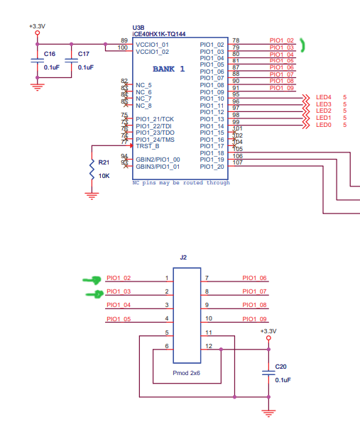
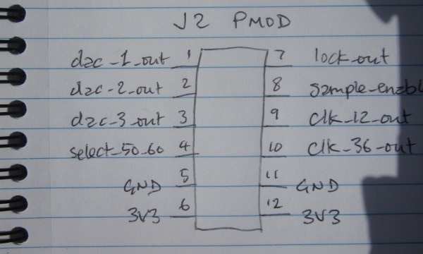
If I choose pins 1, 2, and 3 on the PMOD connector (J2), I can see that they connect to pins
78, 79, and 80 on the FPGA itself. It's those FPGA pin numbers that I'll need for the
constraints for the place and route. If I don't constrain the outputs to be particular pin
numbers, the design software will just allocate the pins for itself as it thinks best. I'll
also need a constraint for the clock input, to make sure that it comes from the existing on-
board xtal oscillator (12MHz, shared with the FTDI USB chip) on pin 21.
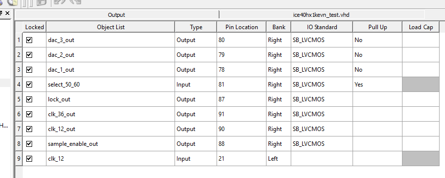
To do this, there's a simple pin editor, on the tool bar, that presents a table of the pins
found in the design and allows the pin numbers to be set. Each pin can be locked if desired.
That leads to this arrangement on the connector itself, viewed from the top. Pin one can be identified by the square pad on the underside of the board. Be cautious of the silkscreen on the top - none of it relates to the PMOD, it's all labelling for the rows of pins along the two board edges.
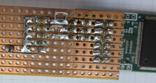
And, here's the board that I implemented the output filters on. Be aware that the dac outputs may radiate nicely given the chance. When I first tested, without the filter, it wiped out an FM radio a couple of metres away when a scope probe was used to look at one of the outputs. Presumably the signal was driving the outside of the probe cable screen.
The place-and-route ran fine, and generated several bitmaps. There's more than one as you get
binary, a couple of hex formats, and something else, to facilitate the different ways the
bitstream can get into the FPGA: maybe from an SPI memory chip, maybe from a processor, or
maybe injected directly into the internal configuration SRAM of the FPGA by the programmer.
Now I have to program the board. Somewhat awkwardly, that's done from another piece of
software that isn't integrated into the IDE - the Diamond programmer working stand-alone. I'd
strongly suggest that, the first time you do this, you follow the steps in the ICEstick user
guide - I'm familiar with using the programmer, from within Diamond, but I'd have got in a
muddle if I had tried to guess what to do with the iCEstick. If you save the programming
setup, subsequent programming is then as easy as loading the setup (it presents you with the
last used) and clicking the program button on the tool bar, which can all be done within a few
seconds. One thing to be aware of is that the configuration memory on my iCEstick was
different to the one given in the documentation, so you'll need to adapt the setup of the
programming to take that into account.
Results
To start with: is the PLL working OK? I've brought both clocks out to pins on the PMOD
connector so that I can look at them on an oscilloscope. Here, the bottom trace is the 12MHz xtal
osc clock passed through the FPGA and the top trace is the 36MHz clock produced by the PLL.
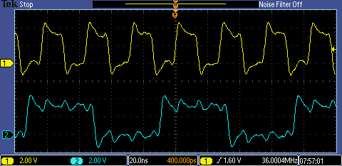
Ignoring the ringing - sloppy probing - it has managed to multiply the 12MHz by three, so my
VHDL for the PLL must be roughly right. I'm using the simple, internal feedback in the PLL, so
there's no attempt to align the two by feeding back from the fabric (no need with this).
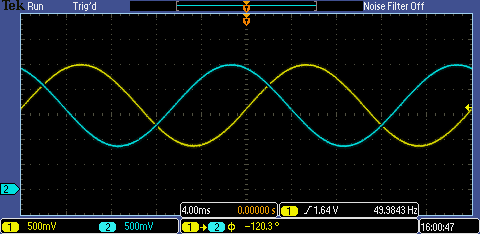
Now that I know I've got a working clock, we can move to the sinewaves, 50Hz first. I only
have a 2-channel oscilloscope, so the first trace shows 1 and 2 and the second trace shows 1
and 3 (yellow is output one in each case).
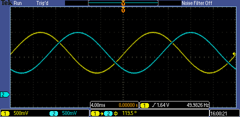
Here's the last one again, with the frequency switched to 60Hz.

Conclusions
The FPGA
- simple, basic, fairly cheap, and with easy-to-work-with device packages: just right for a
lot of small projects.
- does have limitations, which you'll feel if you've gotten used to more capable devices
- apparently, though I didn't investigate very far, all the F/Fs initialise to zero, so you
either need to work with that, or find a way of implementing your own reset
- a chip errata says that the first table value doesn't get loaded from the bitstream, which
is why I put the padding at the start of the table
- probably works best if you have a reasonable amount of knowledge and experience of actual
logic design and can target a design tightly to the capabilities of the device
The EVB
- convenient having the programmer on-board
- no frills: just FPGA, programmer, config memory, and clock osc
- I don't think anyone, anywhere, would now say it's 'value for money'
- very limited on the IO side. The 144 pin QFP part has lots of pins - very few of them make
it to the connectors
Design software
- simple, lightweight, and fast
- not always very intuitive
- choice of synthesis (LSE or Symplify), which helped me here
- simulator 'integration' isn't wonderful
Alternatives
There seem to be quite few small iCE boards now. Perhaps some of that is stemming from the
availability of an open toolchain.
One example is this much more affordable alternative to the iCEstick from Olimex.
https://www.olimex.com/Products/FPGA/iCE40/iCE40HX1K-EVB/open-source-hardware
It doesn't have a programmer on the board, though. They seem to work on the basis you'll use
the open-source toolchain and rig up a small SBC to program it via SPI (which, to be fair,
shouldn't be too difficult). They do, however, throw in an additional 512KB SRAM, which might
well be of interest.
That board is also available loaded with a much more generous 8K iCE40 HX part.
Further information
[1] https://uk.farnell.com/lattice-semiconductor/ice40hx1k-stick-evn/ice40-hx1k-icestick- eval-kit/dp/2355207
[2] https://www.latticesemi.com/products/developmentboardsandkits/icestick
[3] DS588 XPS Delta-Sigma Digital to Analog Converter (DAC). Xilinx 2009.


