


The idea of this little manual is to help FPGA beginners. Like everyone in the world we are not born knowing, and it is always useful to help so that the beginnings are not so difficult.
I assume that if you are going to enter in the FPGA world, you will have already installed and tested the program with which you are going to develop the project. For this reason I will skip the steps of creating a project and adding the different evaluation boards to the programs. In this case I am going to develop the manual in VHDL and VIVADO, and then implement it in CMODS7. Anyway, I leave you the following links to official Digilent tutorials, in which he explains the aforementioned.
Installing Vivado and board files: https://reference.digilentinc.com/vivado/installing-vivado/start
Starting with Vivado: https://reference.digilentinc.com/vivado/getting_started/start
Next I leave the links of the CMODS7 board so that you can see the characteristics.
Schematics: https://s3-us-west-2.amazonaws.com/digilent/resources/programmable-logic/cmod-s7/Cmod+S7_sch-public.pdf
With all of the above we can already start designing our code. As an example I am going to make a communication by UART through the FTDI chip with the PC, and later we will control the 4 LEDs with commands.
1. Clock Generation
The first step is to create a global clock. The oscillator of the CMODS7 is 12 Mhz, enough for the manual, but we are going to use a mixed-mode clock manager (MMCM) to generate a 100 MHz clock (for learning purposes). To do this, we select the CLOCK WIZARD in the Vivado IP catalog, and it will open a window that shows us the IP.
As we can see in the block on the left, it has 4 pins.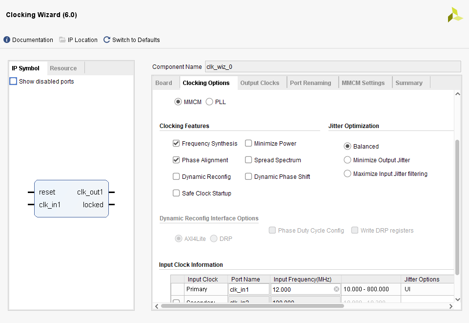
- reset: Reset signal to to initialize the module.
- clk_in1: Oscillator input signal.
- clk_out1: Clock signal that we use in the code.
- locked: Signaling signal that the frequency synthesizer is correctly set to the desired frequency.
To the right of the image we see that MMCM is marked, we leave the characteristics of the clock as they are and the only thing that needs to be modified is the value of clk_in, in this case 12MHz.
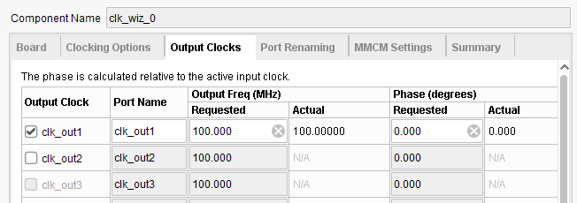
In the next step, we will modify the global clock to 100 MHz.
With this, we already have the clock IP configured, now we will only accept and mark the option OUT of context per IP. Now it only remains to define the block and make the instance in our TOP file.
COMPONENT clk_wiz_0
        PORT(       clk_in1         : IN STD_LOGIC;
                    clk_out1        : OUT STD_LOGIC ;
                    reset           : IN STD_LOGIC;
                    locked          : OUT STD_LOGIC );
END COMPONENT;
new_clock   :   clk_wiz_0 PORT MAP (    clk_in1       => clk_pin,
                                         clk_out1      => clk,
                                         reset         => '0',
                                         locked        => open);
In this case, I am not going to use the reset and locked signals, so the reset signal in low level and the locked signal unconnected.
2. UART code
To make the communication between the PC and the FPGA, we use a UART code developed by Scott Larson for Digi-key. On the next page we have enough sample codes that can be used for your projects.
Example VHDL codes: https://www.digikey.com/eewiki/display/LOGIC/Home
The UART code works fine, but I have found a small bug and I have already contacted them with the solution. For now he has not corrected it yet. At the end of the tutorial I will share the entire project, so the modification will be made to solve this bug.
In this code we can configure the UART parameters such as baud rate, parity bit, etc.
GENERIC(
        clk_freq      :    INTEGER        := 100_000_000;    --frequency of system clock in Hertz
        baud_rate     :    INTEGER        := 9_600;          --data link baud rate in bits/second
        os_rate       :    INTEGER        := 16;             --oversampling rate to find center of receive bits (in samples per baud period)
        d_width       :    INTEGER        := 8;              --data bus width
        parity        :    INTEGER        := 0;              --0 for no parity, 1 for parity
        parity_eo     :    STD_LOGIC      := '0');           --'0' for even, '1' for odd parity
In our case we have to configure clk_fre, which is the frequency of the 100 MHz global clock and the baud rate that we are going to use 9600 bps. The rest we will not modify, since by default it is correct.
Basically the code is two state machines, one for each line (receive and transmit) and a pulse generator for the baud rate. Anyway, all the code is explained very well on the next page.
UART code: https://www.digikey.com/eewiki/pages/viewpage.action?pageId=59507062
Again, we have to define the block and instantiate it in the TOP file.
COMPONENT uart_MCU
        PORT(       clk         :    IN STD_LOGIC;                                      --system clock
                    reset_n     :    IN STD_LOGIC;                                      --ascynchronous reset
                    tx_ena      :    IN STD_LOGIC;                                      --initiate transmission
                    tx_data     :    IN STD_LOGIC_VECTOR(7 DOWNTO 0);                   --data to transmit
                    rx          :    IN STD_LOGIC;                                      --receive pin
                    rx_busy     :    OUT STD_LOGIC;                                     --data reception in progress
                    rx_error    :    OUT STD_LOGIC;                                     --start, parity, or stop bit error detected
                    rx_data     :    OUT STD_LOGIC_VECTOR(7 DOWNTO 0);                  --data received
                    tx_busy     :    OUT STD_LOGIC;                                     --transmission in progress
                    tx          :    OUT STD_LOGIC);                                    --transmit pin
END COMPONENT;
MCU_uart    :   uart_MCU PORT MAP (         clk         => clk,
                                            reset_n     => mr,
                                            tx_ena      => tx_eM,
                                            tx_data     => tx_dM,
                                            rx          => sRX_MCU,
                                            rx_busy     => rx_bM,
                                            rx_error    => rx_PM,
                                            rx_data     => rx_dM,
                                            tx_busy     => tx_bM,
                                            tx          => sTX_MCU);
3. Data control
The next thing we need is a controller to send and receive the data through the UART. This code will take the data received from the UART, filter it to eliminate unwanted characters, control the LEDs and send a string of characters to the PC.
The LEDs will change state with the Lx command (where x is 1,2,3 and 4), if x is different from these values then the LEDs will turn off.
First of all, we need to know when the UART block has received complete data. For this I have taken the RX busy signal as a reference, when this signal is '1' it is receiving data. Whereas if it is '0' the data has already been received or there is no data. Therefore, when the falling edge occurs in RX busy, the received data will be ready to process it. What I have done has been to delay the Rx busy signal and make an AND with itself to invert it. With this we will create a clock cycle pulse when the falling edge of the Rx busy signal occurs.
PROCESS(clk)
        BEGIN
            IF (mr = '1') THEN
                r_busy_0 <= '0';
                r_busy_1 <= '0';
            ELSIF (clk = '1' AND clk'event) THEN
                r_busy_0 <= Rx_busy;
                r_busy_1 <= r_busy_0;
            END IF;
   END PROCESS;

   new_data <= (NOT(r_busy_0) AND r_busy_1);
Now, we just have to take the "L" character (0x4C in HEX). We have to check if a new data has been received and if it is equal to 0x4C. If this is the case, we can continue and check if another character has arrived after the 0x4C character.
PROCESS (clk)
    BEGIN
        IF (mr='1') THEN
            CABECERA <= '0';
            CABE_DATA <= (others => '0');
        ELSIF(clk = '1' AND clk'event) THEN
            IF (new_data = '1' AND CABECERA = '0' AND Rx_data = X"4C") THEN
                CABE_DATA <= Rx_data;
                CABECERA <= '1';
            ELSIF (FIN = '1') THEN
               CABECERA <= '0';
               CABE_DATA <= (others => '0');
            END IF;
        END IF;
    END PROCESS;

    new_data_cab <= NOT(r_busy_0) AND r_busy_1 AND CABECERA;
Finally, once the next character is received (only if it is 1 - 4) the selected led will change state. As I mentioned previously, implement a small code that sends a confirmation frame to the PC that the Led has been modified. This frame is ("\ n \ r OK \ n \ r").
PROCESS (clk)
    VARIABLE CNT    : INTEGER range 0 to 6;
    BEGIN
        IF (mr='1') THEN
            CNT := 0;
            sig <= '0';
            FIN <= '0';
            LED1 <= '0';
            LED2 <= '0';
            LED3 <= '0';
            LED4 <= '0';
            Tx_01 <= '0';
            Tx_data <= (others => '0');
        ELSIF(clk = '1' AND clk'event) THEN
        IF (CABECERA = '1' AND CABE_DATA = X"4C") THEN
             IF (new_data_cab = '1') THEN
                CASE Rx_data  IS
                    WHEN X"31"=> LED1 <= NOT(LED1);
                    WHEN X"32"=> LED2 <= NOT(LED2);
                    WHEN X"33"=> LED3 <= NOT(LED3);
                    WHEN X"34"=> LED4 <= NOT(LED4);
                    WHEN OTHERS => LED1 <= '0';
                                   LED2 <= '0';
                                   LED3 <= '0';
                                   LED4 <= '0';
               END CASE;
               sig <= '1';
            ELSIF (CNT = 6 AND Tx_busy = '1') THEN
                CNT := 0;
                FIN <= '1';
                sig <= '0';
                Tx_01 <= '0';
                Tx_data <= (others => '0');
            ELSIF (Tx_01 = '1' AND Tx_busy = '1') THEN
                Tx_01 <= '0';
            ELSIF ( Tx_busy = '0' AND sig = '1' AND Tx_01 = '0') THEN
                CASE CNT IS
                    WHEN 0 => Tx_data <= X"0A";
                    WHEN 1 => Tx_data <= X"0D";
                    WHEN 2 => Tx_data <= X"4F";
                    WHEN 3 => Tx_data <= X"4B";
                    WHEN 4 => Tx_data <= X"0A";
                    WHEN 5 => Tx_data <= X"0D";
                   When others => Tx_data <= X"00";
                END CASE;
                Tx_01 <= '1';
                CNT := CNT + 1;

            ELSE
                FIN <= '0';
            END IF;
        END IF;
       END IF;
    END PROCESS;
To finish the project, we need to perform the constraint. In this file each signal of the code will be designated with the pinout of the board.
# 12 MHz System Clock
set_property -dict {PACKAGE_PIN M9 IOSTANDARD LVCMOS33} [get_ports clk_pin]

# Push Buttons, reset
set_property -dict {PACKAGE_PIN D2 IOSTANDARD LVCMOS33} [get_ports simr]

# 4 LEDs
set_property -dict {PACKAGE_PIN E2 IOSTANDARD LVCMOS33} [get_ports Led1]
set_property -dict {PACKAGE_PIN K1 IOSTANDARD LVCMOS33} [get_ports Led2]
set_property -dict {PACKAGE_PIN J1 IOSTANDARD LVCMOS33} [get_ports Led3]
set_property -dict {PACKAGE_PIN E1 IOSTANDARD LVCMOS33} [get_ports Led4]

## USB UART
set_property -dict { PACKAGE_PIN L12   IOSTANDARD LVCMOS33 } [get_ports  sTX_MCU ];
set_property -dict { PACKAGE_PIN K15   IOSTANDARD LVCMOS33 } [get_ports  sRX_MCU ];
Having everything configured, we can carry out the synthesis of the project and obtain the schematic.
4. Test bench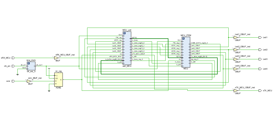
One of the biggest problems beginners have is performing test bench, they are often more tedious to write than the code itself. To help you I am going to share a page that will avoid the arduous task of repeating the writing process. All you have to do next is add the signals you need and the behavior.
Test bench online: https://vhdl.lapinoo.net/testbench/
In this case, I have used a function that sends a byte at the baud rate of 9600. Where c_BIT_PERIOD is 1/9600 = 104166 ns.
constant c_BIT_PERIOD : time := 104166 ns;

procedure UART_WRITE_BYTE (
    i_data_in       : in  std_logic_vector(7 downto 0);
    signal o_serial : out std_logic) is
  begin

    -- Send Start Bit
    o_serial <= '0';
    wait for c_BIT_PERIOD;

    -- Send Data Byte
    for ii in 0 to 7 loop
      o_serial <= i_data_in(ii);
      wait for c_BIT_PERIOD;
    end loop;  -- ii

    -- Send Stop Bit
    o_serial <= '1';
    wait for c_BIT_PERIOD;
end UART_WRITE_BYTE;
And the code to test the project, send the character L (0x4C) and 1 (0x31):
constant sms : std_logic_vector (15 DOWNTO 0) := X"4C31";

stimuli : process
    begin
        -- EDIT Adapt initialization as needed
        sRX_MCU <= '1';
        simr <= '0';

        -- Reset generation
        simr <= '1';
        wait for 100 ns;
        simr <= '0';
        wait for 100 ns;

 UART_WRITE_BYTE(sms(15 DOWNTO 8),sTX_MCU);
 UART_WRITE_BYTE(sms(7 DOWNTO 0),sTX_MCU);
        -- EDIT Add stimuli here
        wait for 10000 * TbPeriod;

        -- Stop the clock and hence terminate the simulation
        TbSimEnded <= '1';
        wait;
    end process;
We simulate it and see that the data is received correctly, Led1 lights up and the characters string is sent to the PC. The last data "\ r" (0x0D) does not appear in the transmission line, but it is because the change is very fast.
If we zoom in, we can see that it is indeed being sent.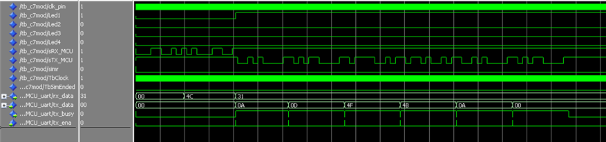
5. Test in CMODS7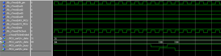
Time to program our CMODS7 and see if the code actually works.
6. Conclusion
As we can see, there are many open VHDL codes on the internet with which we can do interesting things. Also, I always recommend searching first before you head into programming, you can save a lot of time and headaches. On the other hand, I strongly recommend always doing the test benches, sometimes it is heavy to do but avoid many problems.
To finish I want to give a small assessment of CMODS7. For me, it is a very good board to start in the FPGA world, containing an FTDI makes it very manageable (as we have already seen, it is very easy to transfer and receive data from a PC). Another strong point is that of its small size and pins, it is very comfortable to perform the tests and integrate it into a breadboard with more electronics. I recommend it for small and medium projects, it is a good acquisition.